Article

Transient THz Emission and Effective Mass Determination in Highly Resistive GaAs Crystals Excited by Femtosecond Optical Pulses

1
Materials Science Graduate Program, University of Rochester, Rochester, NY 14627, USA
2
Laboratory for Laser Energetics, University of Rochester, Rochester, NY 14623, USA
3
Research Centre Jülich, Ernst Ruska Centre for Microscopy and Spectroscopy with Electrons, D-52425 Jülich, Germany
4
Department of Electrical and Computer Engineering, University of Rochester, Rochester, NY 14627, USA
5
Research Centre Jülich, Peter Grünberg Institute (PGI-6), D-52425 Jülich, Germany
6
Department of Physics, University of California Davis, Davis, CA 95616, USA
*
Author to whom correspondence should be addressed.
Crystals 2022, 12(11), 1635; https://doi.org/10.3390/cryst12111635
Submission received: 24 October 2022 / Revised: 7 November 2022 / Accepted: 11 November 2022 / Published: 14 November 2022

Abstract

:
We present comprehensive studies on the emission of broadband, free-space THz transients from several highly resistive GaAs samples excited by femtosecond optical pulses. Our test samples are characterized by different degrees of disorder, ranging from nitrogen-implanted to semi-insulating and annealed semi-insulating GaAs crystals. In our samples, we clearly observed transient THz emissions due to the optical rectification effect, as well as due to the presence of the surface depletion electrical field. Next, we arranged our experimental setup in such way that we could observe directly how the amplitude of surface-emitted THz optical pulses is affected by an applied, in-plane magnetic field. We ascribe this effect to the Lorentz force that additionally accelerates optically excited carriers. The magnetic-field factor η is a linear function of the applied magnetic field and is the largest for an annealed GaAs sample, while it is the lowest for an N-implanted GaAs annealed at the lowest (300 °C) temperature. The latter is directly related to the longest and shortest trapping times, respectively, measured using a femtosecond optical pump-probe spectroscopy technique. The linear dependence of the factor η on the trapping time enabled us to establish that, for all samples, regardless of their crystalline structure, the electron effective mass was equal to 0.059 of the electron mass m0, i.e., it was only about 6% smaller than the generally accepted 0.063m0 value for GaAs with a perfect crystalline structure.

1. Introduction

Generating broadband, free-space terahertz (THz) transients by pumping nonlinear semiconductor materials, such as, e.g., GaAs, with femtosecond optical laser pulses, is a well-established technique, generally called transient THz emission [1,2,3]. Several radiation models have been proposed to explain the THz emission; for example, surface depletion created by the internal electric field perpendicular to the sample surface [4,5,6,7], nonlinear optical rectification [8,9], and photocurrent generated by the photo-Dember effect [10,11,12]. These mechanisms, responsible for transient THz wave emission, usually coexist and are related [13]. The latter reveals the complexity of the THz-emitter efficiency optimization. The intensity and operation bandwidth of the transient THz emission are the most crucial parameters from the application perspective. The emission bandwidth is governed by the charge-carrier lifetime, which can be controlled by ion implantation [14] or, alternatively, via an embedded plasmonic metasurface [15]. It has been also demonstrated that an external magnetic field applied in the plane of a semiconductor can tune the amplitude of the surface-emitted THz radiation [16,17]. The enhancement of the THz amplitude is ascribed to the Lorentz force induced by the applied magnetic field, which introduces an additional acceleration to photocarriers [16,17]. The charge-carrier lifetime and mobility are the key parameters affecting the amount of the Lorentz-force-induced acceleration of photoelectrons. Femtosecond optical pump-probe spectroscopy is a technique [18] that can measure relaxation dynamics of nonequilibrium carriers and lifetime with the sub-picosecond time resolution. The results can establish, in a given semiconductor, the relationship between the transient THz signal and the carrier relaxation lifetime. A better understanding of this relationship should help us build an optimized THz emitter, with a signal that is enhanced by the magnetic field, using permanent, commercial magnets [19] and, ultimately, open up new possibilities for controlling the spectral composition, pulse shape, and energy of transient THz emissions [20].

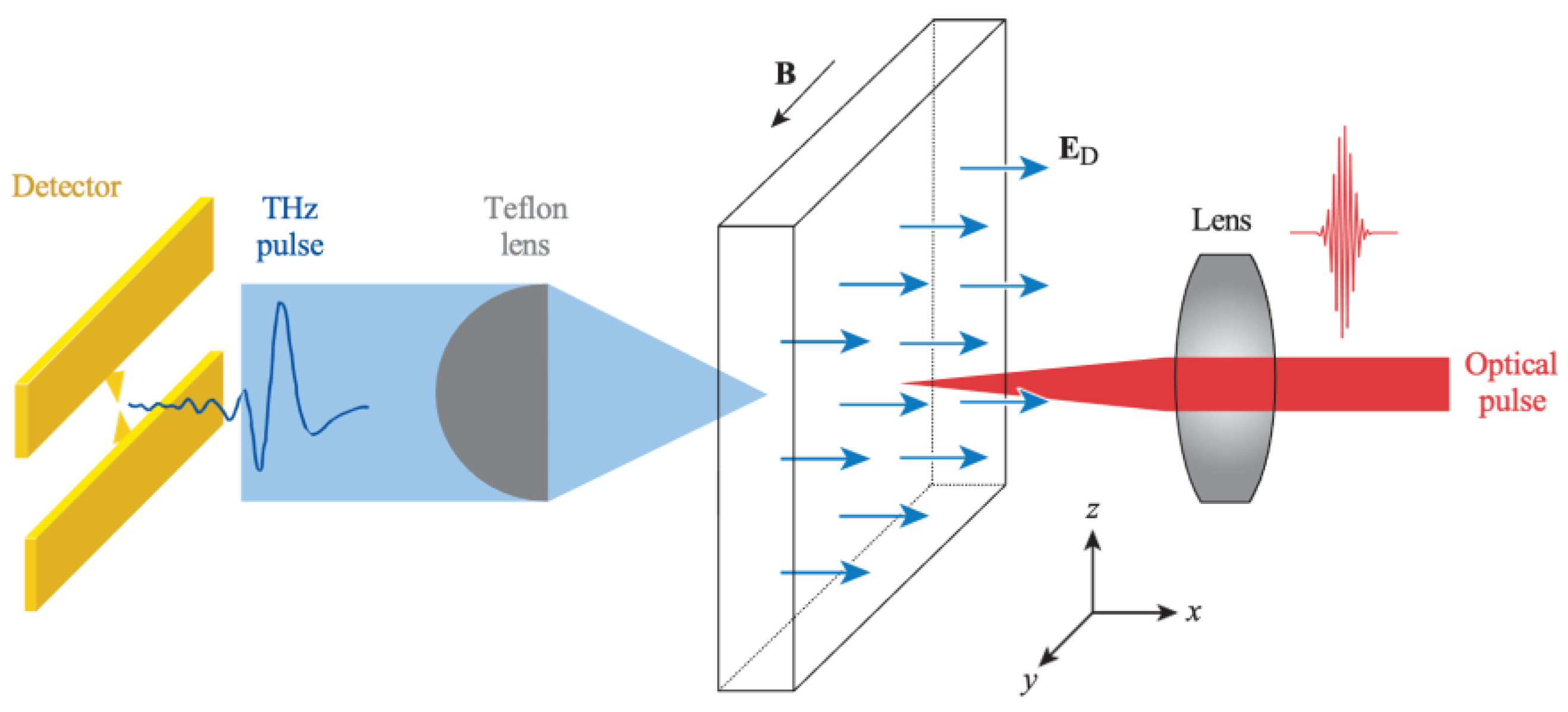
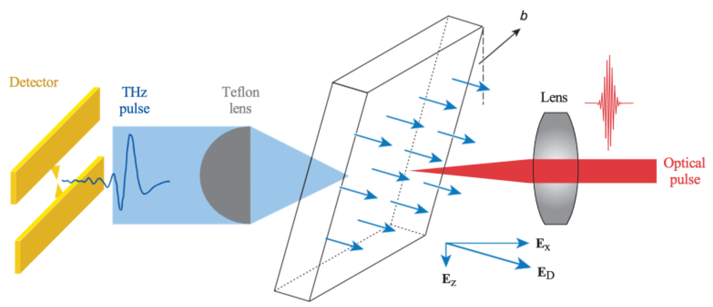
2. Materials and Methods

For our studies, we chose 5 different, highly resistive GaAs samples characterized by different mobilities and crystalline conditions, namely, a standard, Cr-doped, semi-insulating GaAs wafer (SI GaAs), the same semi-insulating GaAs sample, but annealed at 300 °C (Annealed GaAs), and three nitrogen-ion implanted GaAs specimens, implanted at an energy of 191 keV with a dose of ~8 × 10¹¹ ions/cm2 [21,22], and, subsequently, annealed at 300 °C, 350 °C and 400 °C, denoted as N-GaAs 300, N-GaAs 350, and N-GaAs 400, respectively. Since N-GaAs 300, N-GaAs 350, and N-GaAs 400 samples were, ultimately, intended for THz-band photomixers, their size was only 3 × 3 mm.2
Experiments were performed using THz time-domain spectroscopy (THz-TDS) and optical femtosecond pump-probe spectroscopy (F-PPS) systems. In both cases, we used a commercial Ti:Sapphire laser that generated a train of nominal, 100-fs-wide laser pulses at 800 nm wavelength and 76 MHz repetition rate. A Faraday isolator was aligned in front of the laser to avoid any light reflection back into the laser cavity. In our THz-TDS setup [23], the laser beam is split into two branches with a 90:10 power ratio. The high-power branch, after bouncing from a retroreflector mounted on a delay stage, is focused on our test GaAs sample to generate bursts of electromagnetic radiation, i.e., single-picosecond transients, with the frequency spectrum extending into THz, while the low-power laser beam is used for the THz transient detection and focused on a commercial low-temperature grown GaAs (LT-GaAs) photoconductive (PC) THz detector with z-axis polarization sensitivity (perpendicular to the optical table) [24]. A Teflon (polytetrafluoroethylene) lens with a 5 mm diameter and ~10 mm focal length, located between the test sample and the THz detector, collimates the transmitted THz radiation. In addition, an external magnetic field B is applied in the sample plane along the y-axis, while the emitted THz radiation is collected along the x direction, as indicated in Figure 1.
The F-PPS system was implemented to measure the nonequilibrium carrier dynamics in our samples. In this setup [25,26], optical pulses are split into two beams by a 60/40-beam splitter. Pump pulses have higher power, and the beam is modulated with an acousto-optic modulator. The lower-power probe beam is delayed with respect to the pump by reflection from a retroreflector mounted on a delay stage. Both pump and probe beams are focused on the same spot in the sample, the beam size of the probe (~20 μm in diameter) is kept slightly smaller than that of the pump beam (~30 μm in diameter) to make sure we only probe the optically excited area of the sample. To limit the probe-related electron heating to a minimum and ensure a decent signal-to-noise ratio, the probe beam is additionally attenuated using neutral density filters to set about a 10:1 power ratio between the pump and probe beams. The probe beam is reflected at the sample surface and directed toward a photodetector connected to a lock-in amplifier to record the normalized reflectivity change (ΔR/R) waveforms as a function of the time delay between the pump and probe pulses.

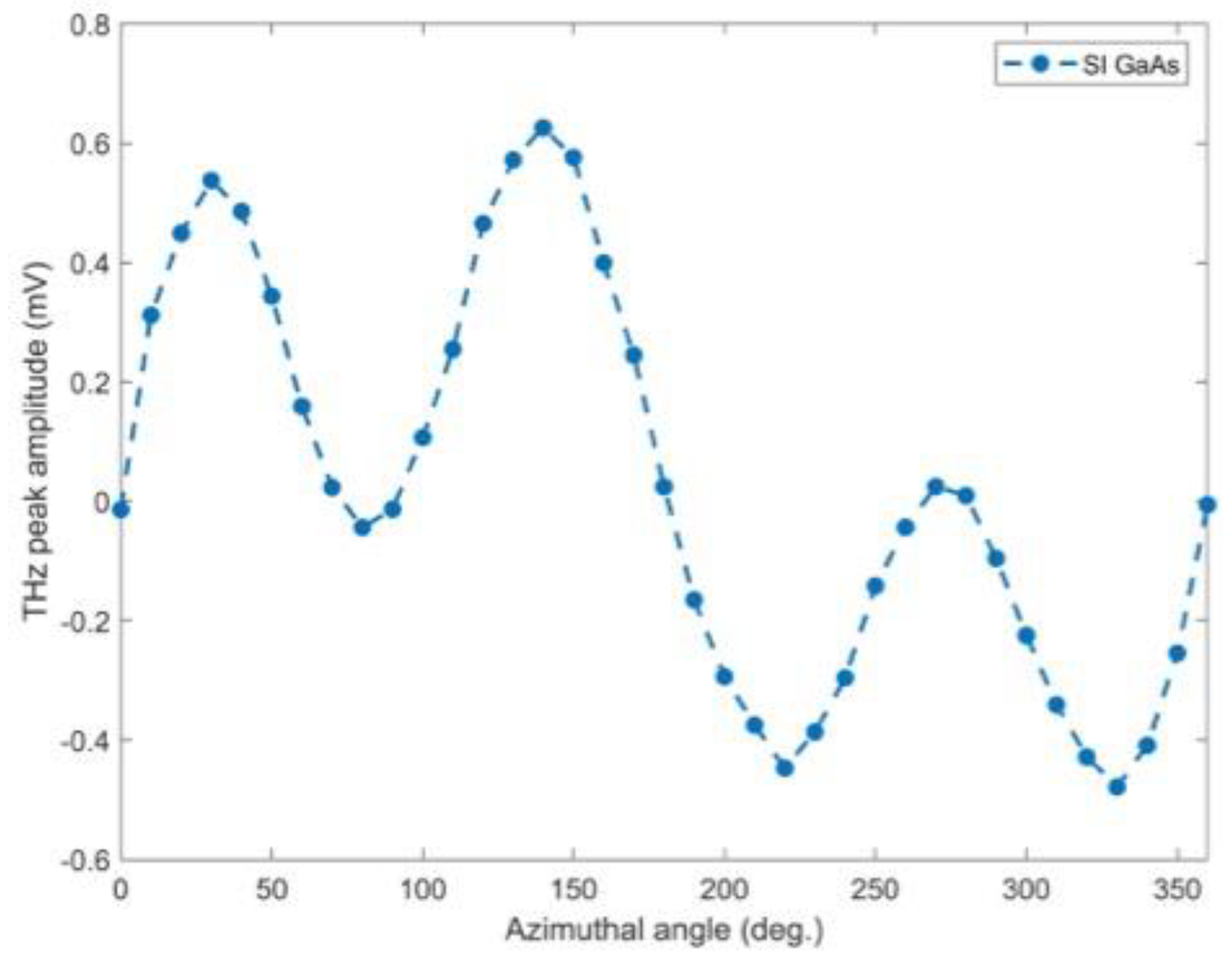
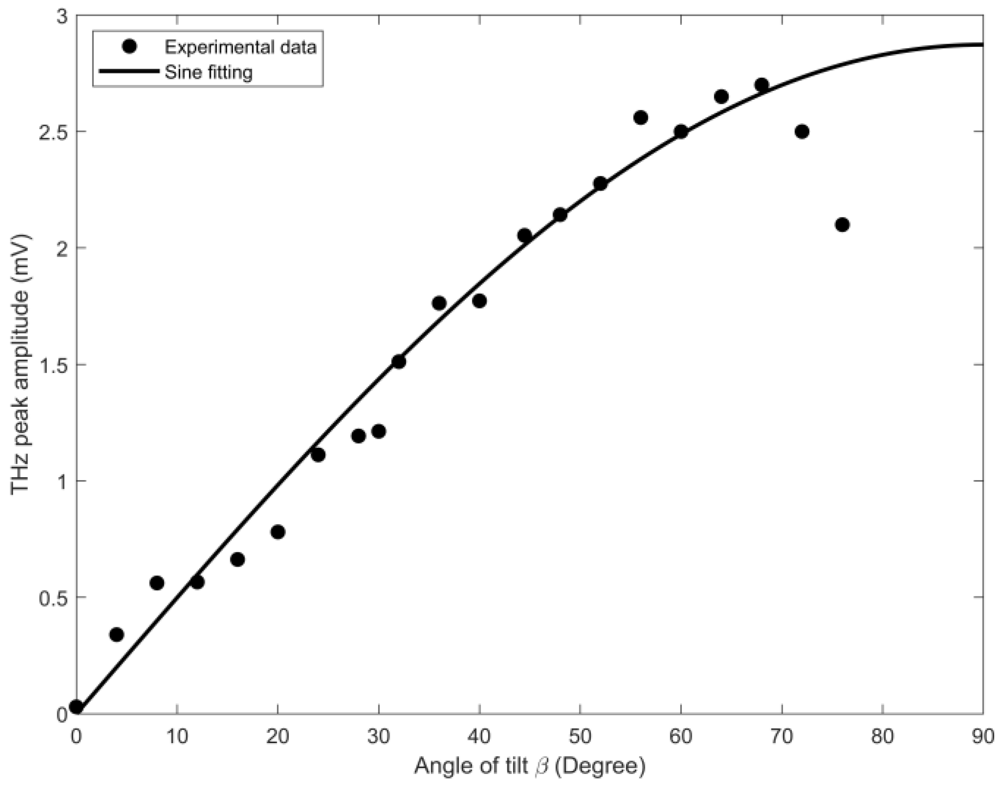
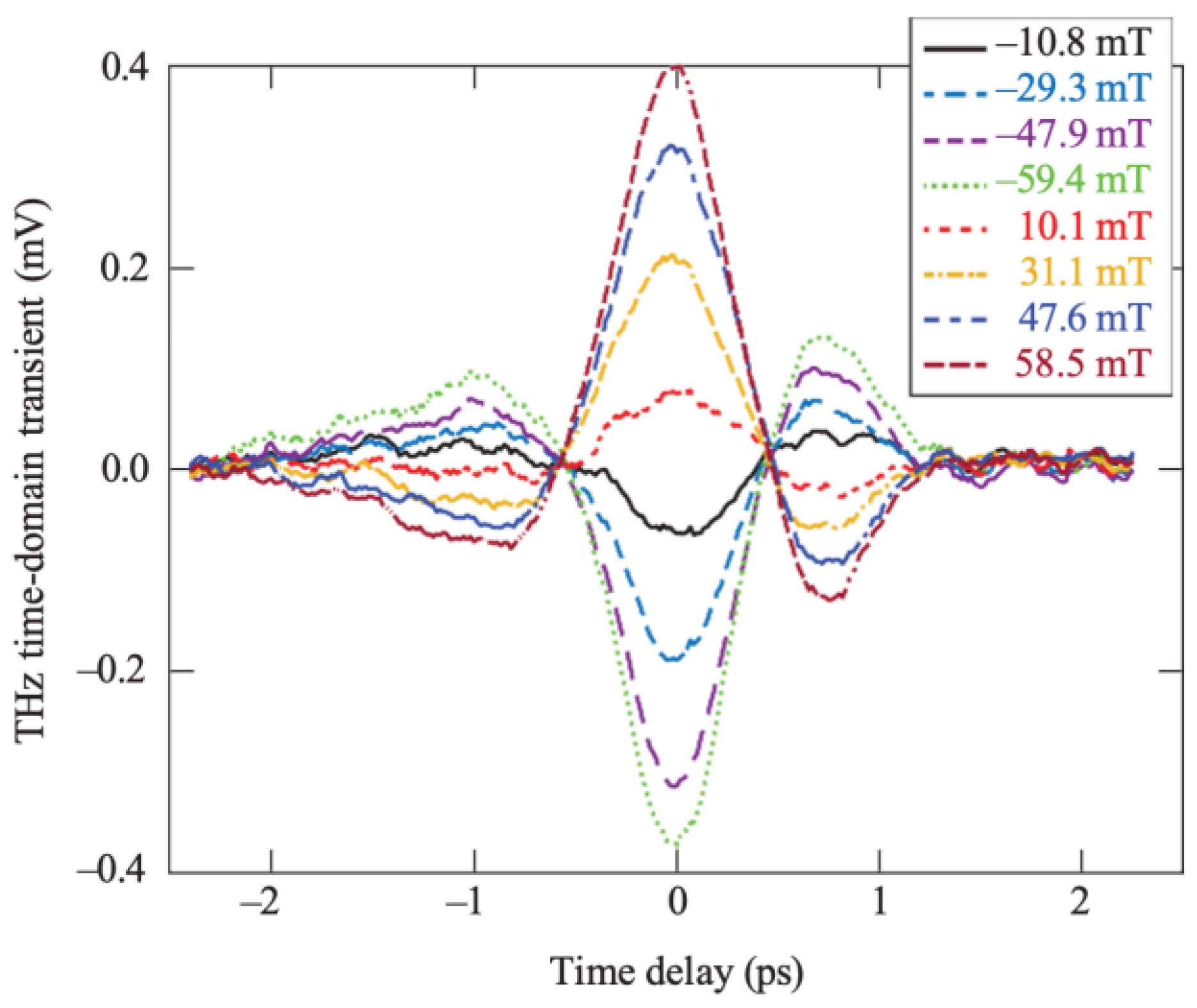
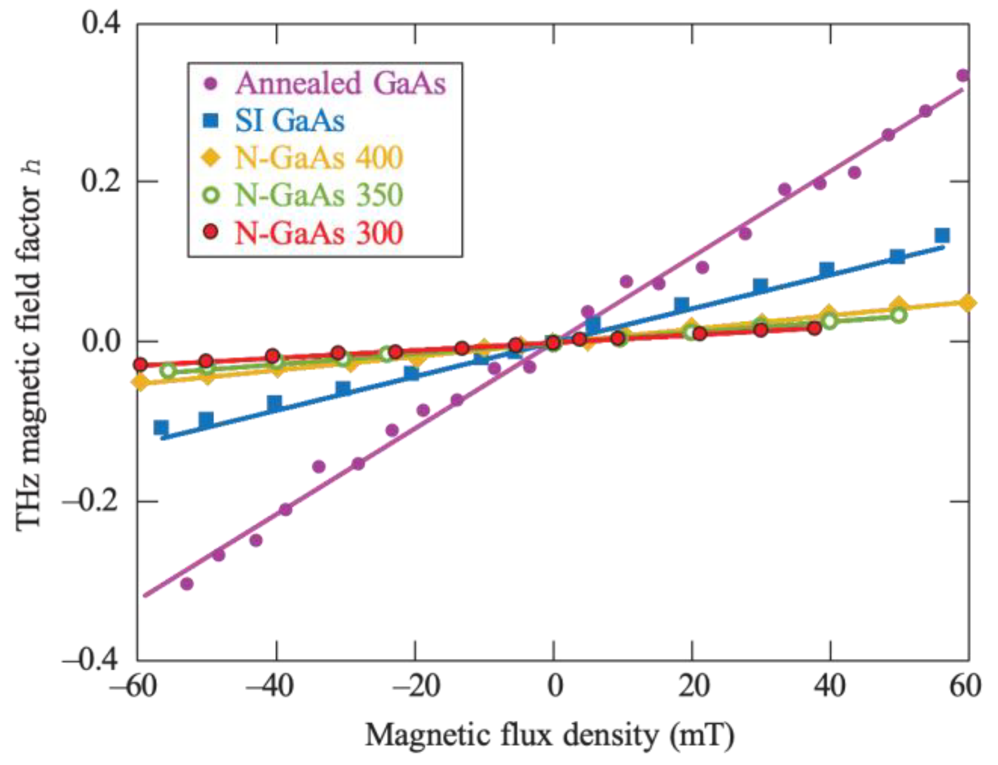
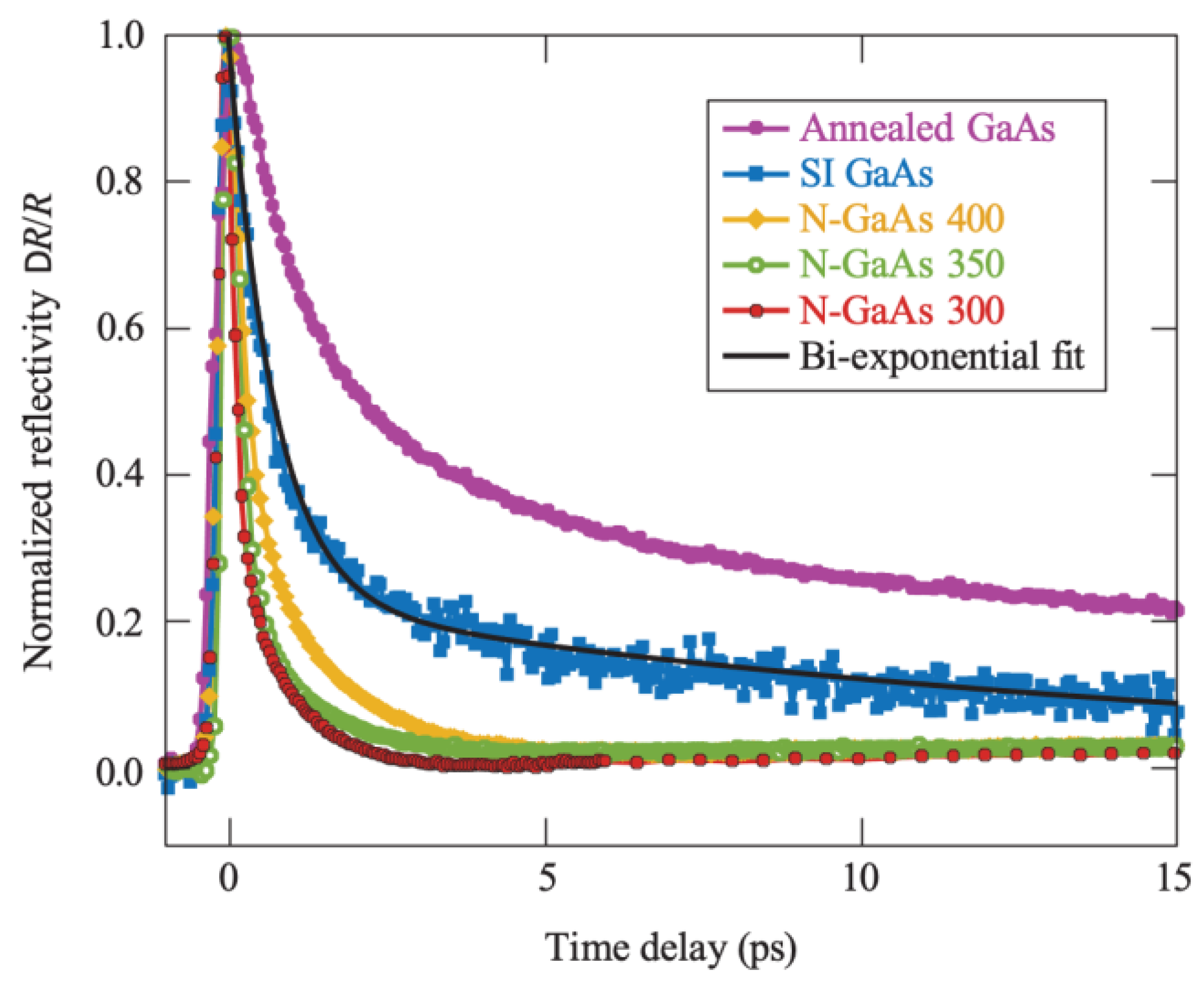
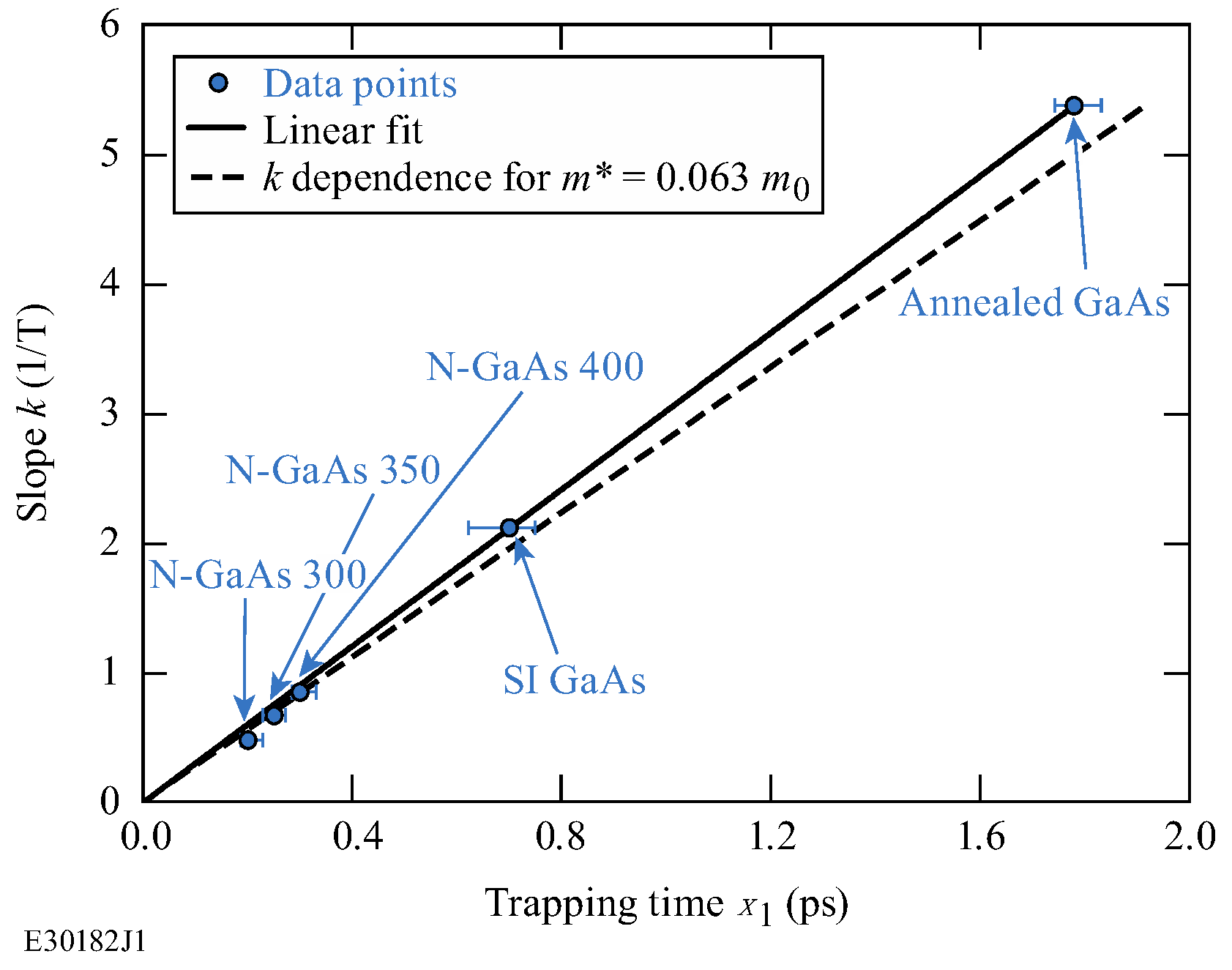
3. Results and Discussion

In highly resistive GaAs samples, the surface depletion field ED is perpendicular to the sample surface (along the x-axis, as shown in Figure 1, with B = 0) [3,16]. The latter stipulates that when the laser excitation is at normal incidence to the sample surface, no x-oriented (parallel to ED) electromagnetic signal can be detected, since our detector, in Figure 1, senses only the z-component of the THz transient. However, in all tested samples, we observed THz transients with an x-direction optical excitation. We first eliminated the possibility of the photo-Dember effect originating from the much faster diffusion velocities of the electrons than the holes, since the photo-Dember effect usually plays a dominant role in narrow band gap ( E G ) semiconductors; for example, InAs ( E G = 0.36 eV) and InSb ( E G = 0.1 eV), which exhibit a relatively weak depletion field, a short absorption depth, and a high electron mobility [12,27,28]. In wider bandgap semiconductors, such as GaAs ( E G = 1.43 eV), the depletion field is strong, and the absorption depth is relatively long. Since the photo-Dember field is proportional to the density gradient of the carriers [4], the contribution of the photo-Dember effect is expected to be negligible. Thus, the physical origin of transient THz emissions from GaAs samples excited at the normal optical incident angle must the optical rectification (OR) effect [27,29,30], Indeed, by rotating the SI GaAs sample in-plane (yz-plane), while maintaining the optical incidence at the normal angle, we observed, as shown in Figure 2, a very pronounced E z T H z angular dependence with the trifold (120°) symmetry characteristic of the OR signal from GaAs [29]. Our other samples also show the trifold symmetry, although, due to their small sizes, signals from N-implanted samples were quite noisy and are not shown here.
To observe the THz transient radiation emitted due to the surface ED field, unobstructed by the OR effect, we rotated each sample in yz-plane until their OR-related THz transient signal at the detector was negligible. In addition, we tilted the sample to an angle β , as shown in Figure 3. Under this arrangement, the ED field was also tilted, with a projection onto the z-axis that could be sensed by our THz detector. Since laser-induced carriers respond to the built-in ED field (assumed uniform), the β-dependent THz transient amplitude E z T H z ( β ) can be expressed as:
E z T H z ( β ) a z = q m * E D sin β
where a z is the z-component of the electron acceleration vector, m* is the GaAs electron effective mass, and q is the elementary charge. In Equation (1), we did not take into account the motion of holes, because of their heavy effective mass.
An example of the THz detector signal amplitude E z T H z ( β ) (dots) as a function of tilt angle β for an SI GaAs sample is presented in Figure 4. We observe that the increase in E z T H z ( β ) very accurately follows the sin β dependence predicted by Equation (1) up to the vicinity of the Brewster’s angle (~70°), where it quickly starts to drop due to the total reflection of the THz wave in GaAs. The above result was also observed in the other samples and can be explained as the THz transient emission due to the acceleration of photoelectrons driven by the ED field [3].
Next, we studied the amplitude dependence of THz transients emitted by our GaAs samples only due to the applied, external, and uniform magnetic field B. As described above, we rotated our test samples in the yz-plane to eliminate OR-related THz radiation and, simultaneously, set β = 0 to exclude any signal directly related to ED. In this configuration (see Figure 1), the THz signal measured by our detector can only be related to the applied B field, since B generates the Lorentz force that bends the trajectory of photoelectrons moving in the E D field. The corresponding acceleration vector a for electrons can be written as
a = q m * ( E D + v × B ) ,
where v is the electron drift velocity vector. If we do not take into account the effect of saturation velocity of moving electrons and assume the initial drift velocity to be zero [16,17], the solution of the z-component of the time dependent acceleration from Equation (2) can be derived as
a z = E D q m * sin ( ω t )
where ω = q B / m * is a so-called cyclotron frequency and t is the average electron acceleration time. E D and B are the surface depletion electric field strength and the magnetic field strength, respectively. Under our measurement conditions, the maximum magnetic field we could reach was about ~50 mT, so the corresponding ω of an electron in GaAs was about 130 GHz. Since THz generation is an ultrafast phenomenon, the expected t should be in the sub-picosecond range, overall, leading to a small value of ω t . Thus, we can use the Taylor expansion of sin ( ω t ) and keep only the linear term. The resulting simple relationship between the B-dependent amplitude of a THz transient E z T H z ( B ) and the electron acceleration time can be written as
E z T H z ( B ) a z = E D ( q m * ) 2 B t .
Figure 5 presents experimental time-domain waveforms for several B values, again using an SI GaAs sample as an example.
Next, to quantify how the THz radiation is influenced by the external B field, we define a magnetic-field factor:
η ( B ) E z T H z ( B ) E z T H z    
as the ratio of B-field-induced, experimental peak amplitude value given by Equation (4) and shown in Figure 5 to the reference E z T H z   , i.e., the amplitude of THz transient resulting from the acceleration of carriers along the ED field in the zero B field. We stress that, in our experimental configuration with the PC detector aligned along the z-axis (see Figure 1), we cannot measure E z T H z directly. We can, however, extract E z T H z   as   E z T H z ( β = π 2 ) , based on Equation (1) and the configuration shown in Figure 3. From Equation (1), we obtain E z T H z q m * E D , and substituting it into Equation (5), using Equation (4), we obtain the final relationship for η vs. B:
η ( B ) E z T H z ( B ) E z T H z     = E D ( q m * ) 2 B t q m * E D = q m * B t ,
where we assumed that, for an optimized and fixed experimental setup, proportionality constants between a z ’s and the amplitudes of THz transients (see Equations (1) and (4)) remain the same and cancel out in Equation (6).
Experimental η ( B ) dependencies, for all our tested samples, are presented in Figure 6. In this figure, for each sample, we plotted E z T H z ( B ) maxima (minima for negative Bs) of experimental time-domain waveforms such as the ones shown in Figure 5 for the corresponding B values, divided by E z T H z = E z T H z ( β = π 2 ) , the values obtained from plots like the one shown in Figure 4, by extrapolating the sine function fit up to β = π/2. We note that the η ( B ) dependencies are linear, as predicted by Equation (6), with the slope k =   q   m * t and its unit is 1/T, or, equivalently, m2/(sV). We also note that N-GaAs samples exhibit the smallest slopes, as compared to the other two types of GaAs samples.
Finally, we need to determine the physical relationship between the average acceleration time of electrons t and the electron lifetime τ . All tested samples are ultra-high resistive materials, so t should correspond the electron trapping time [26], since t defines the time window within which electrons can be accelerated by the Lorentz force. To confirm this hypothesis, in Figure 7, we present experimental ΔR/R waveforms, measured using the earlier described F-PPS setup. It is established that, for optically thick samples, the Δ R / R time dependence follows the nonequilibrium carrier concentration dynamics and can be fitted with a bi-exponential relaxation expression [26]. From Δ R / R fits for each sample (see a black solid line in Figure 7 as an example), we extracted a sub-picosecond trapping time of hot electrons τ 1 and a relatively long electron–hole recombination time τ 2 [31,32]. For each sample, the fit was excellent, with the confidence >95%. The results are summarized in Table 1, together with the k values extracted from traces in Figure 6.
As expected, the three N-GaAs samples exhibit the shortest τ 1 = 0.20, 0.25, and 0.30 ps, respectively. This is understandable because these samples were subject to a high implantation dose and the annealing only weakly affected their trapping times. However, the longest τ 1 corresponds to the sample annealed at the highest temperature. An analogous situation is observed when comparing SI GaAs and Annealed GaAs samples, although here the impact of annealing is much more visible [33]. Apparently, in this case, annealing measurably improved the crystal quality.
Figure 8 shows the dependence k = q m * τ 1 , for all 5 types of GaAs samples (black dots) and reveals a universal linear relationship (black solid line). This indicates that average acceleration time t in Equations (4) and (6), for our samples, is the trapping time τ 1 . During t , the Lorentz force accelerates electrons before they are trapped by defect states. Therefore, a high density of defects/traps in a semiconductor, e.g., in case of the N-GaAs samples, leads to a very short carrier lifetime, which, in turn, limits the impact of the magnetic field on the amplitude of the THz transient.
The next conclusion from Figure 8 is that, within the linear fit presented in Figure 8, the effective mass m * = q k / τ 1 for all our samples is the same, and the extracted value is m * / m 0 = 0.059 ( m 0 is the electron mass), which is quite close to the value 0.063 accepted in the literature for GaAs single crystals [34], as illustrated by the dashed line corresponding to k dependence for m * m 0 = 0.063 . The latter is an interesting result and shows that, despite the large differences in the crystallinity of our test samples, the electron effective mass derived from our magnetic field experiments remains constant and is very close to the effective mass of electrons in GaAs with a perfect crystalline structure. The most plausible interpretation is that, in highly resistive GaAs, free carrier concentration is so low that it results in a very small modification to the electronic band structure. The largest deviation from the ideal m * value was observed for the Annealed GaAs sample. In this case, contrary to other samples, the clear distinction between trapping and recombination processes is somewhat difficult to establish, so it is likely that the Lorentz-based electron acceleration time is the weighted average of τ 1 and τ 2 .

4. Conclusions

We exhaustively analyzed mechanisms of transient THz signals emitted from highly resistive GaAs samples with different crystallinity, as excited by femtosecond optical pulses. Next, we aligned our experimental setup in such a way that we could observe only transient THz emissions caused by the action of an external, applied magnetic field on optically excited electrons. We observed that the magnetic field impacted the THz transient generation and the corresponding factor η was directly proportional to the applied B field. The slope of the η dependence was, in turn, directly proportional to the samples’ nonequilibrium trapping time, measured using the femtosecond optical pump–probe spectroscopy technique. The latter enabled us to determine that the electron effective mass m * / m 0 = 0.059 was about 6% smaller than the literature   m * / m 0 value for an ideal GaAs single crystal. The latter reveals that GaAs samples with different crystallinity, including highly defected N-implanted samples, due to their very low intrinsic carrier concentration, have an electronic band structure that is very close to the ideal crystal.

Author Contributions

Conceptualization, G.C., M.M., J.C. and R.S.; methodology, G.C., M.M., H.H., R.A., D.E.B. and I.K.; software, G.C., J.C. and D.C.; validation, I.K., H.H., R.A., C.M.S. and R.S.; formal analysis, G.C., M.M., J.C. and D.C.; investigation, G.C., M.M., J.C., D.C. and I.K.; resources, R.A., H.H., C.M.S. and R.S., data curation, R.S.; writing—original draft preparation, G.C., J.C. and D.C.; writing—review and editing, G.C. and R.S.; supervision, H.H., R.A., C.M.S. and R.S.; project administration, H.H., R.A. and R.S.; funding acquisition, H.H, C.M.S. and R.S. All authors have read and agreed to the published version of the manuscript.

Funding

Research in Rochester was funded in part by the National Science Foundation grant #1842712. The work at the Research Center Jülich was performed within JuSPARC (Jülich Short-Pulse Particle Acceleration and Radiation Center), a strategy project funded by the BMBF (German Federal Ministry of Education and Research).

Institutional Review Board Statement

Not applicable.

Informed Consent Statement

Not applicable.

Data Availability Statement

Experimental data are available upon request from the corresponding author.

Acknowledgments

The authors thank Charles Chimera for his assistance in the early phase of this work.

Conflicts of Interest

The authors declare no conflict of interest. The funders had no role in the design of the study; in the collection, analyses, or interpretation of data; in the writing of the manuscript, or in the decision to publish the results.

References

  1. Tonouchi, M. Cutting-edge terahertz technology. Nat. Photonics 2007, 1, 97–105. [Google Scholar] [CrossRef]
  2. Bacon, D.R.; Madéo, J.; Dani, K.M. Photoconductive emitters for pulsed terahertz generation. J. Opt. 2021, 23, 064001. [Google Scholar] [CrossRef]
  3. Zhang, X.C.; Hu, B.B.; Darrow, J.T.; Auston, D.H. Generation of femtosecond electromagnetic pulses from semiconductor surfaces. Appl. Phys. Lett. 1990, 56, 1011. [Google Scholar] [CrossRef]
  4. Zhang, X.C.; Auston, D.H. Optoelectronic measurement of semiconductor surfaces and interfaces with femtosecond optics. J. Appl. Phys. 1992, 71, 326. [Google Scholar] [CrossRef]
  5. Kersting, R.; Heyman, J.N.; Strasser, G.; Unterrainer, K. Coherent plasmons in n-doped GaAs. Phys. Rev. B 1998, 58, 4553. [Google Scholar] [CrossRef]
  6. Heyman, J.N.; Neocleous, P.; Hebert, D.; Crowell, P.A.; Müller, T.; Unterrainer, K. Terahertz emission from GaAs and InAs in a magnetic field. Phys. Rev. B 2001, 64, 085202. [Google Scholar] [CrossRef] [Green Version]
  7. Hwang, J.S.; Lin, H.C.; Lin, K.I.; Zhang, X.C. Terahertz radiation from InAlAs and GaAs surface intrinsic-N+ structures and the critical electric fields of semiconductors. Appl. Phys. Lett. 2005, 87, 121107. [Google Scholar] [CrossRef]
  8. Chuang, S.L.; Schmitt-Rink, S.; Greene, B.I.; Saeta, P.N.; Levi, A.F.J. Optical rectification at semiconductor surfaces. Phys. Rev. Lett. 1992, 68, 102. [Google Scholar] [CrossRef] [Green Version]
  9. Reid, M.; Cravetchi, I.V.; Fedosejevs, R. Terahertz radiation and second-harmonic generation from InAs: Bulk versus surface electric-field-induced contributions. Phys. Rev. B—Condens. Matter Mater. Phys. 2005, 72, 035201. [Google Scholar] [CrossRef] [Green Version]
  10. Liu, K.; Xu, J.; Yuan, T.; Zhang, X.C. Terahertz radiation from InAs induced by carrier diffusion and drift. Phys. Rev. B—Condens. Matter Mater. Phys. 2006, 73, 155330. [Google Scholar] [CrossRef]
  11. Mendis, R.; Smith, M.L.; Bignell, L.J.; Vickers, R.E.M.; Lewis, R.A. Strong terahertz emission from (100) p-type InAs. J. Appl. Phys. 2005, 98, 126104. [Google Scholar] [CrossRef] [Green Version]
  12. Reklaitis, A. Terahertz emission from InAs induced by photo-Dember effect: Hydrodynamic analysis and Monte Carlo simulations. J. Appl. Phys. 2010, 108, 053102. [Google Scholar] [CrossRef]
  13. Hasegawa, T.; Okushima, Y.; Tanaka, Y. Characteristics of terahertz wave emissions under the coexistence of different sub-picosecond transient phenomena in GaAs epitaxial films. Appl. Phys. Express 2021, 14, 041005. [Google Scholar] [CrossRef]
  14. Mangeney, J. THz Photoconductive Antennas Made From Ion-Bombarded Semiconductors. J. Infrared Millim. Terahertz Waves 2011, 33, 455–473. [Google Scholar] [CrossRef]
  15. Bhattacharya, A.; Bhattacharya, A.; Bhattacharya, A.; Ghindani, D.; Ghindani, D.; Prabhu, S.S. Enhanced terahertz emission bandwidth from photoconductive antenna by manipulating carrier dynamics of semiconducting substrate with embedded plasmonic metasurface. Opt. Express 2019, 27, 30272–30279. [Google Scholar] [CrossRef]
  16. Zhang, X.C.; Jin, Y.; Hewitt, T.D.; Sangsiri, T.; Kingsley, L.E.; Weiner, M. Magnetic switching of THz beams. Appl. Phys. Lett. 1993, 62, 2003. [Google Scholar] [CrossRef]
  17. Weiss, C.; Wallenstein, R.; Beigang, R. Magnetic-field-enhanced generation of terahertz radiation in semiconductor surfaces. Appl. Phys. Lett. 2000, 77, 4160. [Google Scholar] [CrossRef]
  18. Othonos, A. Probing ultrafast carrier and phonon dynamics in semiconductors. J. Appl. Phys. 1998, 83, 1789. [Google Scholar] [CrossRef]
  19. Kojima, O.; Tarui, Y.; Kita, T.; Majeed, A.; Ivanov, P.; Ivanov, P.; Clarke, E.; Hogg, R.A.; Hogg, R.A. Increase in terahertz-wave intensity in a magnetic field due to difference-frequency mixing by exciton excitation in a GaAs/AlAs multiple quantum well. Opt. Express 2022, 30, 11789–11796. [Google Scholar] [CrossRef]
  20. Grishkov, V.E.; Uryupin, S.A. Terahertz radiation generation in doped semiconductor interacting with femtosecond pulse in constant magnetic field. Laser Phys. Lett. 2022, 19, 116101. [Google Scholar] [CrossRef]
  21. Mikulics, M.; Marso, M.; Kordoš, P.; Stanček, S.; Kováč, P.; Zheng, X.; Wu, S.; Sobolewski, R. Ultrafast and highly sensitive photodetectors fabricated on high-energy nitrogen-implanted GaAs. Appl. Phys. Lett. 2003, 83, 1719. [Google Scholar] [CrossRef] [Green Version]
  22. Mikulics, M.; Marso, M.; Mayorga, I.C.; Güsten, R.; Stanček, S.; Kováč, P.; Wu, S.; Li, X.; Khafizov, M.; Sobolewski, R.; et al. Photomixers fabricated on nitrogen-ion-implanted GaAs. Appl. Phys. Lett. 2005, 87, 041106. [Google Scholar] [CrossRef] [Green Version]
  23. Adam, R.; Chen, G.; Bürgler, D.E.; Shou, T.; Komissarov, I.; Heidtfeld, S.; Hardtdegen, H.; Mikulics, M.; Schneider, C.M.; Sobolewski, R. Magnetically and optically tunable terahertz radiation from Ta/NiFe/Pt spintronic nanolayers generated by femtosecond laser pulses. Appl. Phys. Lett. 2019, 114, 212405. [Google Scholar] [CrossRef]
  24. Geižutis, A.; Krotkus, A.; Bertulis, K.; Molis, G.; Adomavičius, R.; Urbanowicz, A.; Balakauskas, S.; Valaika, S. Terahertz radiation emitters and detectors. Opt. Mater. 2008, 30, 786–788. [Google Scholar] [CrossRef]
  25. Zhang, J.; Belousov, A.; Karpiski, J.; Batlogg, B.; Wicks, G.; Sobolewski, R. Time-resolved femtosecond optical characterization of multi-photon absorption in high-pressure-grown Al0.86Ga0.14N single crystals. J. Appl. Phys. 2011, 110, 113112. [Google Scholar] [CrossRef]
  26. Serafini, J.; Akbas, Y.; Crandall, L.; Bellman, R.; Williams, C.K.; Sobolewski, R. Time-resolved, nonequilibrium carrier dynamics in Si-on-glass thin films for photovoltaic cells. Semicond. Sci. Technol. 2016, 31, 045006. [Google Scholar] [CrossRef]
  27. Gu, P.; Tani, M.; Kono, S.; Sakai, K.; Zhang, X.C. Study of terahertz radiation from InAs and InSb. J. Appl. Phys. 2002, 91, 5533. [Google Scholar] [CrossRef] [Green Version]
  28. Dekorsy, T.; Auer, H.; Bakker, H.; Roskos, H.; Kurz, H. THz electromagnetic emission by coherent infrared-active phonons. Phys. Rev. B 1996, 53, 4005. [Google Scholar] [CrossRef] [PubMed] [Green Version]
  29. Rice, A.; Jin, Y.; Ma, X.F.; Zhang, X.C.; Bliss, D.; Larkin, J.; Alexander, M. Terahertz optical rectification from 〈110〉 zinc-blende crystals. Appl. Phys. Lett. 1998, 64, 1324. [Google Scholar] [CrossRef]
  30. Wu, X.; Xu, X.; Lu, X.; Wang, L. Terahertz emission from semi-insulating GaAs with octadecanthiol-passivated surface. Appl. Surf. Sci. 2013, 279, 92–96. [Google Scholar] [CrossRef]
  31. Hall, R.N. Electron-Hole Recombination in Germanium. Phys. Rev. 1952, 87, 387. [Google Scholar] [CrossRef]
  32. Shockley, W.; Read, W.T. Statistics of the Recombinations of Holes and Electrons. Phys. Rev. 1952, 87, 835. [Google Scholar] [CrossRef]
  33. Mikulics, M.; Hardtdegen, H.; Adam, R.; Grützmacher, D.; Gregušová, D.; Novák, J.; Kordoš, P.; Sofer, Z.; Serafini, J.; Zhang, J.; et al. Impact of thermal annealing on nonequilibrium carrier dynamics in single-crystal, freestanding GaAs mesostructures. Semicond. Sci. Technol. 2014, 29, 045022. [Google Scholar] [CrossRef]
  34. Gottstein, G.; Goerdeler, M.; Prasad, G.V.S.S. Encyclopedia of Condensed Matter Physics; Elsevier: Amsterdam, The Netherlands, 2005. [Google Scholar]
Figure 1. Schematics of the basic experimental geometry. The surface of the sample is parallel to the yz-plane. The built-in depletion electric field ED is along the x-axis and perpendicular to the sample surface. A lens is used to focus a laser beam at the surface of the sample, and a Teflon lens placed after the sample collimates the emitted THz radiation towards a PC THz detector aligned in such a way that it can only sense the z-component of the THz transient. An external magnetic, field applied along the y-axis, was used in the B-field enhancement experiments.
Crystals 12 01635 g001
Figure 2. THz amplitude dependence of the azimuthal angle showing a trifold (120°) symmetry indicate the optical rectification THz emission.
Crystals 12 01635 g002
Figure 3. Variation in the basic experimental geometry with the sample tilted by an angle β with respect to the z-axis. The built-in ED field is no longer aligned along the x-axis, so it has a projection Ez that can be captured by the PC THz detector.
Crystals 12 01635 g003
Figure 4. THz transient amplitude dependence on the tilt angle β for a SI GaAs sample (dots). The fit (solid line) corresponds to the sine function in accordance with Equation (1). The drop in THz amplitude at ~70° (Brewster’s angle) is due to the total reflection of the THz wave in GaAs. Results for other samples are not shown, but they exhibit the same behavior.
Crystals 12 01635 g004
Figure 5. Amplitudes of THz transients emitted from a SI GaAs sample at different strengths of the external magnetic field with normal incident angle of the excitation beam and zero optical rectification. Results for other samples are not shown, but they exhibit the same behavior.
Crystals 12 01635 g005
Figure 6. Magnetic-field factor η of transient THz amplitudes vs. the magnetic flux density for all five GaAs samples used in the study. Dots are experimental datapoints collected from every sample (see the text) and solid lines are the corresponding best linear fits.
Crystals 12 01635 g006
Figure 7. Normalized Δ R / R waveforms of all five samples. The experimental data are shown as dots, and the bi-exponential fit is presented as a solid black line for a SI GaAs sample as an example. Each sample was tested on at least three different spots to eliminate any influence of sample inhomogeneities.
Crystals 12 01635 g007
Figure 8. Dependence of the slope k dependence on the trapping time τ 1 . The dots are experimental data points, and a black line is the best linear fit yielding m * / m 0 = 0.059 . The dashed line corresponds to the k dependence for m * / m 0 = 0.063 , the literature value for GaAs [34].
Crystals 12 01635 g008
Table 1. Data of the slope k, the trapping time τ 1 , and the electron–hole recombination time τ 2 . k values were extracted from Figure 6 as linear fits, while the time constants were obtained by applying a bi-exponential fit to each experimental pump–probe waveform presented in Figure 7. Error margins in the τ 1 column correspond to the range of fitting coefficients within the >95% confidence bounds.
Samplek (1/T)τ1 (ps)τ2 (ps)
Annealed GaAs5.381.74 (−0.04; +0.06)35.00
SI GaAs2.120.70 (−0.08; +0.05)16.00
N-GaAs 4000.850.30 (−0.01; +0.03)1.40
N-GaAs 3500.670.25 (−0.02; +0.02)1.23
N-GaAs 3000.480.20 (−0.01; +0.03)1.30
Publisher’s Note: MDPI stays neutral with regard to jurisdictional claims in published maps and institutional affiliations.

