
A Review on Precision Polishing Technology of Single-Crystal SiC


Abstract
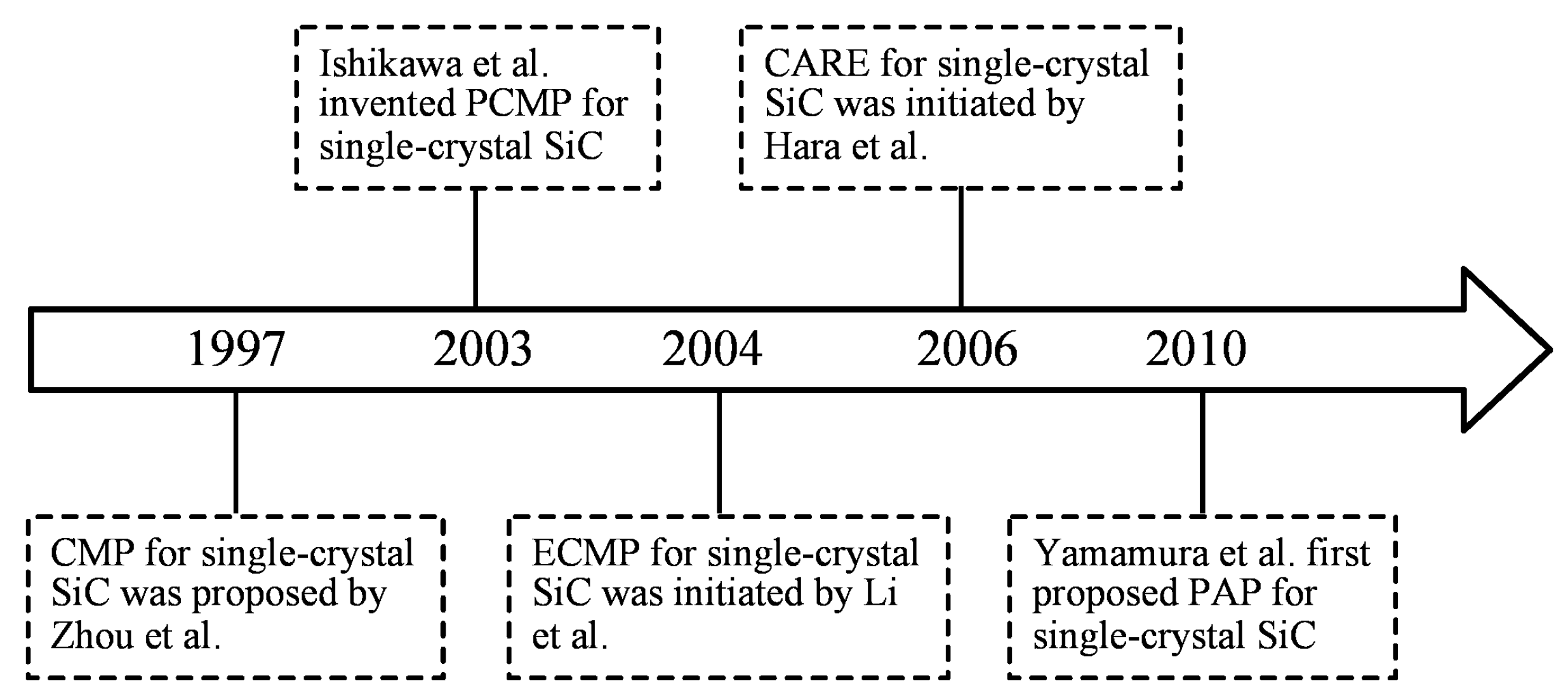
:1. Introduction
2. The Main Precision Polishing Technologies of Single-Crystal SiC
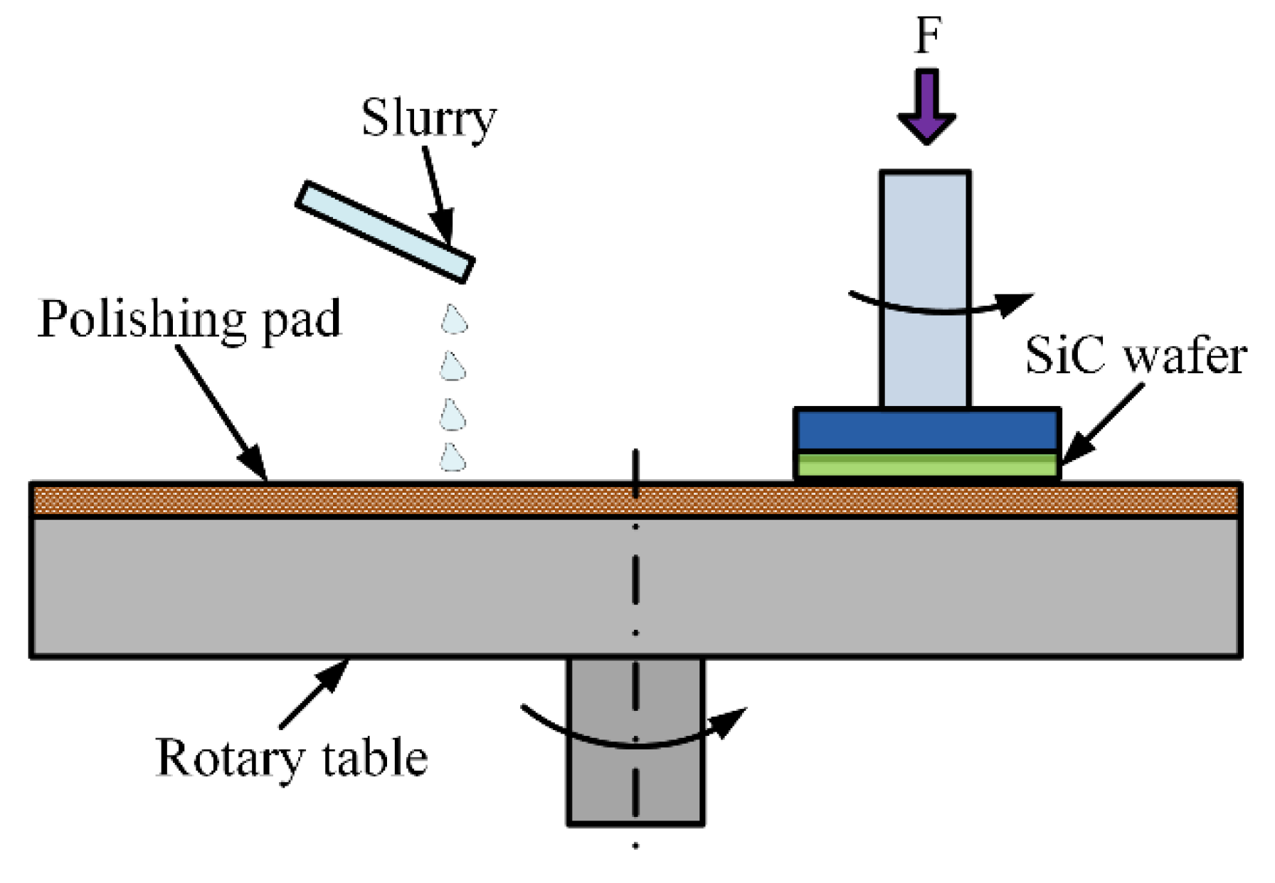
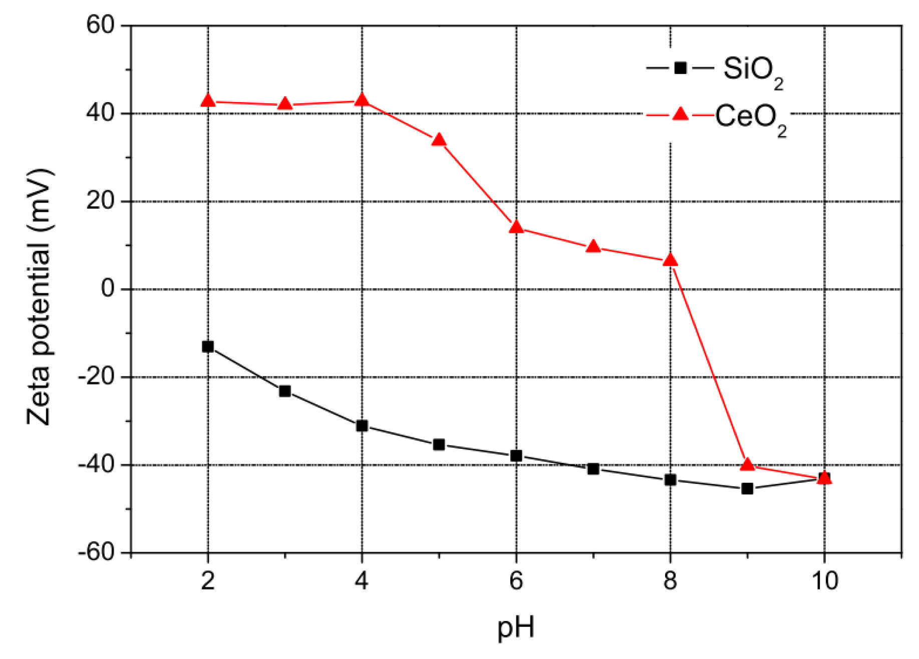
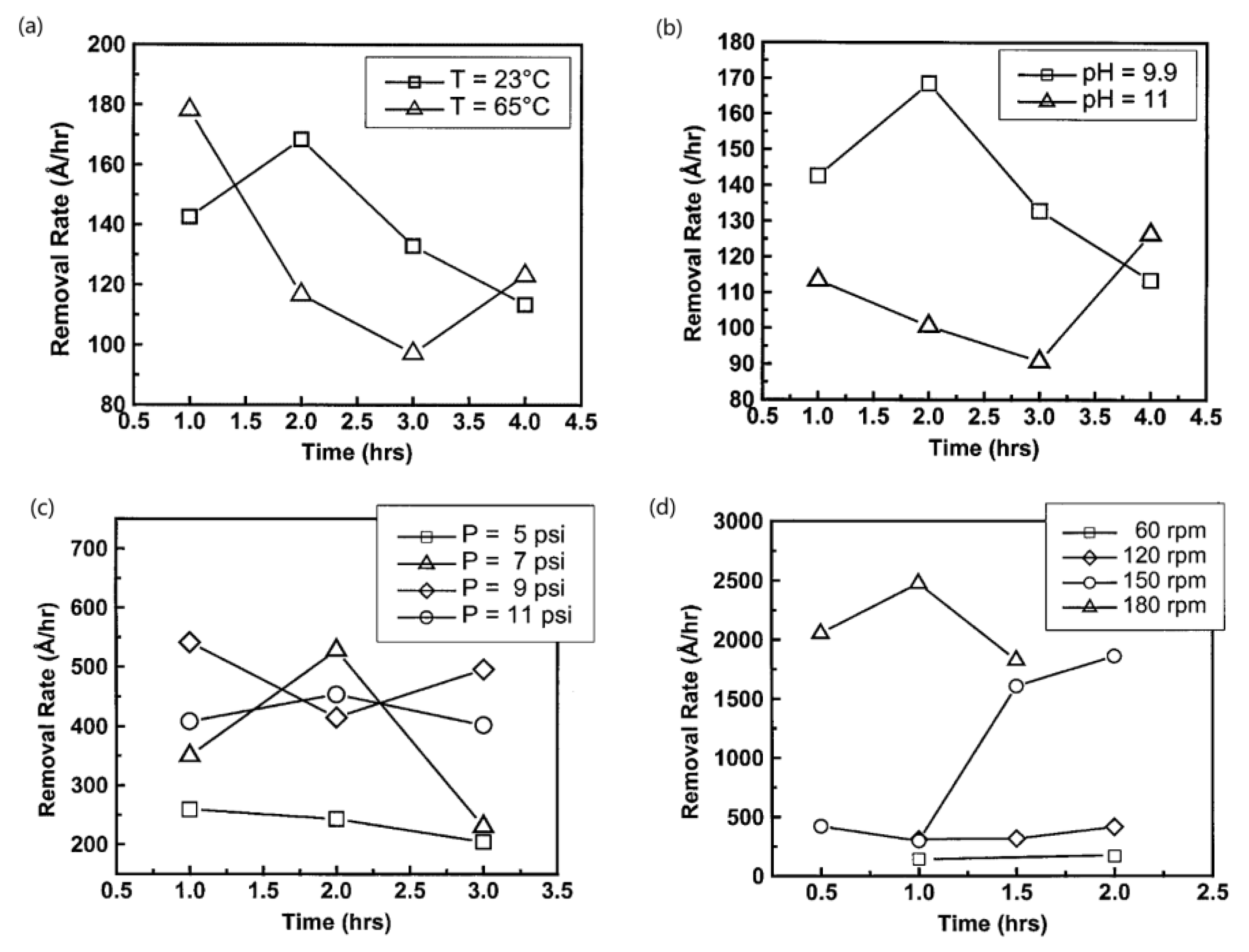
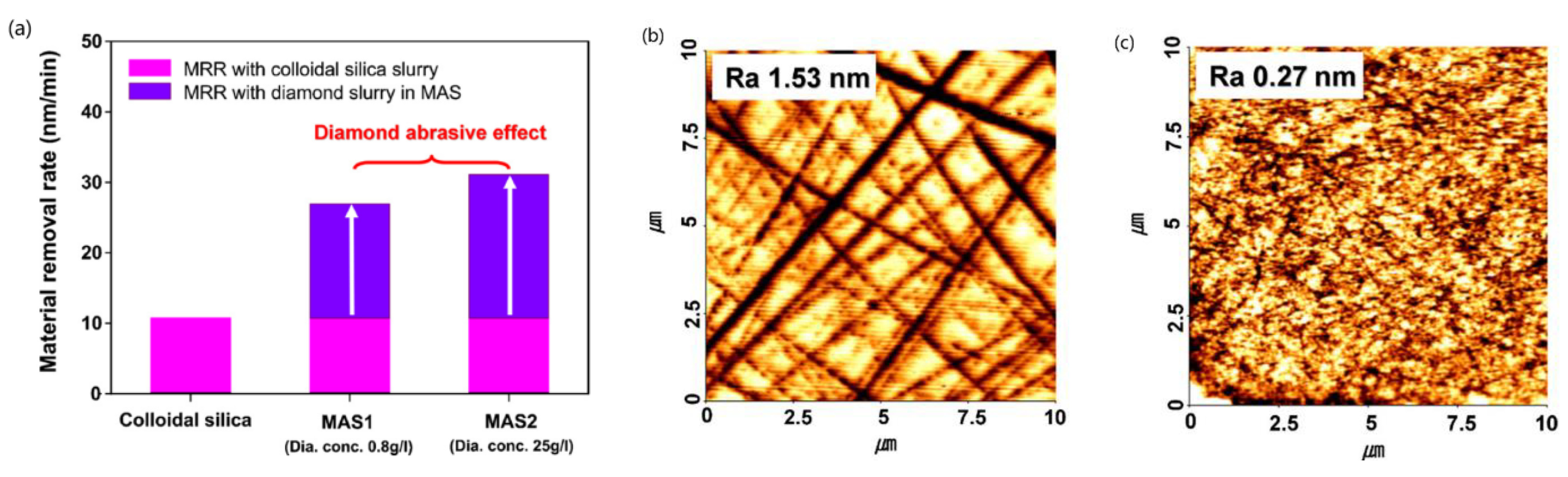
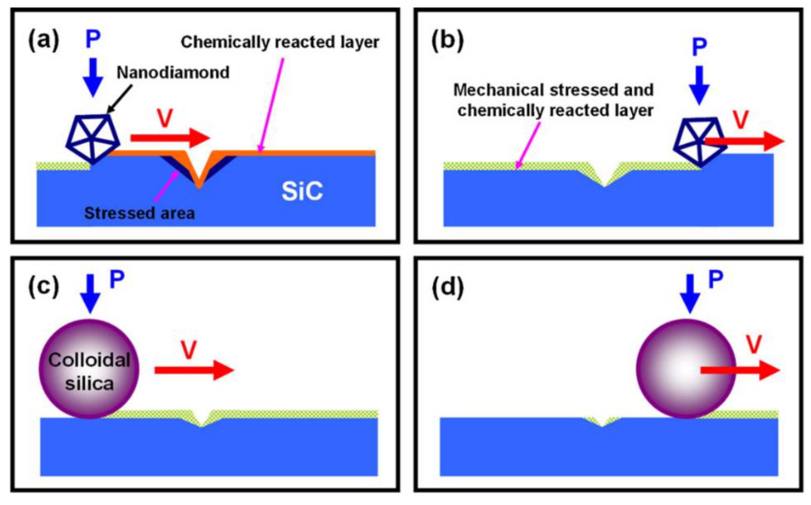
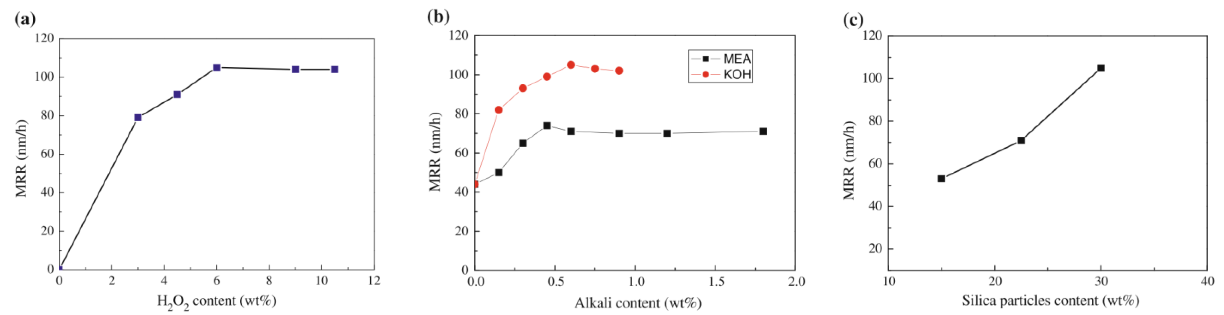
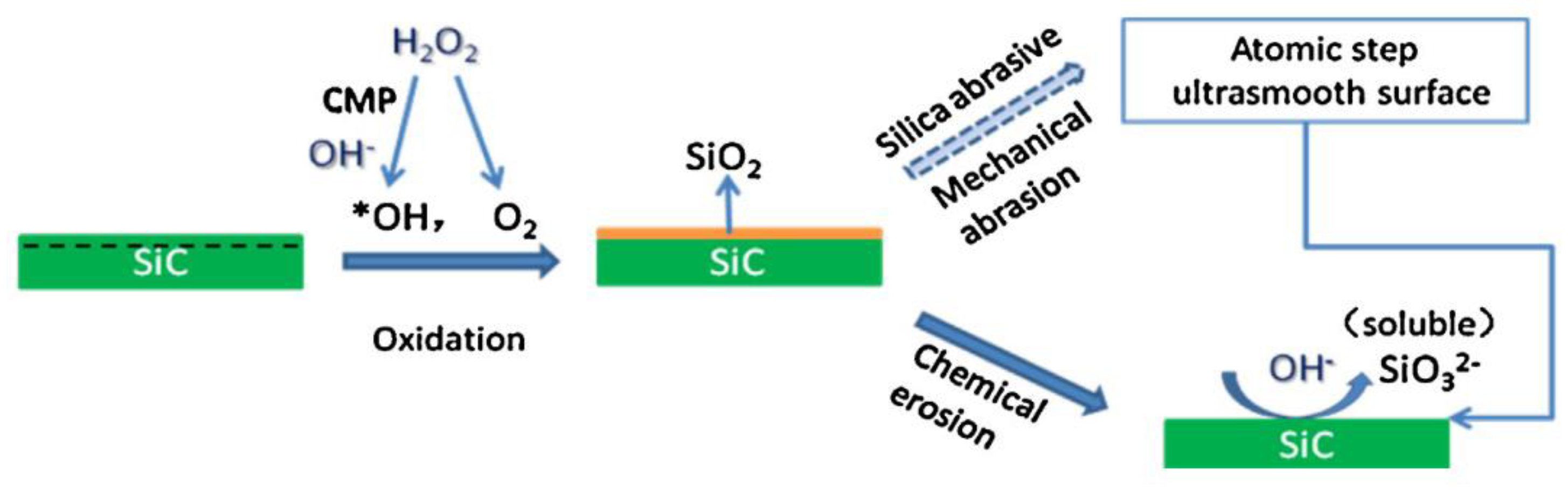
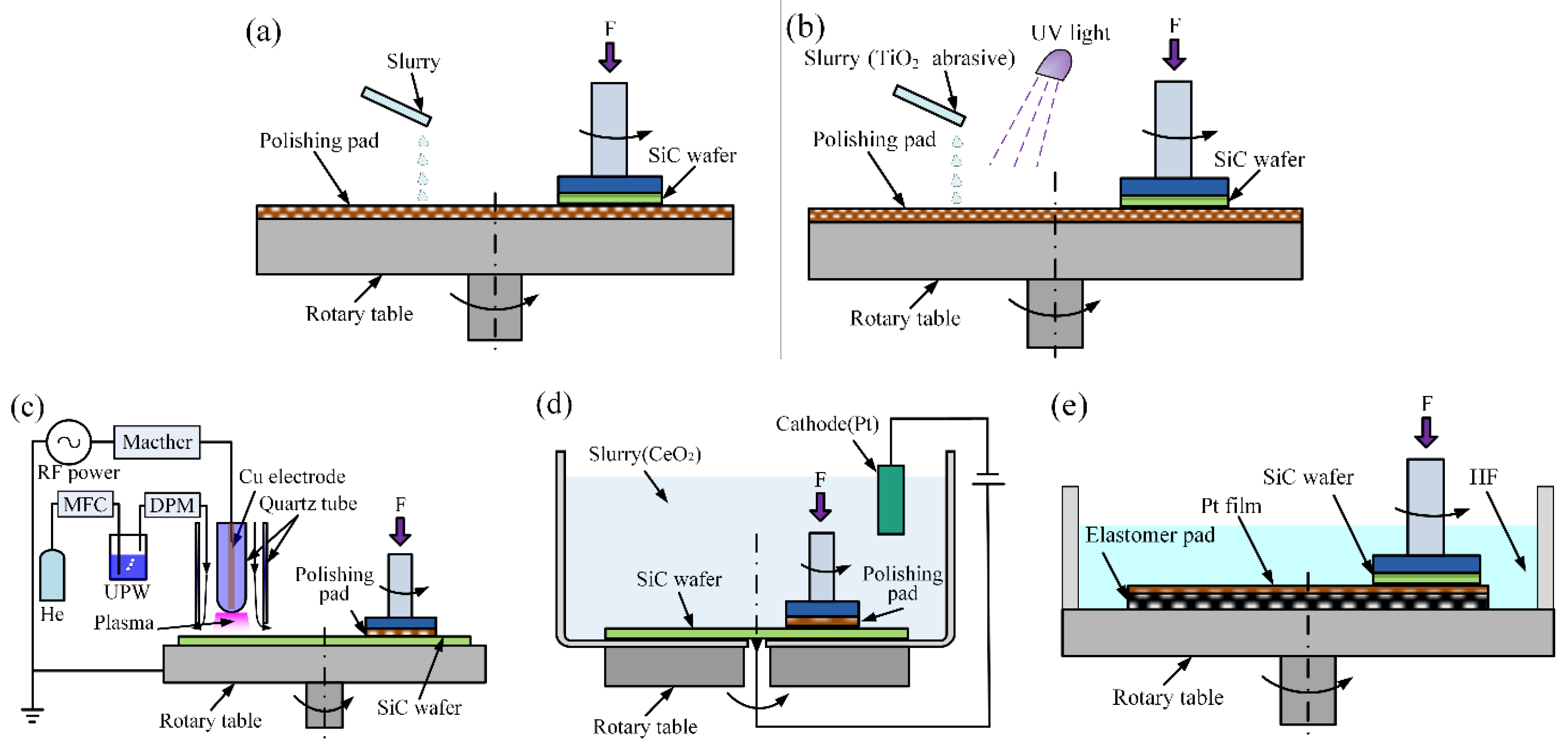
2.1. Chemical Mechanical Polishing (CMP)
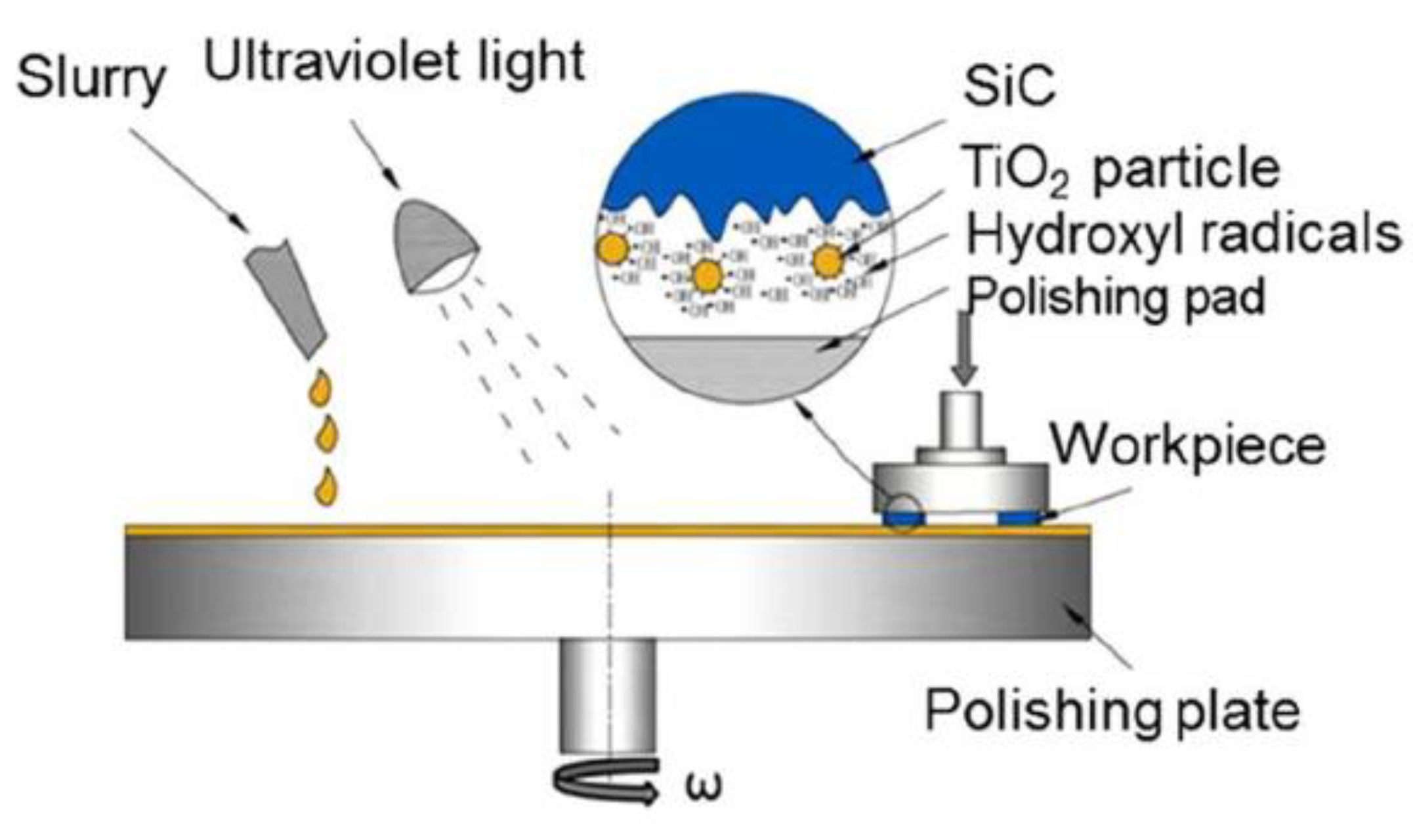
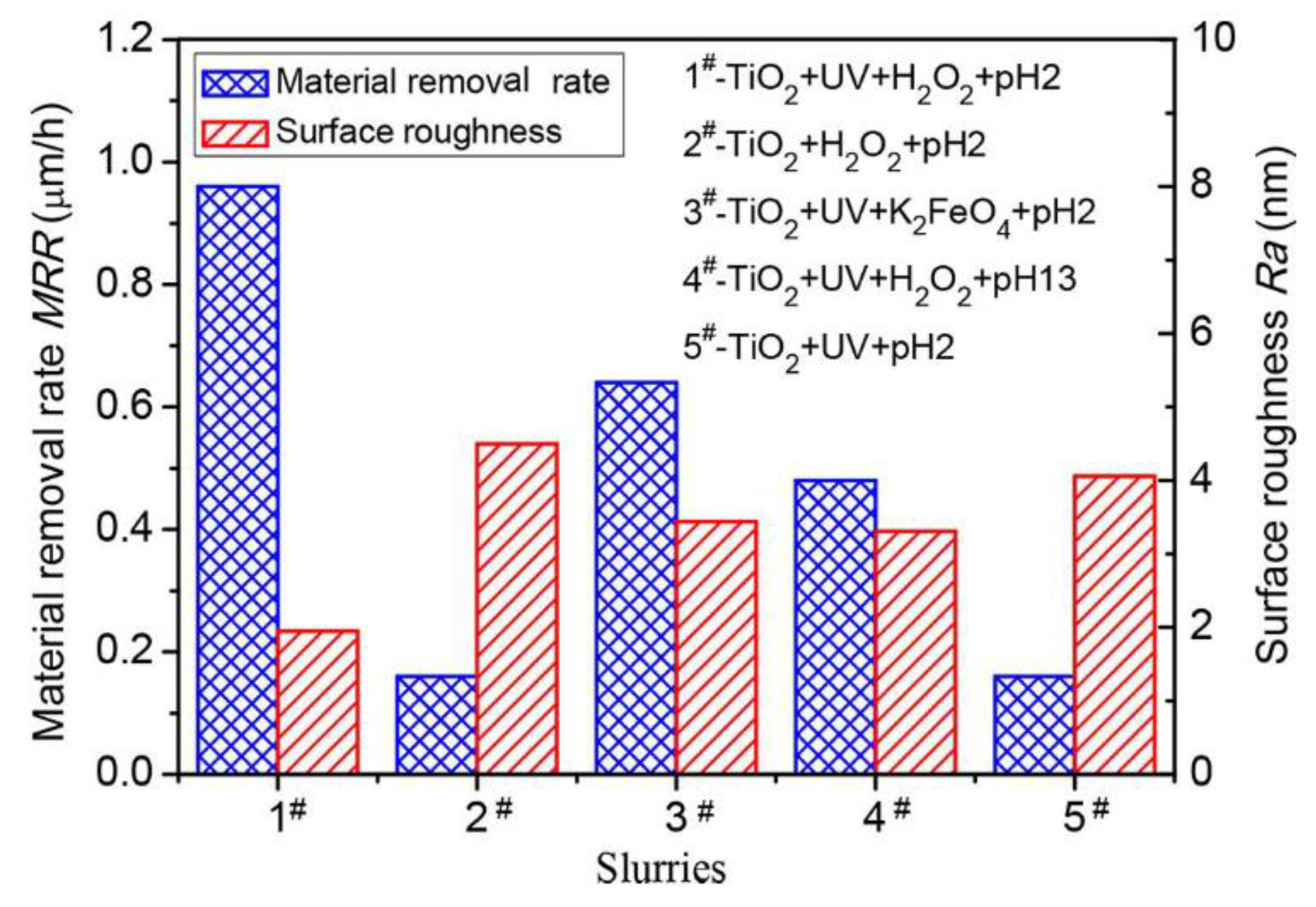
2.2. Photocatalytic Chemical Mechanical Polishing (PCMP)
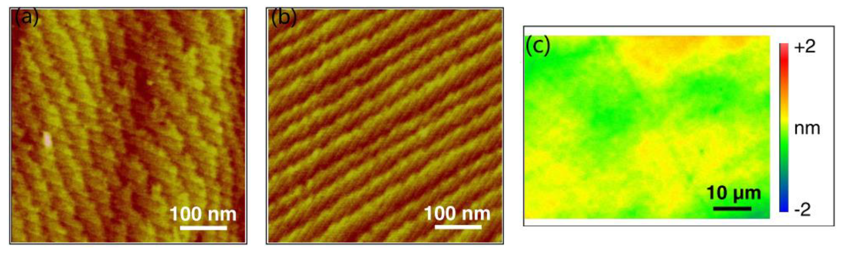
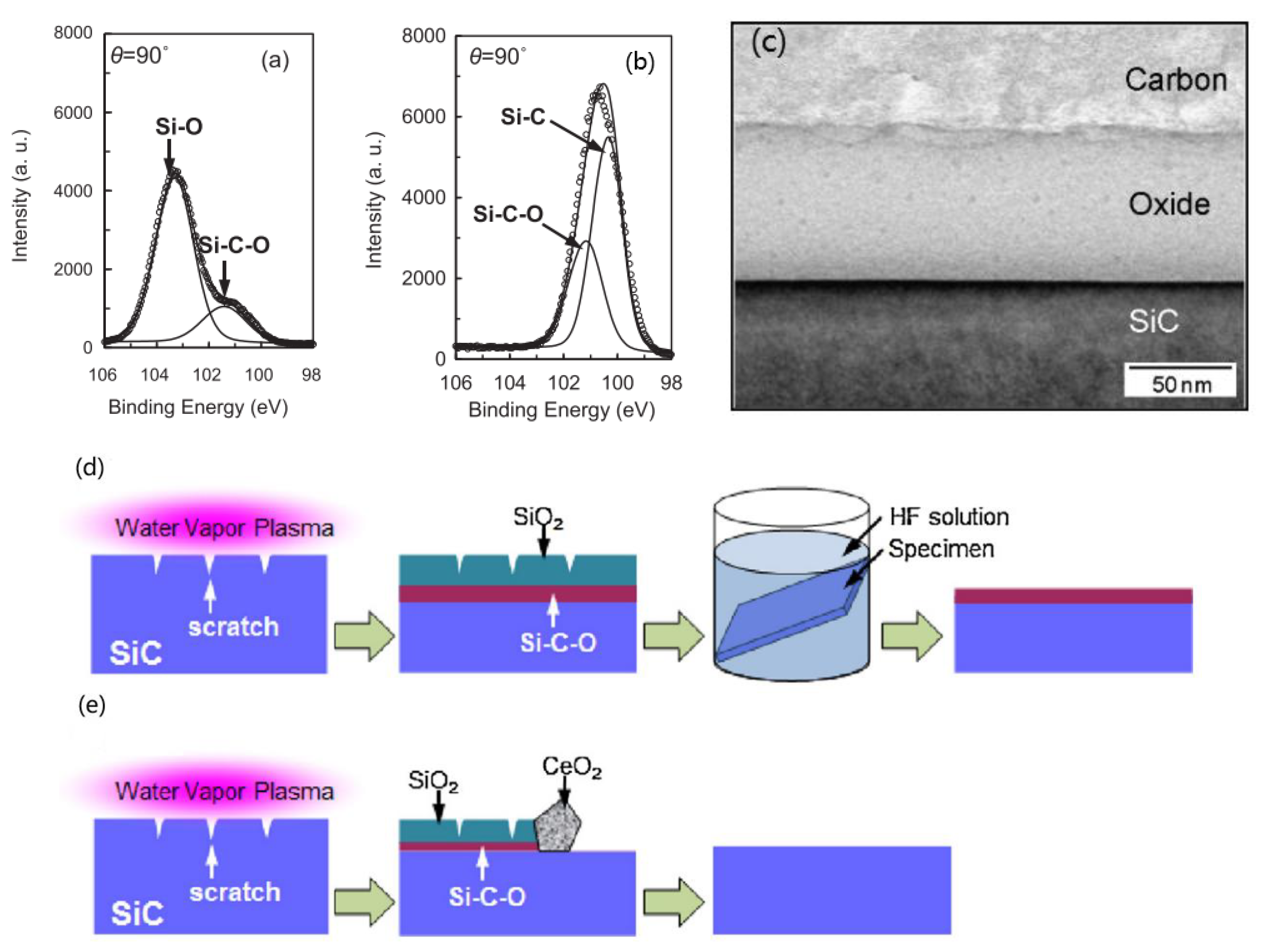
2.3. Plasma-Assisted Polishing (PAP)
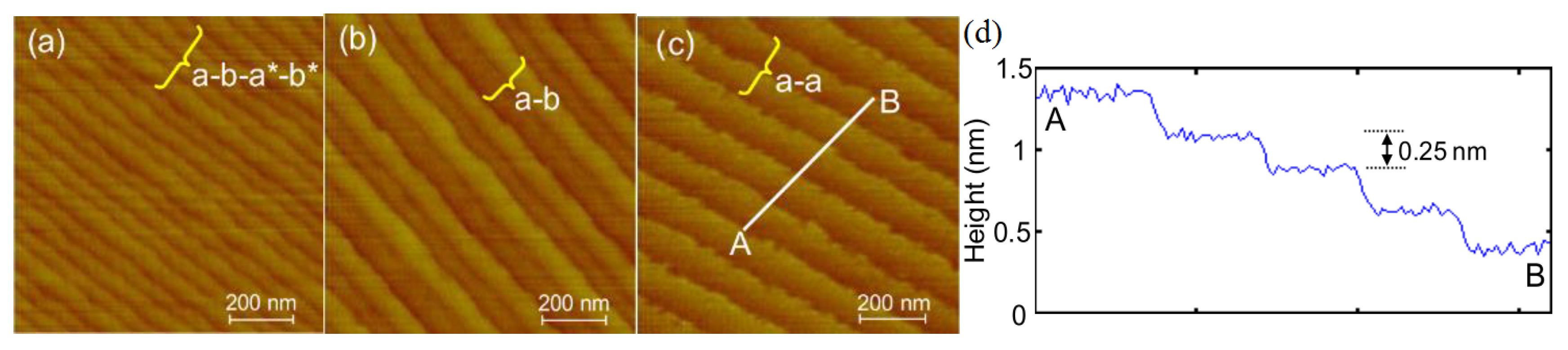
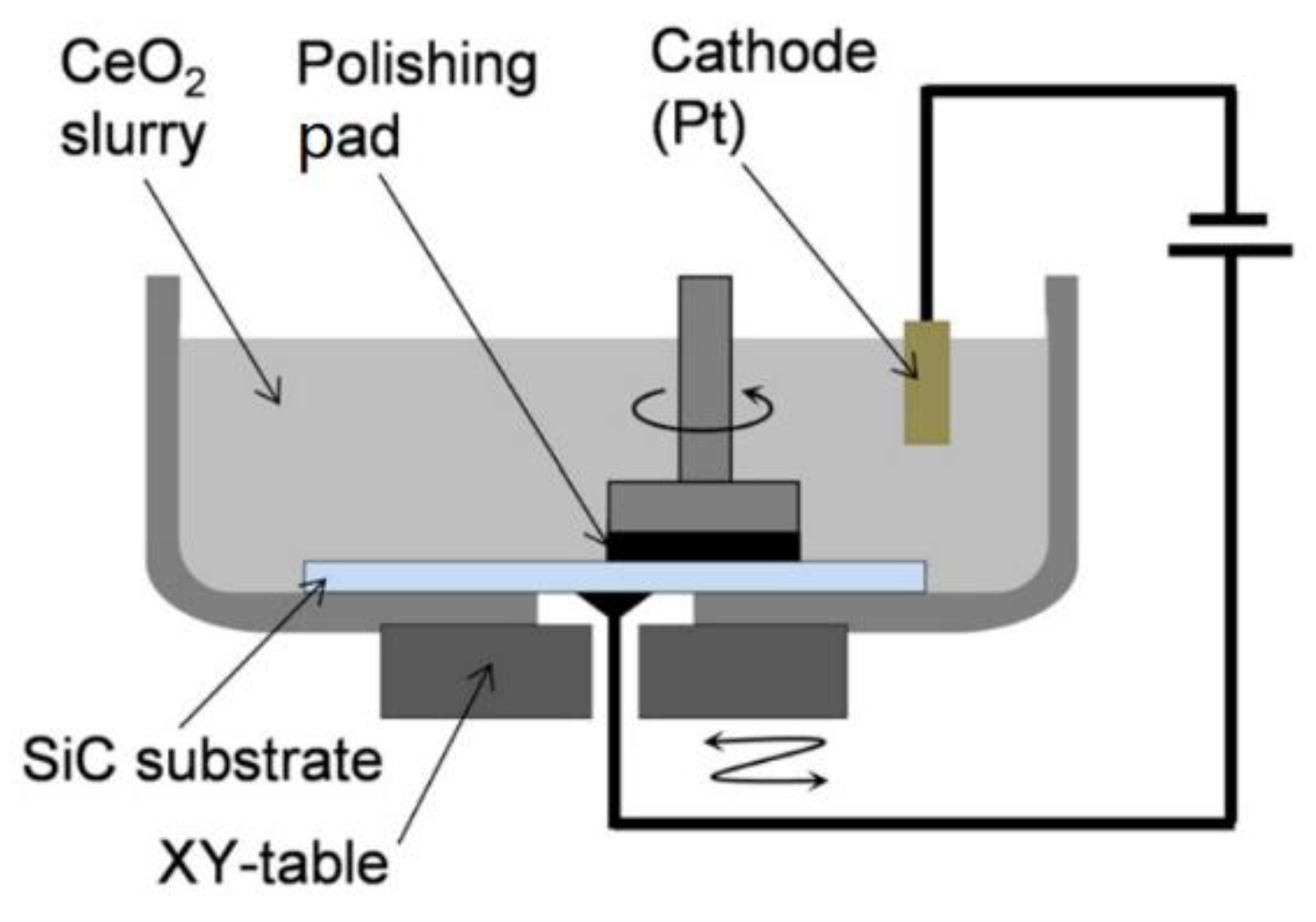
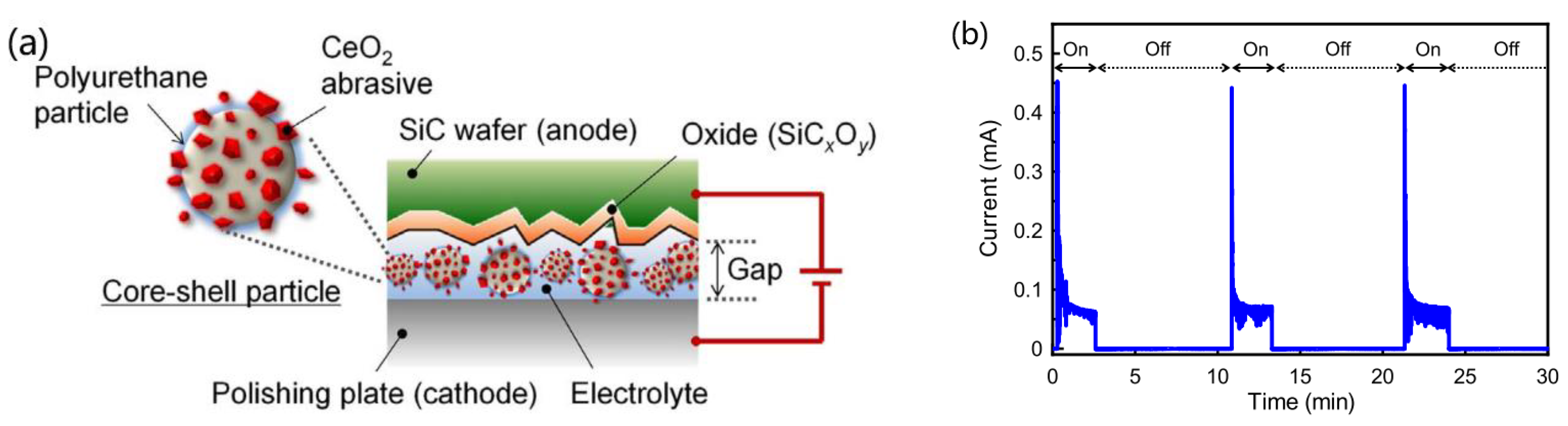
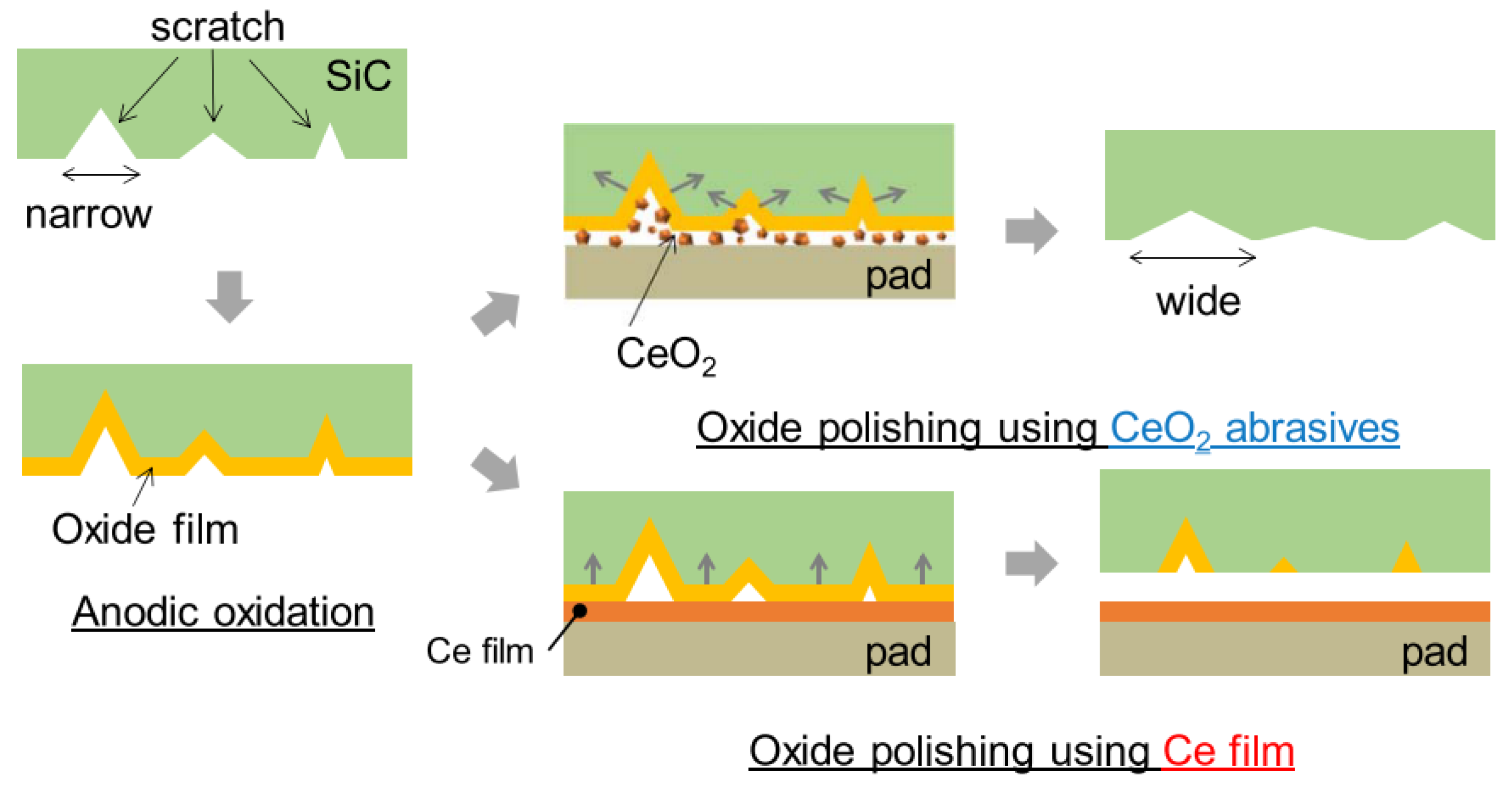
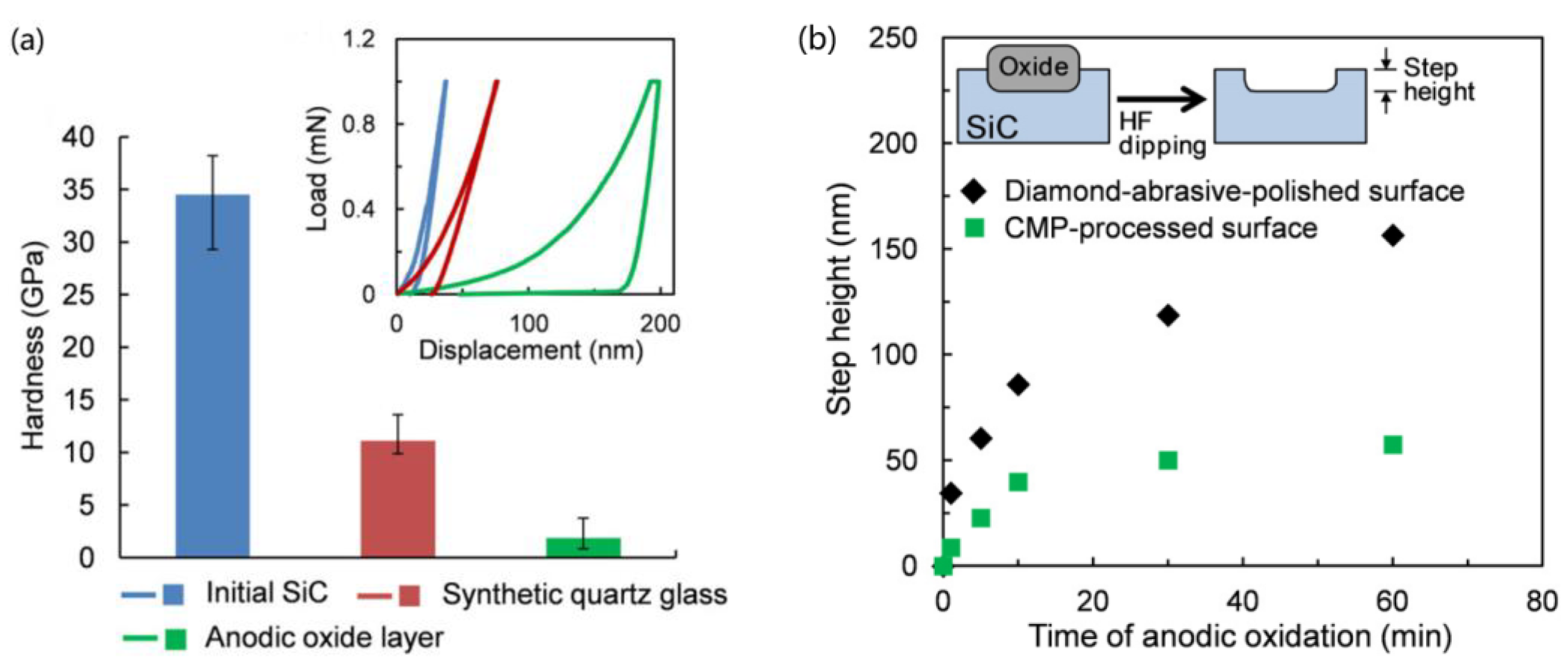
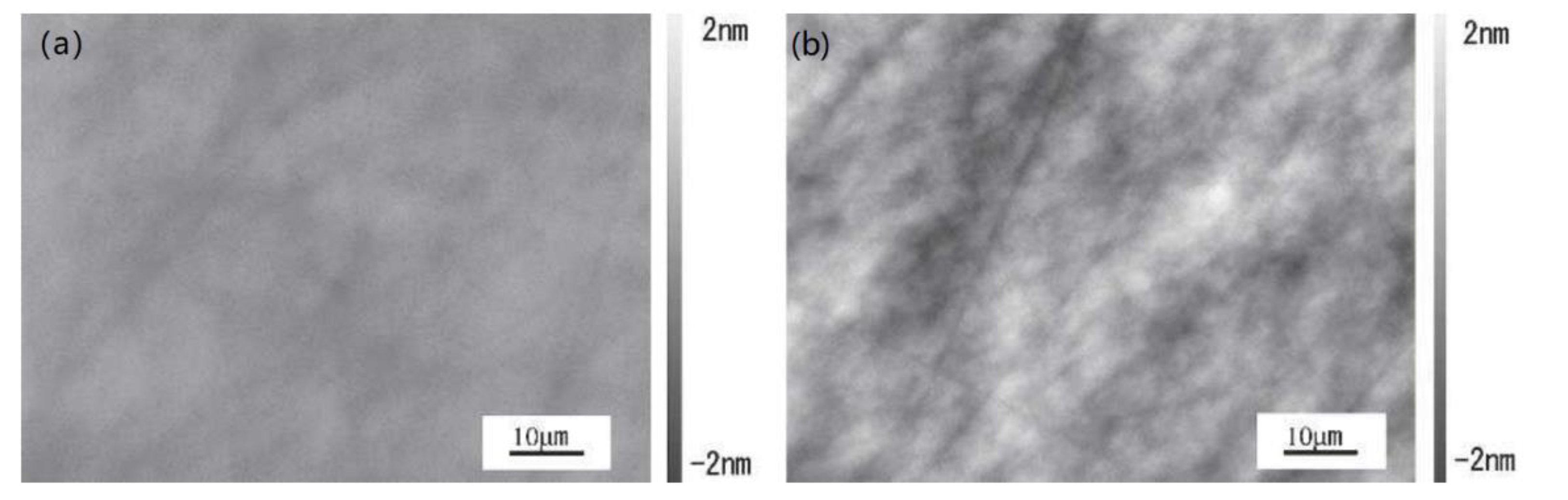
2.4. Electrochemical Mechanical Polishing (ECMP)
- (1)
- Unoxidized state (ab): the anodic oxidation did not occur since no current flowed;
- (2)
- Active state (bc): the anodic oxidation began to occur when the voltage increased into the active stage;
- (3)
- Passive state (cd): the oxidation reaction was hindered by the passive film due to the increase in the thickness of oxide film;
- (4)
- Transient state (de): the oxide protrusions were generated by the breakdown of the passive film;
- (5)
- Transpassive state (ef): as the voltage continued to rise, the current increased with the increasing of the voltage and entered into the transpassive state. The oxide protrusions were introduced between the transient state and the transpassive state.
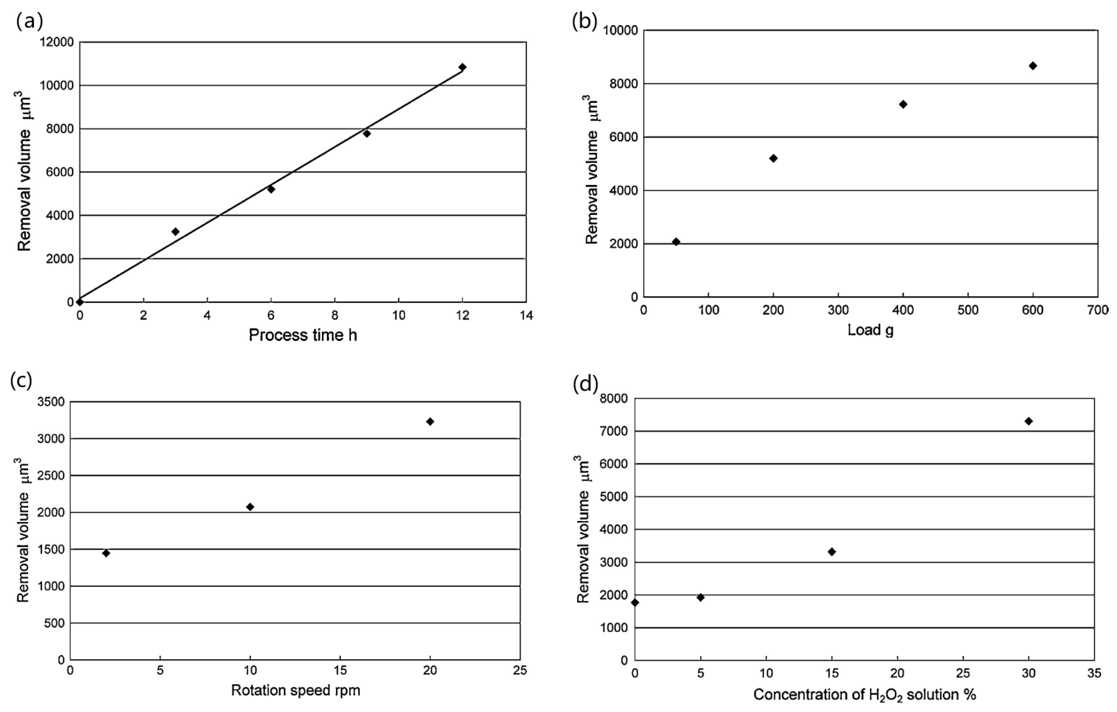
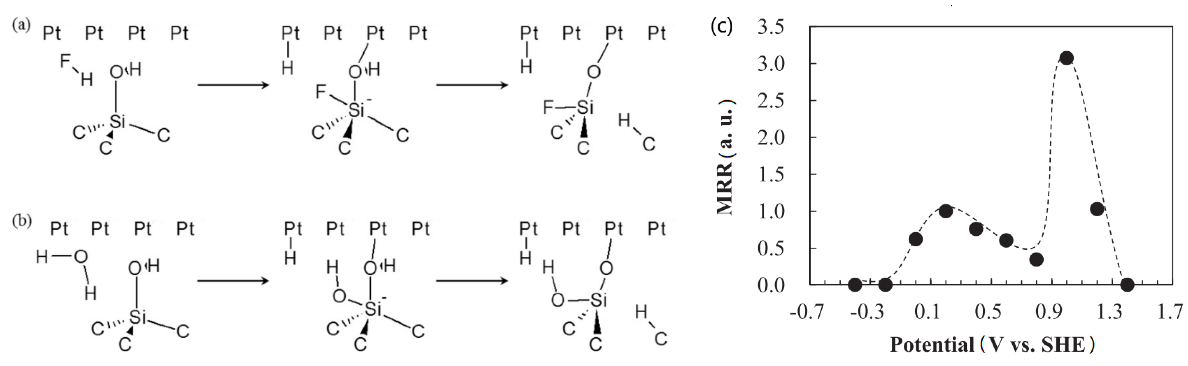
2.5. Catalyst-Referred Etching (CARE)
3. Comparison of the Main Precision Polishing Technologies
3.1. Experimental Setup
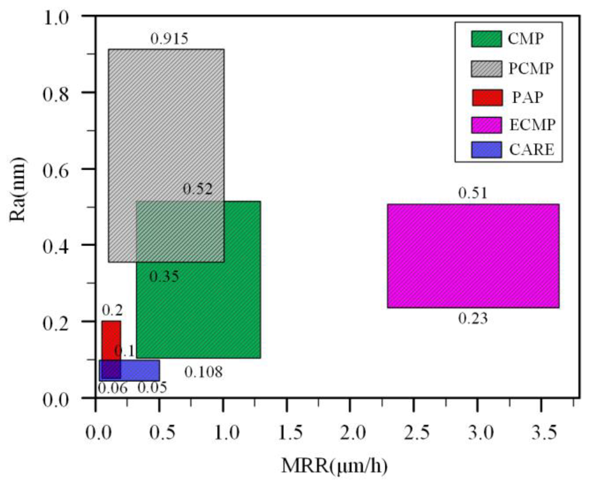
3.2. Material Removal Rate (MRR) and Surface Roughness
4. Other Probable Enhancement Polishing Technologies for Single-Crystal SiC
4.1. Ultrasonic Vibration-Assisted Polishing
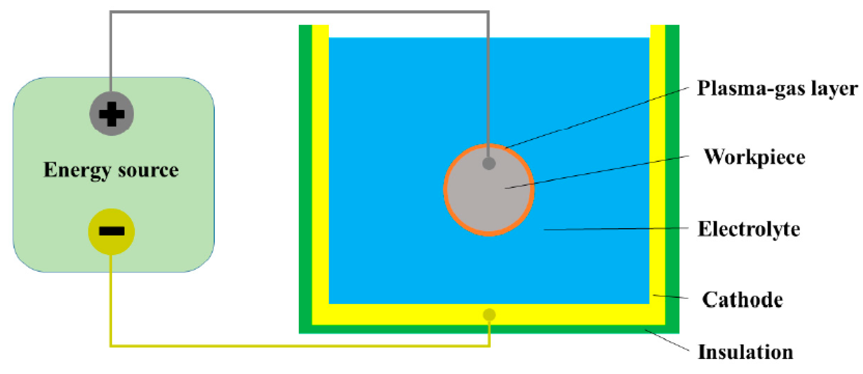
4.2. Electrolyte Plasma Polishing (EPP)
5. Conclusions
- (1)
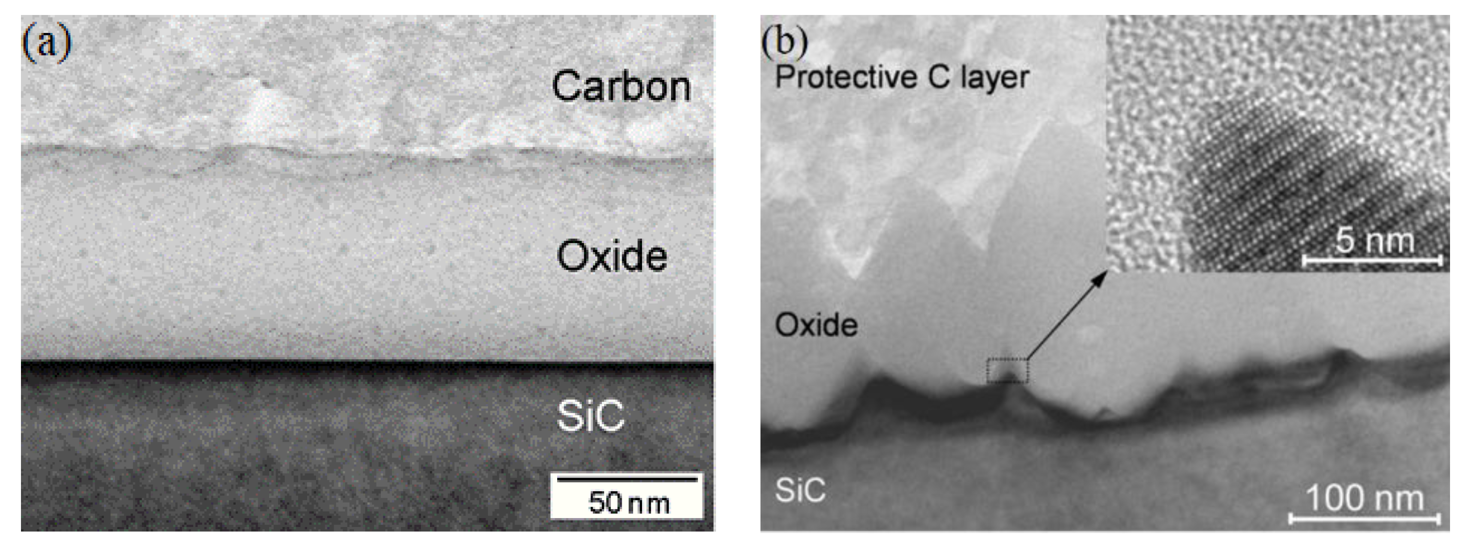
- The mechanism of CMP, PCMP, PAP, and ECMP was that the surface of single-crystal SiC was modified into a lower-hardness oxide layer (SiO2 and silicon oxycarbide) compared with the substrate, which was mechanically removed by the soft abrasive particles. CARE is a polishing technique that uses a metal catalyst to accelerate the chemical dissolution of single-crystal SiC in the absence of abrasive conditions, while the metal is used as a polishing disc to smooth-polish single-crystal SiC.
- (2)
- In the oxide layer, SiO2 was located at the top layer, and silicon oxycarbide, whose hardness was greater than that of SiO2 and less than that of SiC, was located at the interface between the oxide layer and SiC.
- (3)
- The MRR and surface quality were a coupled result of the surface oxidation and mechanical removal of single-crystal SiC. The balance between the oxide layer’s mechanical removal rate and the formation rate was necessary to obtain a smooth surface without defects.
- (4)
- The surface roughness after PAP and CARE was the smallest, while the MRR of ECMP was the highest. CMP is still the common precision polishing technology for single-crystal SiC in industrial production with comprehensive consideration of the experimental setup, the MRR, and the surface roughness.
- (5)
- Ultrasonic-assisted electrolyte plasma polishing of single-crystal SiC may be the future research direction that can be an effective way to greatly improve the MRR and surface quality.
Author Contributions
Funding
Conflicts of Interest
References
- Madar, R. Silicon carbide in contention. Nature 2004, 430, 974–975. [Google Scholar] [CrossRef] [PubMed]
- Dzurak, A. Diamond and silicon converge. Nature 2011, 479, 47–48. [Google Scholar] [CrossRef]
- Reis, F.; Li, G.; Dudy, L.; Bauernfeind, M.; Glass, S.; Hanke, W.; Thomale, R.; Schäfer, J.; Claessen, R. Bismuthene on a SiC substrate: A candidate for a high-temperature quantum spin Hall material. Science 2017, 357, 287–290. [Google Scholar] [CrossRef] [Green Version]
- Ruddy, F.H.; Seidel, J.G.; Haoqian, C.; Dulloo, A.R.; Sei-Hyung, R. High-resolution alpha-particle spectrometry using 4H silicon carbide semiconductor detectors. IEEE Trans. Nucl. Sci. 2006, 53, 1713–1718. [Google Scholar] [CrossRef]
- Puglisi, D.; Bertuccio, G. Silicon Carbide Microstrip Radiation Detectors. Micromachines 2019, 10, 835. [Google Scholar] [CrossRef] [Green Version]
- Kleppinger, J.W.; Chaudhuri, S.K.; Karadavut, O.; Mandal, K.C. Defect characterization and charge transport measurements in high-resolution Ni/n-4H-SiC Schottky barrier radiation detectors fabricated on 250 μm epitaxial layers. J. Appl. Phys. 2021, 129, 244501. [Google Scholar] [CrossRef]
- Chaudhuri, S.K.; Mandal, K.C. Radiation detection using n-type 4H-SiC Epitaxial Layer Surface Barrier Detectors. In Advanced Materials for Radiation Detection; Spring: Berlin/Heidelberg, Germany, 2021; pp. 183–209. [Google Scholar]
- Ohmi, T.; Miyashita, M.; Itano, M.; Imaoka, T.; Kawanabe, I. Dependence of thin-Oxide films quality on surface microroughness. IEEE Trans. Electron Devices 1922, 39, 537–545. [Google Scholar] [CrossRef]
- Grim, J.R.; Benamara, M.; Skowronski, M.; Everson, W.J.; Heydemann, V.D. Transmission electron microscopy analysis of mechanical polishing-related damage in silicon carbide wafers. Semicond. Sci. Technol. 2006, 21, 1709–1713. [Google Scholar] [CrossRef]
- Guoshun, P.; Yan, Z.; Guihai, L.; Xiaolei, S.; Chunli, Z.; Hua, G. Chemical mechanical polishing (CMP) of on-axis Si-face 6H-SiC wafer for obtaining atomically flat defect-free surface. J. Mater. Sci. Mater. Electron. 2013, 24, 5040–5047. [Google Scholar] [CrossRef]
- Guomei, C.; Zifeng, N.; Yawen, B.; Qingzhong, L.; Yongwu, Z. The role of interactions between abrasive particles and the substrate surface in chemical-mechanical planarization of Si-face 6H-SiC. RSC Adv. 2017, 7, 16938–16952. [Google Scholar] [CrossRef] [Green Version]
- Yamamura, K.; Takiguchi, T.; Ueda, M.; Hattori, A.N.; Zettsu, N. High-Integrity Finishing of 4H-SiC (0001) by Plasma-Assisted Polishing. Adv. Mater. Res. 2010, 126–128, 423–428. [Google Scholar] [CrossRef] [Green Version]
- Jia, G.; Li, B.; Zhang, J. Influence of SiC surface defects on materials removal in atmospheric pressure plasma polishing. Comput. Mater. Sci. 2018, 146, 26–35. [Google Scholar] [CrossRef]
- Zewei, Y.; Yan, H.; Xingwei, S.; Quan, W. UV-TiO2 photocatalysis-assisted chemical mechanical polishing 4H-SiC wafer. Mater. Manuf. Processes 2017, 33, 1214–1222. [Google Scholar] [CrossRef]
- Deng, H.; Hosoya, K.; Imanishi, Y.; Endo, K.; Yamamura, K. Electro-chemical mechanical polishing of single-crystal SiC using CeO2 slurry. Electrochem. Commun. 2015, 52, 5–8. [Google Scholar] [CrossRef] [Green Version]
- Yang, X.; Yang, X.; Kawai, K.; Arima, K.; Yamamura, K. Highly efficient planarization of sliced 4H–SiC (0001) wafer by slurryless electrochemical mechanical polishing. Int. J. Mach. Tools Manuf. 2019, 144, 103431. [Google Scholar] [CrossRef]
- Hara, H.; Sano, Y.; Mimura, H.; Arima, K.; Kubota, A.; Yagi, K.; Murata, J.; Yamauch, K. Novel abrasive-free planarization of 4H—SiC (0001) using catalyst. J. Electron. Mater. 2006, 35, L11–L14. [Google Scholar] [CrossRef]
- Kenta, A.; Hideyuki, H.; Junji, M.; Takeshi, I.; Ryota, O.; Keita, Y.; Yasuhisa, S.; Hidekazu, M.; Kazuto, Y. Atomic-scale flattening of SiC surfaces by electroless chemical etching in HF solution with Pt catalyst. Appl. Phys. Lett. 2007, 90, 202106. [Google Scholar] [CrossRef]
- van Dorp, D.H.; Sattler, J.J.H.B.; den Otter, J.H.; Kelly, J.J. Electrochemistry of anodic etching of 4H and 6H–SiC in fluoride solution of pH 3. Electrochim. Acta 2009, 54, 6269–6275. [Google Scholar] [CrossRef]
- Luo, H.; Ajmal, K.M.; Liu, W.; Yamamura, K.; Deng, H. Polishing and planarization of single crystal diamonds: State-of-the-art and perspectives. Int. J. Extrem. Manuf. 2021, 3, 022003. [Google Scholar] [CrossRef]
- Luo, Q.F.; Lu, J.; Xu, X.P. A comparative study on the material removal mechanisms of 6H-SiC polished by semi-fixed and fixed diamond abrasive tools. Wear 2016, 350–351, 99–106. [Google Scholar] [CrossRef]
- Zhou, L.; Audurier, V.; Pirouz, P.; Powell, J.A. Chemomechanical Polishing of Silicon Carbide. J. Electrochem. Soc. 1997, 144, L161–L163. [Google Scholar] [CrossRef]
- Guomei, C.; Zifeng, N.; Laijun, X.; Qingzhong, L.; Yongwu, Z. Performance of colloidal silica and ceria based slurries on CMP of Si-face 6H-SiC substrates. Appl. Surf. Sci. 2015, 359, 664–668. [Google Scholar] [CrossRef]
- Neslen, C.L.; Mitchel, W.C.; Hengehold, R.L. Effects of process parameter variations on the removal rate in chemical mechanical polishing of 4H-SiC. J. Electron. Mater. 2001, 30, 1271–1275. [Google Scholar] [CrossRef]
- Lee, H.S.; Jeong, H.D. Chemical and mechanical balance in polishing of electronic materials for defect-free surfaces. CIRP Ann. Manuf. Technol. 2009, 58, 485–490. [Google Scholar] [CrossRef]
- Lee, H.S.; Kim, D.I.; An, J.H.; Lee, H.J.; Kim, K.H.; Jeong, H. Hybrid polishing mechanism of single crystal SiC using mixed abrasive slurry (MAS). CIRP Ann. Manuf. Technol. 2010, 59, 333–336. [Google Scholar] [CrossRef]
- Heydemann, V.D.; Everson, W.J.; Gamble, R.D.; Snyder, D.; Skowronski, M. Chemi-mechanical polishing of on-Axis semi-insulating SiC substrates. Mater. Sci. Forum 2004, 457–460, 805–808. [Google Scholar] [CrossRef]
- Ho, A.J.; Sub, L.G.; Jae, L.W.; Chul, S.B.; Doo, S.J.; Ryeol, K.K.; Seo, H.D.; Jeong, H.D. Effect of Process Parameters on Material Removal Rate in Chemical Mechanical Polishing of 6H-SiC(0001). Mater. Sci. Forum 2008, 600–603, 831–834. [Google Scholar] [CrossRef]
- Yan, Z.; Guoshun, P.; Xiaolei, S.; Li, X.; Chunli, Z.; Hua, G.; Guihai, L. XPS, UV–vis spectroscopy and AFM studies on removal mechanisms of Si-face SiC wafer chemical mechanical polishing (CMP). Appl. Surf. Sci. 2014, 316, 643–648. [Google Scholar] [CrossRef]
- Hoshino, T.; Kurata, Y.; Terasaki, Y.; Susa, K. Mechanism of polishing of SiO2 films by CeO2 particles. J. Non Cryst. Solids 2001, 283, 129–136. [Google Scholar] [CrossRef]
- Tsai, M.Y.; Wang, S.M.; Tsai, C.C.; Yeh, T.S. Investigation of increased removal rate during polishing of single-crystal silicon carbide. Int. J. Adv. Manuf. Technol. 2015, 80, 1511–1520. [Google Scholar] [CrossRef]
- Hu, C.Y.; Lo, S.L.; Li, C.M.; Kuan, W.H. Treating chemical mechanical polishing (CMP) wastewater by electro-coagulation-flotation process with surfactant. J. Hazard Mater 2005, 120, 15–20. [Google Scholar] [CrossRef] [PubMed]
- Chou, W.L.; Wang, C.T.; Chang, W.C.; Chang, S.Y. Adsorption treatment of oxide chemical mechanical polishing wastewater from a semiconductor manufacturing plant by electrocoagulation. J. Hazard Mater 2010, 180, 217–224. [Google Scholar] [CrossRef] [PubMed]
- Ishikawa, Y.; Matsumoto, Y.; Nishida, Y.; Taniguchi, S.; Watanabe‡, J. Surface treatment of silicon carbide using TiO2(IV) photocatalyst. J. Am. Chem. Soc. 2003, 125, 6558–6562. [Google Scholar] [CrossRef] [PubMed]
- Osamu, O.; Toshiro, D.; Syuhei, K.; Tsutomu, Y.; Michio, U.; Tao, Y.; Isamu, K.; Koichiro, I.; Hideo, A. Effects of atmosphere and ultraviolet light irradiation on chemical mechanical polishing characteristics of SiC wafers. Jpn. J. Appl. Phys. 2012, 51, 05EF05. [Google Scholar] [CrossRef]
- Jing, L.; Yaguang, W.; Qiufa, L.; Xipeng, X. Photocatalysis assisting the mechanical polishing of a single-crystal SiC wafer utilizing an anatase TiO2 -coated diamond abrasive. Precis. Eng. 2017, 49, 235–242. [Google Scholar] [CrossRef]
- Yamamura, K.; Takiguchi, T.; Ueda, M.; Deng, H.; Hattori, A.N.; Zettsu, N. Plasma assisted polishing of single crystal SiC for obtaining atomically flat strain-free surface. CIRP Ann. Manuf. Technol. 2011, 60, 571–574. [Google Scholar] [CrossRef]
- Deng, H.; Takiguchi, T.; Ueda, M.; Hattori, A.N.; Zettsu, N.; Yamamura, K. Damage-free dry polishing of 4H-SiC combined with atmospheric-pressure water vapor plasma oxidation. Jpn. J. Appl. Phys. 2011, 50, 08JG05. [Google Scholar] [CrossRef]
- Deng, H.; Ueda, M.; Yamamura, K. Characterization of 4H-SiC (0001) surface processed by plasma-assisted polishing. Int. J. Adv. Manuf. Technol. 2012, 72, 1–7. [Google Scholar] [CrossRef]
- Deng, H.; Yamamura, K. XPS analysis of 4H-SiC surfaces oxidized by helium-based atmospheric-pressure water vapor plasma for plasma-assisted polishing. Mater. Sci. Forum 2013, 740–742, 514–517. [Google Scholar] [CrossRef]
- Deng, H.; Yamamura, K. Atomic-scale flattening mechanism of 4H-SiC (0 0 0 1) in plasma assisted polishing. CIRP Ann. Manuf. Technol. 2013, 62, 575–578. [Google Scholar] [CrossRef]
- Deng, H.; Endo, K.; Yamamura, K. Experimental Studies on Water Vapor Plasma Oxidation and Thermal Oxidation of 4H-SiC (0001) for Clarification of the Atomic-Scale Flattening Mechanism in Plasma Assisted Polishing. Mater. Sci. Forum 2014, 778–780, 587–590. [Google Scholar] [CrossRef]
- Deng, H.; Endo, K.; Yamamura, K. Comparison of thermal oxidation and plasma oxidation of 4H-SiC (0001) for surface flattening. Appl. Phys. Lett. 2014, 104, 101608. [Google Scholar] [CrossRef]
- Deng, H.; Endo, K.; Yamamura, K. Damage-free and atomically-flat finishing of single crystal SiC by combination of oxidation and soft abrasive polishing. Procedia CIRP 2014, 13, 203–207. [Google Scholar] [CrossRef] [Green Version]
- Deng, H.; Monna, K.; Tabata, T.; Endo, K.; Yamamura, K. Optimization of the plasma oxidation and abrasive polishing processes in Plasma assisted polishing for highly effective planarization of 4H-SiC. CIRP Ann. Manuf. Technol. 2014, 36, 529–532. [Google Scholar] [CrossRef] [Green Version]
- Deng, H.; Endo, K.; Yamamura, K. Competition between surface modification and abrasive polishing: A method of controlling the surface atomic structure of 4H-SiC (0001). Sci. Rep. 2015, 5, 1–6. [Google Scholar] [CrossRef] [Green Version]
- Li, C.; Bhat, I.B.; Wang, R.; Seiler, J. Electro-chemical mechanical polishing of silicon carbide. J. Electron. Mater. 2004, 33, 481–486. [Google Scholar] [CrossRef]
- Yamamura, K.; Hosoya, K.; Imanishi, Y.; Deng, H.; Endo, K. Preliminary study on highly efficient polishing of 4H-SiC by utilization of anodic oxidation. Adv. Mater. Res. 2014, 1017, 509–514. [Google Scholar] [CrossRef]
- Murata, J.; Yodogawa, K.; Ban, K. Polishing-pad-free electrochemical mechanical polishing of single-crystalline SiC surfaces using polyurethane–CeO2 core–shell particles. Int. J. Mach. Tools Manuf. 2017, 114, 1–7. [Google Scholar] [CrossRef]
- Gao, B.; Zhai, W.J.; Zhai, Q.; Xia, Y.L.; Wang, C.; Peng, K.X. Electro-chemical mechanical polishing of 4H-SiC for scratch-free surfaces with less oxide layer at high efficiency. ECS J. Solid State Sci. Technol. 2019, 8, P677–P684. [Google Scholar] [CrossRef]
- Yang, X.; Yang, X.; Sun, R.; Kawai, K.; Arima, K.; Yamamura, K. Obtaining atomically smooth 4H–SiC (0001) surface by controlling balance between anodizing and polishing in electrochemical mechanical polishing. Nanomanuf. Metrol. 2019, 2, 140–147. [Google Scholar] [CrossRef]
- Yang, X.; Sun, R.; Kawai, K.; Arima, K.; Yamamura, K. Surface modification and microstructuring of 4H-SiC(0001) by anodic oxidation with sodium chloride aqueous solution. ACS Appl. Mater. Interfaces 2019, 11, 2535–2542. [Google Scholar] [CrossRef]
- Murata, J.; Nagatomo, D. Investigation of electrolytic condition on abrasive-free electrochemical mechanical polishing of 4H-SiC using Ce thin film. ECS J. Solid State Sci. Technol. 2020, 9, 034002. [Google Scholar] [CrossRef]
- Deng, H.; Liu, N.; Endo, K.; Yamamura, K. Atomic-scale finishing of carbon face of single crystal SiC by combination of thermal oxidation pretreatment and slurry polishing. Appl. Surf. Sci. 2018, 434, 40–48. [Google Scholar] [CrossRef]
- Liu, N.; Yi, R.; Deng, H. Study of initiation and development of local oxidation phenomena during anodizing of SiC. Electrochem. Commun. 2018, 89, 27–31. [Google Scholar] [CrossRef]
- Yang, X.; Ohkubo, Y.; Endo, K.; Yamamura, K. AFM observation of initial oxidation stage of 4H-SiC (0001) in electrochemical mechanical polishing. Procedia CIRP 2018, 68, 735–740. [Google Scholar] [CrossRef]
- Yang, X.; Sun, R.; Ohkubo, Y.; Kawai, K.; Arima, K.; Endo, K.; Yamamura, K. Investigation of anodic oxidation mechanism of 4H-SiC (0001) for electrochemical mechanical polishing. Electrochim. Acta 2018, 271, 666–676. [Google Scholar] [CrossRef]
- Okamoto, T.; Sano, Y.; Tachibana, K.; Pho, B.V.; Arima, K.; Inagaki, K.; Yagi, K.; Murata, J.; Sadakuni, S.; Asano, H.; et al. Improvement of Removal Rate in Abrasive-Free Planarization of 4H-SiC Substrates Using Catalytic Platinum and Hydrofluoric Acid. Jpn. J. Appl. Phys. 2012, 51, 046501. [Google Scholar] [CrossRef]
- Sano, Y.; Arima, K.; Yamauchi, K. Planarization of SiC and GaN Wafers Using Polishing Technique Utilizing Catalyst Surface Reaction. ECS J. Solid State Sci. Technol. 2013, 2, N3028–N3035. [Google Scholar] [CrossRef]
- Lsohashi, A.; Sano, Y.; Okamoto, T.; Tachibana, K.; Arima, K.; Lnagaki, K.; Yagi, K.; Sadakuni, S.; Morikawa, Y.; Yamauchi, K. Study on Reactive Species in Catalyst-Referred Etching of 4H–SiC using Platinum and Hydrofluoric Acid. Mater. Sci. Forum 2013, 740–742, 847–850. [Google Scholar] [CrossRef]
- Yagi, K.; Murata, J.; Kubota, A.; Sano, Y.; Hara, H.; Okamoto, T.; Arima, K.; Mimura, H.; Yamauchi, K. Catalyst-referred etching of 4H-SiC substrate utilizing hydroxyl radicals generated from hydrogen peroxide molecules. Surf. Interface Anal. 2008, 40, 998–1001. [Google Scholar] [CrossRef]
- Kubota, A.; Yagi, K.; Murata, J.; Yasui, H.; Miyamoto, S.; Hara, H.; Sano, Y.; Yamauchi, K. A Study on a Surface Preparation Method for Single-Crystal SiC Using an Fe Catalyst. J. Electron. Mater. 2008, 38, 159–163. [Google Scholar] [CrossRef]
- Isohashi, A.; Bui, P.V.; Toh, D.; Matsuyama, S.; Sano, Y.; Inagaki, K.; Morikawa, Y.; Yamauchi, K. Chemical etching of silicon carbide in pure water by using platinum catalyst. Appl. Phys. Lett. 2017, 110, 201601. [Google Scholar] [CrossRef] [Green Version]
- Van Bui, P.; Toh, D.; Isohashi, A.; Matsuyama, S.; Inagaki, K.; Sano, Y.; Yamauchi, K.; Morikawa, Y. Platinum-catalyzed hydrolysis etching of SiC in water: A density functional theory study. Jpn. J. Appl. Phys. 2018, 57, 055703. [Google Scholar] [CrossRef]
- Okamoto, T.; Sano, Y.; Hara, H.; Hatayama, T.; Arima, K.; Yagi, K.; Murata, J.; Sadakuni, S.; Tachibana, K.; Shirasawa, Y.; et al. Reduction of Surface Roughness of 4H-SiC by Catalyst-Referred Etching. Mater. Sci. Forum 2010, 645–648, 775–778. [Google Scholar] [CrossRef]
- Yan, Z.; Guoshun, P.; Xiaolei, S.; Hua, G.; Guihai, L.; Zhonghua, G. Chemical mechanical planarization (CMP) of on-axis Si-face SiC wafer using catalyst nanoparticles in slurry. Surf. Coat. Technol. 2014, 251, 48–55. [Google Scholar] [CrossRef]
- Zhao, Q.; Sun, Z.; Guo, B. Material removal mechanism in ultrasonic vibration assisted polishing of micro cylindrical surface on SiC. Int. J. Mach. Tools Manuf. 2016, 103, 28–39. [Google Scholar] [CrossRef]
- Hu, Y.; Shi, D.; Hu, Y.; Zhao, H.; Sun, X. Investigation on the material removal and surface generation of a single crystal SiC wafer by ultrasonic chemical mechanical polishing combined with ultrasonic lapping. Materials 2018, 11, 2022. [Google Scholar] [CrossRef] [PubMed] [Green Version]
- Yang, X.; Yang, X.; Kawai, K.; Arima, K.; Yamamura, K. Ultrasonic-assisted anodic oxidation of 4H-SiC (0001) surface. Electrochem. Commun. 2019, 100, 1–5. [Google Scholar] [CrossRef]
- Ashokkumar, M.; Sunartio, D.; Kentish, S.; Mawson, R.; Simons, L.; Vilkhu, K.; Versteeg, C. Modification of food ingredients by ultrasound to improve functionality: A preliminary study on a model system. Innov. Food Sci. Emerg. Technol. 2008, 9, 155–160. [Google Scholar] [CrossRef]
- Makino, K.; Mossoba, M.M.; Riesz, P. Chemical effects of ultrasound on aqueous solutions. Formation of hydroxyl radicals and hydrogen atoms. J. Phys. Chem. 1983, 87, 1369–1377. [Google Scholar] [CrossRef]
- Han, W.; Fang, F. Fundamental aspects and recent developments in electropolishing. Int. J. Mach. Tools Manuf. 2019, 139, 1–23. [Google Scholar] [CrossRef]
- Nestler, K.; Böttger-Hiller, F.; Adamitzki, W.; Glowa, G.; Zeidler, H.; Schubert, A. Plasma electrolytic polishing—An Overview of applied technologies and current challenges to extend the polishable material range. Procedia CIRP 2016, 42, 503–507. [Google Scholar] [CrossRef]
- Danilov, I.; Hackert-Oschatzchen, M.; Zinecker, M.; Meichsner, G.; Edelmann, J.; Schubert, A. Process understanding of plasma electrolytic polishing through multiphysics simulation and inline metrology. Micromachines 2019, 10, 214. [Google Scholar] [CrossRef] [PubMed] [Green Version]
- Kellogg, H.H. Anode Effect in Aqueous Electrolysis. J. Electrochem. Soc. 1950, 97, 133–142. [Google Scholar] [CrossRef]
- Kalenchukova, V.O.; Nagula, P.K.; Tretinnikov, D.L. About changes in the chemical composition of the electrolyte in the process of electrolytic-plasma treatment of materials. Mater. Methods Technol. 2015, 9, 404–413. [Google Scholar]
- Vana, D.; Podhorsky, S.; Hurajt, M.; Hanzen, V. Surface Properties of the Stainless Steel X10 CrNi 18/10 after Aplication of Plasma Polishing in Electrolyte. Int. J. Mod. Eng. Res. 2013, 3, 788–792. [Google Scholar]
- Wang, J.; Suo, L.C.; Guan, L.L.; Fu, Y.L. Analytical study on mechanism of electrolysis and plasma polishing. Adv. Mater. Res. 2012, 472–475, 350–353. [Google Scholar] [CrossRef]
- Cornelsen, M.; Deutsch, C.; Seitz, H. Electrolytic plasma polishing of pipe inner surfaces. Metals 2018, 8, 12. [Google Scholar] [CrossRef] [Green Version]
- Clements, J.S.; Sato, M.; Davis, R.H. Preliminary Investigation of Prebreakdown Phenomena and Chemical Reactions Using a Pulsed High-Voltage Discharge in Water. IEEE Trans. Ind. Appl. 1987, 24, 224–235. [Google Scholar] [CrossRef]
- Sun, B.; Kunitomo, S.; Igarashi, C. Characteristics of ultraviolet light and radicals formed by pulsed discharge in water. J. Phys. D Appl. Phys. 2006, 39, 3814–3820. [Google Scholar] [CrossRef]
- Parfenov, E.V.; Farrakhov, R.G.; Mukaeva, V.R.; Gusarov, A.V.; Nevyantseva, R.R.; Yerokhin, A. Electric field effect on surface layer removal during electrolytic plasma polishing. Surf. Coat. Technol. 2016, 307, 1329–1340. [Google Scholar] [CrossRef]
- Zeidler, H.; Boettger-Hiller, F.; Edelmann, J.; Schubert, A. Surface finish machining of medical parts using plasma electrolytic polishing. Procedia CIRP 2016, 49, 83–87. [Google Scholar] [CrossRef]
- Ablyaz, T.R.; Muratov, K.R.; Ushomirskaya, L.A.; Zarubin, D.A.; Sidhu, S.S. Electrolytic plasma polishing technique for improved surface finish of ED machined components. Eng. Solid Mech. 2019, 7, 131–136. [Google Scholar] [CrossRef]
- Valiev, R.I.; Khafizov, A.A.; Shakirov, Y.I.; Sushchikova, A.N. Polishing and deburring of machine parts in plasma of glow discharge between solid and liquid electrodes. IOP Conf. Ser. Mater. Sci. Eng. 2015, 86, 012026. [Google Scholar] [CrossRef]
- Cornelsen, M.; Deutsch, C.; Seitz, H. Influence of the Velocity and the Number of Polishing Passages on the Roughness of Electrolytic Plasma Polished Pipe Inner Surfaces. Metals 2018, 8, 330. [Google Scholar] [CrossRef] [Green Version]
- Kusmanov, S.; Zhirov, A.; Kusmanova, I.; Belkin, P. Aspects of anodic plasma electrolytic polishing of nitrided steel. Surf. Eng. 2017, 35, 507–511. [Google Scholar] [CrossRef]
- Li, S.; Wu, Y.; Yamamura, K.; Nomura, M.; Fujii, T. Improving the grindability of titanium alloy Ti–6Al–4V with the assistance of ultrasonic vibration and plasma electrolytic oxidation. CIRP Ann. Manuf. Technol. 2017, 66, 345–348. [Google Scholar] [CrossRef]
- Ma, G.; Li, S.; Liu, X.; Yin, X.; Jia, Z.; Liu, F. Combination of Plasma Electrolytic Processing and Mechanical Polishing for Single-Crystal 4H-SiC. Micromachines 2021, 12, 606. [Google Scholar] [CrossRef] [PubMed]
- Yin, X.; Li, S.; Ma, G.; Jia, Z.; Liu, X. Investigation of oxidation mechanism of SiC single crystal for plasma electrochemical oxidation. RSC Adv. 2021, 11, 27338–27345. [Google Scholar] [CrossRef]


| No. | Photocatalysis | UV | Electron Capturer | pH | Abrasive | Dispersant |
|---|---|---|---|---|---|---|
| 1# | TiO2 | UV | H2O2 | 2 | SiO2 | (NaPO3)6 |
| 2# | TiO2 | - | H2O2 | 2 | SiO2 | (NaPO3)6 |
| 3# | TiO2 | UV | K2FeO4 | 2 | SiO2 | (NaPO3)6 |
| 4# | TiO2 | UV | H2O2 | 13 | SiO2 | (NaPO3)6 |
| 5# | TiO2 | UV | - | 2 | SiO2 | (NaPO3)6 |
| Polishing Technologies | Ra (nm) | MRR (μm/h) | Remark | ||
|---|---|---|---|---|---|
| Max | Min | Max | Min | ||
| CMP | 0.52 [27] | 0.108 [28] | 1.3 [31] | 0.32 [26] | (a) |
| PCMP | 0.915 [36] | 0.35 [14] | 0.95 [14] | 0.115 [36] | |
| PAP | 0.2 [39] | 0.06 [38] | 0.185 [42] | 0.08 [40] | |
| ECMP | 0.51 [49] | 0.23 [15] | 3.62 [15] | 2.3 [53] | (b) |
| CARE | 0.1 [61] | 0.05 [66] | 0.5 [58] | 0.03 [62] | |
| Polishing Technologies | CMP | PCMP | PAP | ECMP | CARE |
|---|---|---|---|---|---|
| Mechanism | Chemical oxidation + abrasive polishing | Photocatalytic oxidation + abrasive polishing | Atmospheric plasma oxidation + abrasive polishing | Electrochemical oxidation + abrasive polishing | Chemical dissolution |
| MRR | Medium | Medium | Low | High | Low |
| Ra | Medium | Medium | Low | High | Low |
| Ecological level | Low | High | Medium | High | Low |
| Energy consumption | Low | Medium | High | High | Low |
| Controllability | High | Medium | Low | Low | Medium |
Publisher’s Note: MDPI stays neutral with regard to jurisdictional claims in published maps and institutional affiliations. |
© 2022 by the authors. Licensee MDPI, Basel, Switzerland. This article is an open access article distributed under the terms and conditions of the Creative Commons Attribution (CC BY) license (https://creativecommons.org/licenses/by/4.0/).
Share and Cite
Ma, G.; Li, S.; Liu, F.; Zhang, C.; Jia, Z.; Yin, X. A Review on Precision Polishing Technology of Single-Crystal SiC. Crystals 2022, 12, 101. https://doi.org/10.3390/cryst12010101
Ma G, Li S, Liu F, Zhang C, Jia Z, Yin X. A Review on Precision Polishing Technology of Single-Crystal SiC. Crystals. 2022; 12(1):101. https://doi.org/10.3390/cryst12010101
Chicago/Turabian StyleMa, Gaoling, Shujuan Li, Feilong Liu, Chen Zhang, Zhen Jia, and Xincheng Yin. 2022. "A Review on Precision Polishing Technology of Single-Crystal SiC" Crystals 12, no. 1: 101. https://doi.org/10.3390/cryst12010101