Review

Recent Developments in Flexible Transparent Electrode

1
State Key Laboratory of Luminescent Materials and Devices, Institute of Polymer Optoelectronic Materials and Devices, South China University of Technology, Guangzhou 510640, China
2
Guangxi Key Laboratory of Agricultural Resources Chemistry and Biotechnology, Yulin Normal University, Yulin 537000, China
3
Department of Intelligent Manufacturing, Wuyi University, Jiangmen 529020, China
4
State Key Laboratory of Advanced Materials and Electronic Components, Fenghua Electronic Industrial Park, No. 18 Fenghua Road, Zhaoqing 526020, China
5
School of Electrical Engineering & Intelligentization, Dongguan University of Technology, No. 1 Daxue Rd, Dongguan 523808, China
*
Authors to whom correspondence should be addressed.
Crystals 2021, 11(5), 511; https://doi.org/10.3390/cryst11050511
Submission received: 15 March 2021 / Revised: 20 April 2021 / Accepted: 26 April 2021 / Published: 5 May 2021
(This article belongs to the Special Issue Liquid Crystals in China)

Abstract

:
With the rapid development of flexible electronic devices (especially flexible LCD/OLED), flexible transparent electrodes (FTEs) with high light transmittance, high electrical conductivity, and excellent stretchability have attracted extensive attention from researchers and businesses. FTEs serve as an important part of display devices (touch screen and display), energy storage devices (solar cells and super capacitors), and wearable medical devices (electronic skin). In this paper, we review the recent progress in the field of FTEs, with special emphasis on metal materials, carbon-based materials, conductive polymers (CPs), and composite materials, which are good alternatives to the traditional commercial transparent electrode (i.e., indium tin oxide, ITO). With respect to production methods, this article provides a detailed discussion on the performance differences and practical applications of different materials. Furthermore, major challenges and future developments of FTEs are also discussed.

1. Introduction

With the development of science and technology, people have increasing requirements with respect to flexible electronic devices. Flexible transparent electrodes (FTEs) are essential components for flexible electronic equipment, such as LCD, OLED, and TFT. Hence, FTEs have attracted more and more attention, which has led to extensive research in recent years [1,2,3,4]. At present, the ITO electrode, acting as the representative transparent electrode, has been commercialized and extensively used due to its high transparency (≈85%) and low sheet resistance (100–500 Ω∙sq−1). Unfortunately, the production of ITO is hindered by the severe shortage of indium, high production cost, and the brittleness of the material itself [5]. At the same time, people have increasing requirements for the flexibility, stretchability, and foldability of flexible electronic devices. However, the preparation of ITO electrodes requires subsequent processes such as high-temperature annealing, which further limits its application and development. As it is difficult for ITO electrodes to be manufactured on flexible substrates which are not resistant to high temperature, finding alternative materials to ITO and meeting commercial requirements has become a research hotspot. These FTEs have excellent conductivity, optical transmittance, and mechanical properties, and they can be mass-produced. The FTEs reviewed in this article are made of different materials, including metal materials (metal nanowire, ultra-thin metal films, and metal mesh) [6,7], carbon-based materials (carbon nanotubes (CNTs) and graphene) [3,8], conducting polymers (CPs) [9], and composite materials [10,11]. These various electrode materials all have their own advantages, which make them good options for new-generation FTEs. Previous studies have demonstrated that these materials not only have excellent flexibility, but also have lower electrical resistivity and higher light transmittance than ITO electrode. This review comprehensively summarizes the preparation methods and performance of these electrode materials. High-performance FTEs have a wide range of applications in optoelectronic devices, such as touch screens [12], solar cells [13], super capacitors [14], flexible electroluminescent devices, and wearable devices [15]. Moreover, problems in the industry and future development directions are also outlined in this article, hoping to provide a reference for the design and manufacture of FTEs.

2. Electrode Materials

2.1. Metal

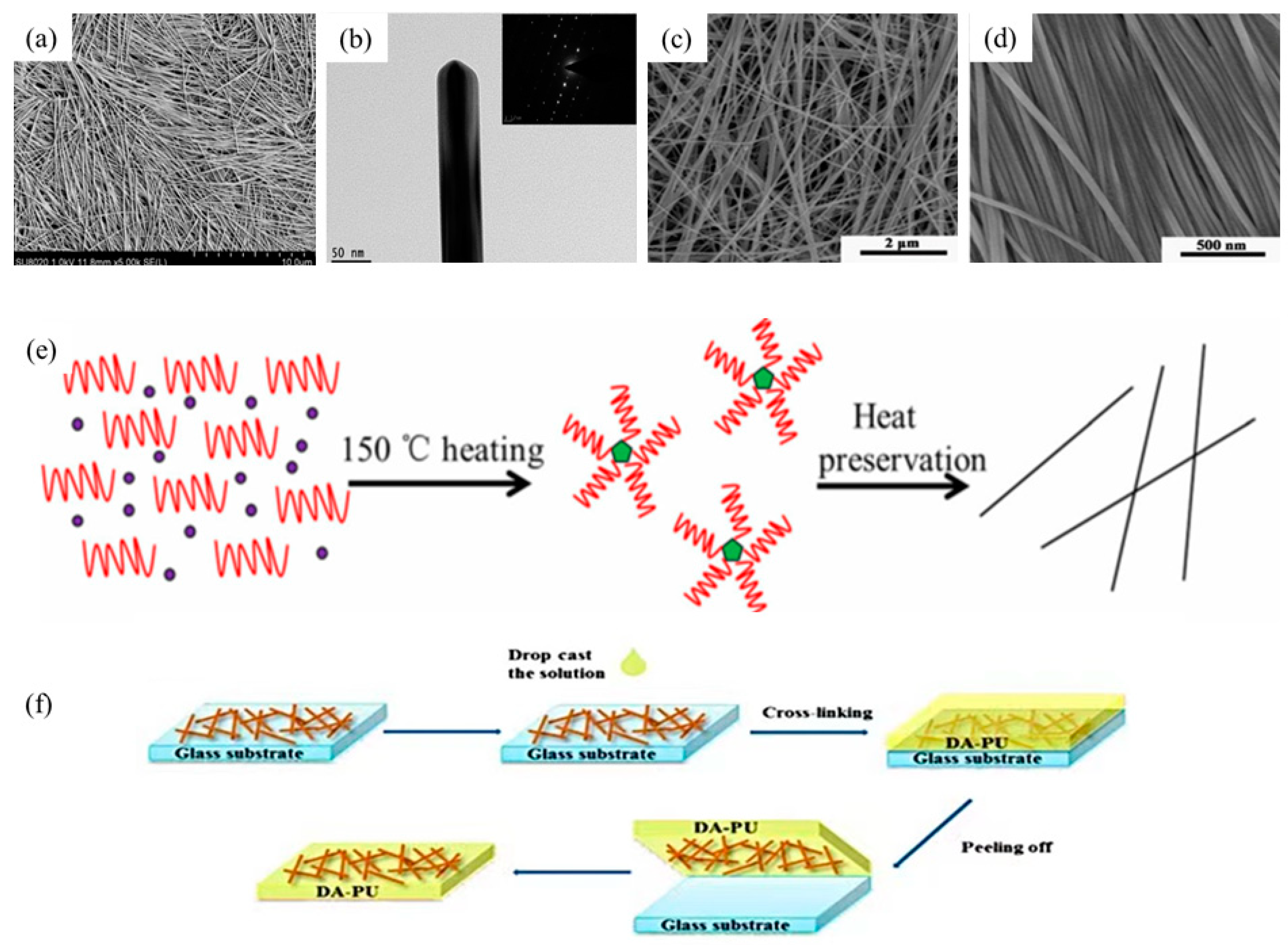
2.1.1. Metal Nanowires

Because of their excellent photoelectric properties, chemical properties, mechanical properties, and flexibility, metal nanowires have become the most likely substitute for ITO [16,17,18,19]. Noble metal nanowires such as gold and silver (Figure 1a,b) were rapidly developed and entered the market first [20]. The preparation methods include the liquid polyol method [21,22], template method (soft template method [23,24] and hard template method [25]), self-assembly method [26,27], ultrasonic reduction method [28], wet chemical method [29,30], and ultraviolet (UV) laser pattern method [31]. Among them, liquid polyols are currently the easiest method to achieve high-efficiency production owing to their high effect, simple production, and low cost, and a simple method for Ag nanowire (AgNW) synthesis is shown in Figure 1e. The template method can control the morphology and properties of the final product, which is easy to synthesize [16]. As for UV laser patterning, the light transmittance, haze, and conductivity of AgNWs can be changed by adjusting the laser power. At the same time, nanowires can be purified using the precipitation method [32,33] and heat treatment [34], which can improve the density and conductivity of the nanowires. Atkinson et al. found that the high transparency of AgNWs (94%) in the infrared region (wavelength is 2500 nm) is much higher than that of traditional ITO electrodes (35%). In addition, thinner AgNWs result in a larger diameter and higher transparency. This characteristic of AgNWs has a significant impact on the development of solar cells and window coatings [35]. Liu et al. successfully prepared AgNWs in a water environment by adjusting the appropriate pH value, and the aqueous phase environment enabled the samples to have better biological applications [36]. Previous studies improved the performance of AgNWs by coating them with transparent conducting oxide (TCO) layers (such as ITO and ZnO), but this process is complex with a high cost, and it results in brittleness of the FTEs. Yu et al. proposed a hot lamination process to solve the problems of poor electrical conductivity and adhesion of AgNWs, which greatly reduced the square resistance (from 100 to 12.5 Ω∙sq−1) under the condition of constant optical transmittance (94.5%) [37]. AgNWs electrodes are easily oxidized at high temperature, which increases their resistance. Photoresist encapsulation proved to be a superior method to improve the reliability of AgNWs electrodes under harsh conditions [38]. In addition, Pantoja et al. studied the performance (including reflectance, transmittance, emissivity, and haze) of AgNWs in the infrared spectrum and prepared low-emissivity AgNWs films, reducing the thermal emissivity of the substrates [39]. Copper is second only to silver in metal conductivity, with low cost and high yield. Therefore, Cu nanowires (CuNWs) were also rapidly developed in recent years; Figure 1f shows a schematic diagram of a healable nanocomposite conductor based on CuNWs, with a sheet resistance of 22.3 Ω·sq1 and 66.5% transmittance at a wavelength of 550 nm [40]. Huang et al. synthesized CuNWs (Figure 1c,d) with high purity, large aspect ratio, good dispersion, and controllable morphology using the hydrothermal method [41]. Moreover, Duong et al. innovated a simple, low-cost, and environmentally friendly method for preparing CuNW-based flexible electrodes using polyethylene-based inks. It was also verified that copper salt, capping agent, reducing agent, reaction temperature, and other conditions play an important role in controlling the morphology of CuNWs [42]. In order to further improve the conductivity of metal nanowires, the influence of various factors on the nanowires has been studied through mathematical modeling methods and verified through experiments [43,44,45]. It was found that orientation restriction can improve the unidirectional conductivity of metal nanowires, while randomness is beneficial to the conductivity of the metal network.

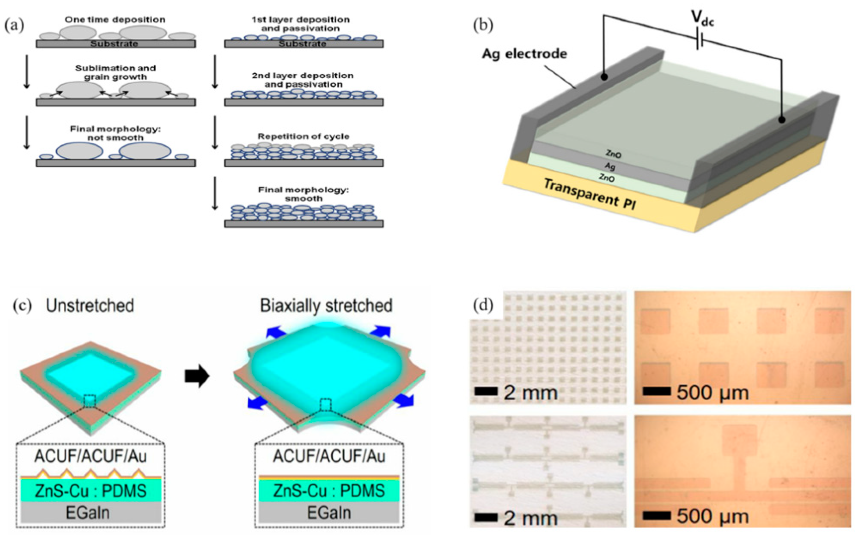
2.1.2. Ultra-Thin Metal Films
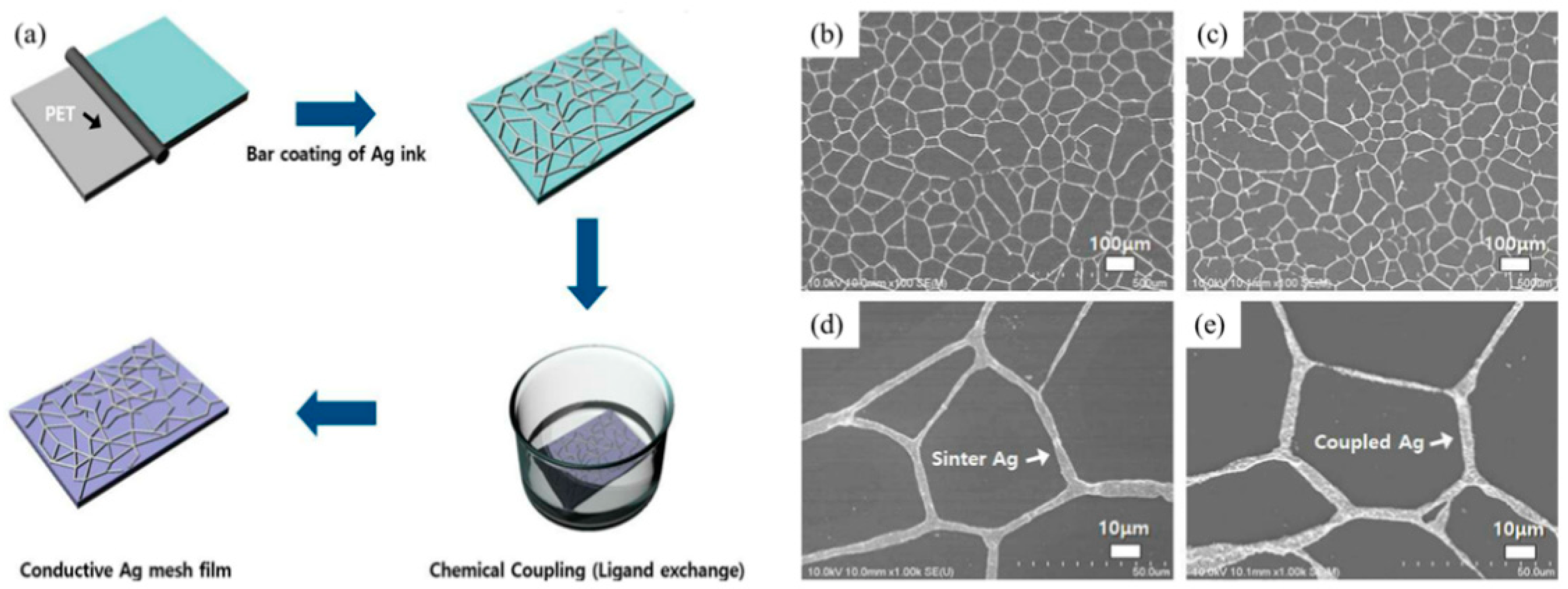
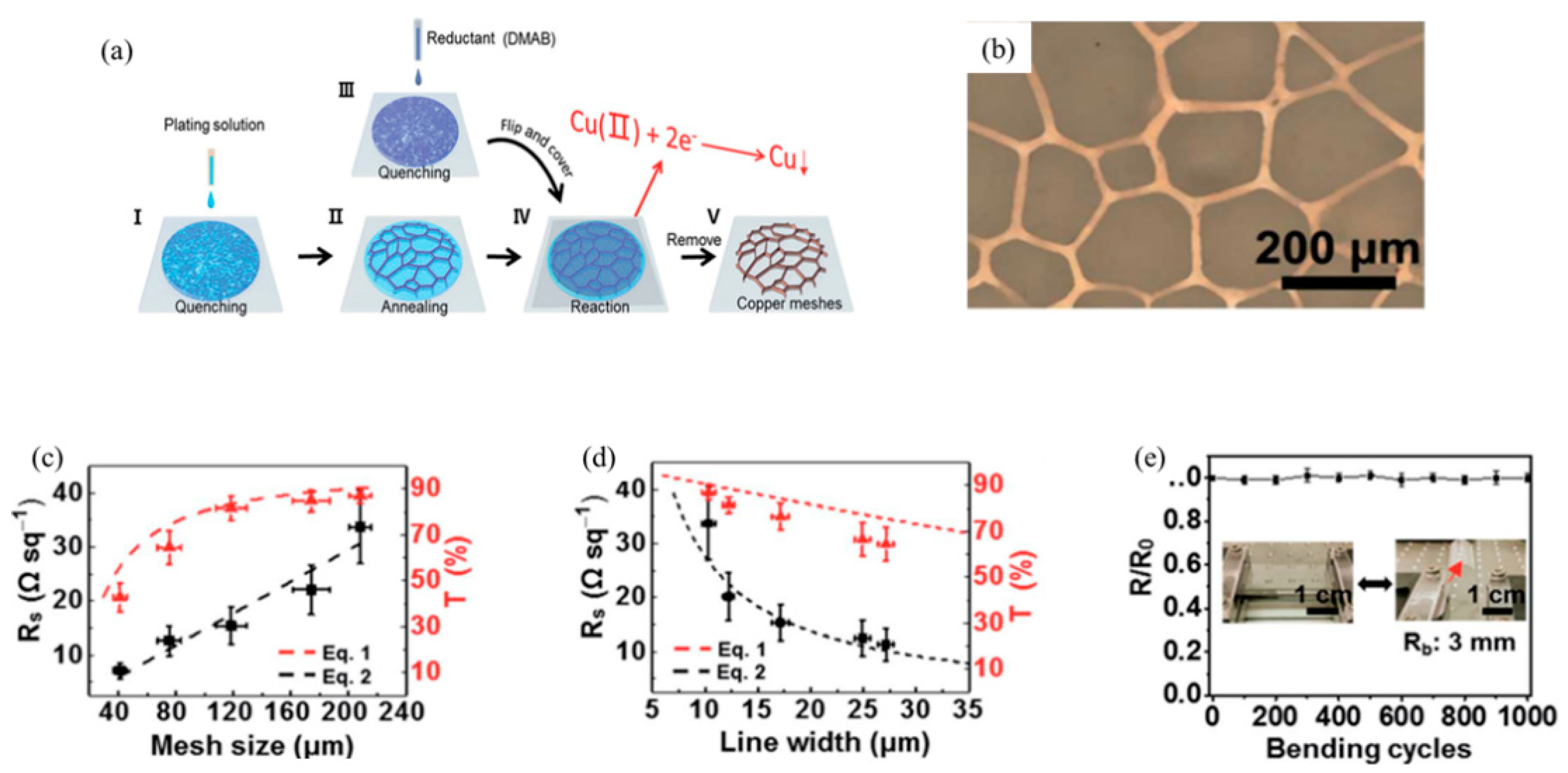
An ultra-thin metal film has the advantages of high stability, simple manufacturing process, and low cost [46,47]. Compared with metal nanowires, it has lower roughness and does not reduce the display resolution because of no scattering [48], which is conducive to display applications. However, because it must satisfy both high conductivity and optical transmittance, the film should be thin enough (<12 nm) [49]. Previous studies successfully prepared Au [11], Ag [50], Cu [51], Al [49], Cr [52], Ni [46], and other metal thin films. The preparation methods were mainly room-temperature sputtering deposition [48] and high-temperature thermal deposition [53]. The growth of a metal film on a substrate is generally divided into three stages (nucleation, coalescence, and thickness growth), and the performance of the film is affected by the various sputtering conditions. Results showed that silver clusters will form metal islands during the deposition process, making the film nonconductive [54]. This defect can be suppressed by multilayer deposition passivation, the process of which is shown in Figure 2a [55]. In addition, the introduction of a wetting layer can limit the migration and agglomeration of metal atoms under heating conditions to smoothen the film surface, as well as form defects, to increase the adhesion strength with the substrate. However, due to its high optical reflectivity rather than high absorptivity, the metal film has limited transmittance. It is well known that the optical transmittance of a metal film is extremely low. To deal with these problems, adding a dielectric antireflection layer to both sides of the metal layer is significant, resulting in an electrode structure known as the dielectric/metal/dielectric (DMD) structure [56,57]. However, in the DMD structure, Ag will migrate from the undisturbed region to the disturbed region with the passage of time, resulting in discontinuity of the Ag layer, thus, insulation of the electrode. One way to slow the loss of electrode life is to keep the substrate clean and pay attention to storage conditions [58]. Figure 2b shows a schematic structure of a ZnO/Ag/ZnO transparent heater, where the addition of 5% Ni could inhibit the diffusion of Ag atoms and effectively improve the thermal stability of Ag films [50]. Xie et al. investigated a low-resistance (7 Ω∙sq1) and high-transparency (73%) MoO3/Ag/WO3 top transparent electrode and successfully applied it to solar cells. Tuo et al. suggested replacing Ag in DMD structures with Cu, whereas adding a small amount of Ni (5%) to Cu could suppress the diffusion of Cu atoms. They also proved that WO3−x/Cu:Ni/WO3−x structures are fairly stable three-dimensional structures [59]. However, obviously, the highest conductivity and the best transmittance cannot be obtained at the same time. Surprisingly, it was confirmed that the fatigue strength of ultra-thin metal films is greater than that of thick films on account of the increase in yield stress and the formation of nano twins [60]. Furthermore, Cr and Ni films can maintain high optical transparency in the full wavelength range [61], while metal films such as Ag maintain high light transmittance only at specific wavelengths. In the ultra-thin gold–silver–gold multilayer film thermally deposited on flexible substrates by Bauch et al., the transmission spectrum was extended [53]. In addition, the stability of Ag thin films is poor. Studies have shown that metal doping is a good way to significantly improve the stability of Ag. In order to further improve the performance, Shi et al. deposited a micron silver grid on an Ni film, which reduced the resistivity from 390 Ω∙sq1 to 20 Ω∙sq−1 while keeping the transparency (78%) largely unchanged [46]. Afterward, Dong et al. fabricated high-performance Au film FTEs and used them to make a foldable perovskite light-emitting diode (PELED) and a biaxially stretchable alternating current electroluminescence (ACEL) display (Figure 2 c,d) [11]. Ji et al. proposed a flexible DMD-based electrode, with a relative optical transmittance higher than 100%. A thin metal film was sandwiched between two antireflective media to achieve high optical transparency and low fog, and it showed good compatibility with other substrates [48].

2.1.3. Metal Mesh

A metal mesh has good flexibility and mechanical properties; moreover, because of its three-dimensional (3D) shape, there is no strict limit on the thickness. Different combinations of transmittance and conductivity can be customized by adjusting line widths and spacing. The current preparation processes mainly include the heat treatment method [62], template method [63], lithography [64], imprinting [65], and laser pulse etching [66]. In order for them to be commercially available, it is necessary to find a high-throughput and low-cost preparation process. Moon et al. produced FTEs by flash sintering with a reverse-offset Ag screen pattern, and they experimentally proved that multi-pulse flash sintering could effectively reduce the sample temperature, increase the stability of the films, eliminate the damage or microstructure defects of the substrate, and achieve better performance (Rs = 27 Ω·sq−1 and transmittance = 84.7%) [67]. Kim et al. prepared silver grid films on flexible substrates through self-assembly and coupling processes (Figure 3), and they found that chemical coupling could effectively the improve conductivity (8.2 Ω·sq1) and light transmittance (>88%) with a figure of merit (FoM) value of 350 [68]. Li et al. proposed combining electroless plating with a recrystallized ice crystal template to prepare a flexible transparent copper mesh with controllable line width and mesh size (Figure 4) [69]. This method can also be applied to other metal meshes. In addition, Muzzillo et al. explored the principle of metal mesh fabrication using crack film lithography (CFL) and obtained controllable performance. This method has low cost, high speed, and high quality, and it can be widely applied to monolithically integrated thin-film photovoltaic (PV) modules [70]. However, a metal mesh cracks easily during use; thus, it was proven that it can be repaired by electrodeposition to further improve service life [71].

2.2. Carbon-Based Materials

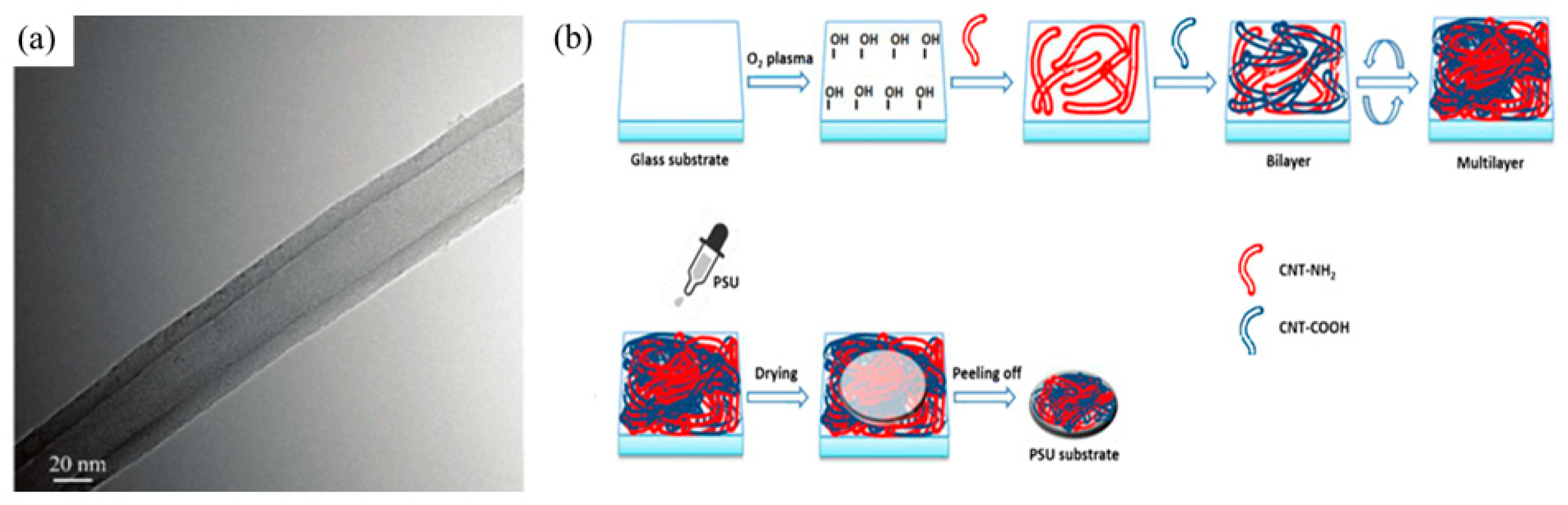
2.2.1. Carbon Nanotubes
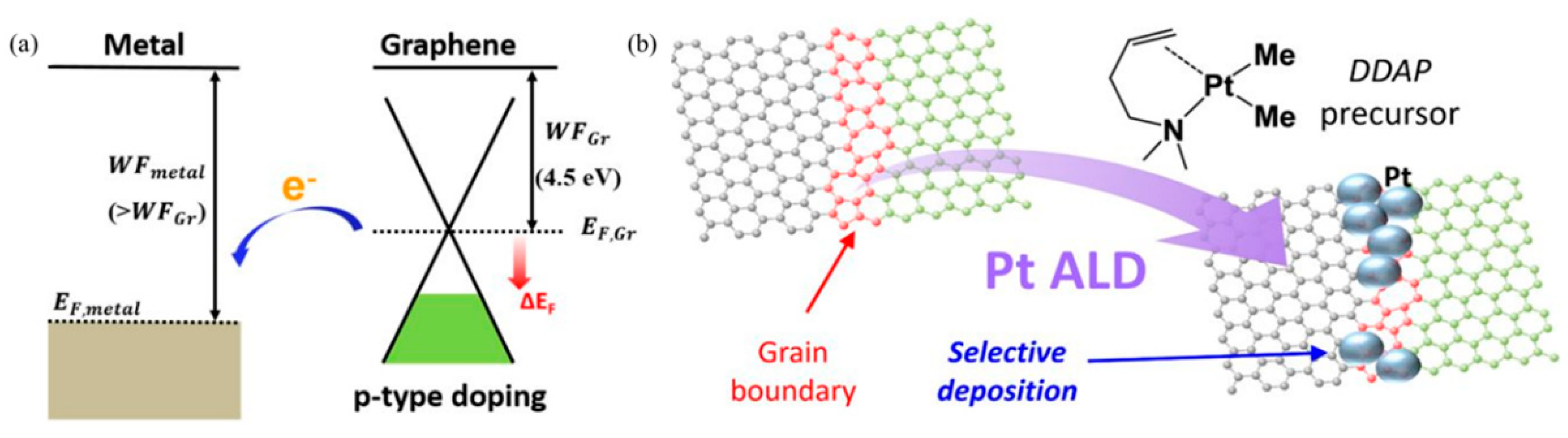
Carbon Nanotubes (CNTs) have attracted the attention of researchers because of their excellent mechanical properties, photoelectric properties, thermal stability, and large specific surface area, which has been studied for a long period; good reviews on CNTs have previously been published [72,73,74,75]. These excellent properties are related to the sp2 hybridization of carbon atoms [76]. CNTs can be categorized into multiwalled carbon nanotubes (NWCNTs) and single-walled carbon nanotubes (SWCNTs) [77], as well as armchair type, serrated type, and chiral type [68]. Figure 5a shows a TEM image of CNTs [73]. Currently, graphite is used as a raw material, whereby electrophoretic coating [78], ultrasonic spraying [79], dipping [80], brush coating [81], rod coating [82], and transfer printing [83] methods have been used to produce CNTs, and CNTs containing carbon impurities can be purified by annealing [84], chemical oxidation [85], and polymer introduction [86]. However, the abovementioned synthesis methods have the disadvantages of complicated postprocesses and large film roughness. Multilayer transfer printing (MTP) technology is a good alternative to the above synthesis methods [87]. Oytun et al. coated CNTs with positive and negative charges on the glass substrates by multilayer deposition; then, chemical and thermal post-treatment was carried out, before the electrode was transferred to the polymer film (Figure 5b). For 12-layer MWCNTs and SWCNTs, the maximum FoM is 2.52 × 10⁻⁶ Ω −1 at 68% light transmittance and 1.14 × 10⁻³ Ω −1 at 81% light transmittance [88]. In addition, atoms, molecules, polymers, metal nanoparticles, and cellulose can be used to modify the surface and ends of CNTs [72,89]; alternatively, they can be inserted into the hollow space of the nanotube [89]. Modification can further improve the conductivity and optical transmittance of CNTs. Sergey et al. thoroughly studied the mechanism of nitrogen-modified CNTs to increase electrical conductivity, and they determined that nitrogen has the highest binding energy in the graphite-like state [90]. Moreover, Awadallah et al. discovered a method of modifying CNTs with carbon nanoparticles, and they prepared hybrid carbon nano products with different properties and morphologies from the original CNTs [72]. It was also proven that the interaction between CNTs can increase the tensile strength of the electrodes [91]. Furthermore, the size of CNTs also has great influence on their properties. NWCNTs with a thinner diameter have higher transparency, whereas longer NWCNTs have higher conductivity [92]. In practical applications, thin-film transistors (TFT) were successfully prepared using CNTs [93].

2.2.2. Graphene

Among carbon-based materials, CNTs are one-dimensional (1D), while graphene is a two-dimensional (2D) sheet. It not only has excellent electrical, optical, thermal, and mechanical properties, but also maintains the characteristics of a large surface area and low cost. Graphene and its derivatives (graphene oxide (GO) and reduced graphene oxide (rGO)) have been commonly used in flexible transparent electrodes [94,95,96,97]. However, like CNTs, they have a high initial irreversible capacity, which can be reduced by pre-lithification, allowing them to be used in flexible batteries [91]. Graphene can be prepared by chemical vapor deposition (CVD), chemical reduction [98], and the solution liquid droplet method [99]; furthermore, they can be transferred to flexible substrates by screen printing, chemical etching, spraying, spin-coating, dip-coating, drop-casting, vacuum filtration transfer, Langmuir–Blodgett (LB), and roll-to-roll processes. Figure 6 shows the complete preparation process of graphene electrodes [96]. The industry requires that the transferred graphene be pure and uniform, with a smooth surface. CVD is a good method to grow large areas of high-quality graphene films; however, it requires expensive equipment and a complex etching transfer process, which may produce toxic byproducts. Meanwhile, graphene produced via CVD easily forms wrinkles due to the coupling effect with the substrate. To solve this problem, Yuan et al. invented a novel method called proton-assisted CVD to produce a super-flat graphene film [100]. Compared with CVD, the solution method involves less chemistry and a relatively low cost of production; thus, it is a simpler and cheaper way to produce and transfer graphene on a large scale than CVD. Studies have shown that with the increase of graphene layers, the electrical conductivity increased, while the optical transmittance decreased, similarly to metal thin films [101]. Therefore, the thickness of graphene should be adjusted according to the actual application for different devices. For battery applications, three layers of graphene can achieve a balance between electrical conductivity, optical transmittance, and surface roughness [102]. In addition, a graphene mesh (3D form) electrode can further improve transmittance due to its mesh structure. The main fabrication processes of a graphene mesh include lithography combined with oxygen ions and vacuum filtration; however, neither of these processes lead to both low resistance and high light transmittance. Thus, Wu et al. combined molecular carding and transfer techniques, allowing the successful fabrication of a transparent reduction oxidation graphene electrode with low sheet resistance (0.8 Ω·sq−1) and high optical transmittance (>95%), with a stable performance after 10K bending [94]. Song et al. proposed a fast and energy-saving method (flame-induced foaming in a confined space) to fabricate high-performance 2D porous graphene films, and they proved that cellular graphene films had better conductivity and flexibility than disordered and lamellar structures [103]. However, carbon-based materials still have the disadvantage of higher resistance than metals, which limits their application to some extent.

2.3. Conductive Polymers

Conducting polymers (CPs) have been developed rapidly since their discovery at the end of the 20th century, inaugurating a new era of organic optoelectronics. CPs are simple to synthesize and easy to process, and they can achieve the diversity of materials through molecular design and clipping to implement different functions such as light/color adjustability and electromagnetic protection. Furthermore, they have good optical and electronic properties, which are promising for the application of optoelectronics [104,105]. However, as organic matter, they have low strength and poor stability. CPs conduct electricity through a system of conjugated bonds on the polymer chain [106], described as molecular conductivity, and the range for the conductivity of polymers is 10−16–108 S/cm. In the undoped state, CPs have insulating properties, but the band split can be reduced to improve electrical conductivity through doping (n doping and p doping) [107]. These doping techniques include electrochemical doping, acid–base doping, photo-doping, and charge injection at the metal/polymer interface [108,109]. Common CPs include polyaniline (PANI), polypyrrrole (PPY), polythiophene (PTH), poly(3,4-ethylenedioxy thiophene) (PEDOT), poly(m-phenylene diamine) (PMPD), polyphenylene diamine (PPD), polynaphthylamine (PNA), poly(p-phenylene sulfide) (PPS), poly(p-phenylene vinylene) (PPV), polyacetylene (PAC), polyfluorene (PF), polyethylene terephthalate (PET), and polynaphthalene (PN). CPs can be prepared by chemical polymerization [110], electrochemical polymerization [111], light-induced polymerization [106], and vapor phase polymerization [112]. Their photoelectric properties can be adjusted and improved to achieve device performance control by chemical modification, such as via the introduction of functional groups. By controlling the nucleation and growth process of the polymerization, nanostructured CPs with controllable size and shape can be obtained. Previous reviews have comprehensively summarized the regulation of the energy gap and functionalization (via doping and copolymerization) of CPs [113]. Yuk et al. investigated the high-performance 3D printing of polymers based on PEDOT:PSS, using a rapid, simple, and significantly streamlined production method [114]. Due to the unique electrical properties of CPs, they are generally not used as electrodes alone. High-performance FTEs can be prepared by combining CPs with other conductive materials, such as metals or carbon-based materials (graphene and CNTs). Lim et al. found that silver electrodes prepared with polymer-added silver paste have high conductivity [115]. Rahman et al. obtained free-forming gel polymer electrolyte (GPE) samples with variable shapes and sizes by 3D printing (Figure 7), and the addition of N,N-dimethylacrylamide (DMAAm) into the polyvinylidene fluoride (PVDF) network significantly improved the tensile elongation (up to 200%) and mechanical properties of GPE [116]. Zhu et al. used a combination of printing, evaporation, and wet etching techniques to produce transparent micromesh electrodes with high conductivity (19.7 Ω·sq1) and high optical transmittance (80%), and the electrical conductivity remained stable over 3K bending [117]. In addition, Mahmut et al. found that unidirectional conductive transparent films can be prepared by embedding nanomaterials into polymer membranes (Figure 8) [9].

2.4. Composite Materials

From the above discussion, it can be seen that different electrode materials have different advantages and disadvantages, whereas defects limit the application of FTEs to some extent. For example, the high surface roughness of AgNWs affects electrode stability, metal thin films usually have low light transmittance and poor tensile properties, the junction resistance between CNTs inhibits conductivity, graphene sheets have high resistance and poor hydrophobicity, and CPs mostly have poor thermal stability and are difficult to use as electrodes alone [118]. Figure 9 presents a radar map of different material properties. Figure 9 clearly shows the performance and production level differences of some popular materials. This has some implications for the selection of electrode materials and the commercialization of FTEs.
In recent years, many researchers have combined the advantages of various materials to prepare composite materials to further improve the performance of FTEs. Previous studies have shown that high-performance CP/CNT nanocomposites can be prepared by direct mixing, chemical oxidation, and electrochemical polymerization [108]. Lee et al. found that a graphene/In2O3 bilayer (called GI-bilayer) as a transparent conductive electrode can significantly improve the uniformity of sheet resistance. The In2O3 substrate reduces the sheet resistance of graphene from 150 Ω·sq−1 to 7.5 Ω·sq−1 [119]. By hybridizing graphene with CNTs, Kumar et al. improved the electrical conductivity of the thin film, and they decorated it with gold nanoparticles to achieve a resistance of 100 Ω·sq−1 and a high optical transmittance of 96% [118]. Yang et al. fabricated CNT/AgNW multilayer FTEs via a spray-coating process, which showed good photoelectric performance (Rs = 50 Ω·sq−1 and transmittance = 94%) at 500–550 nm wavelength [120]. In order to further understand the interface behavior of composites, Cui et al. simulated the contact behavior of CNTs and AgNWs at the atomic scale using molecular dynamics simulations, which showed that the CNTs and AgNWs move toward each other and then form a complete interfacial arrangement [121]. Ma et al. prepared graphene/ionic gel @PEDOT:PSS using a solution treatment, which was applied as a transparent electrode to obtain a low thin layer resistance of 30 Ω·sq−1 and a high transmittance of 88% [122]. Kim et al. reported a way to improve the electrical conductivity of graphene by doping it with metal selective atomic layer deposition (ALD) (Figure 10). The electrical resistance of graphene was significantly reduced from 471 Ω·sq−1 to 86.8 Ω·sq1 when the light transmittance was greater than 90% [123]. Furthermore, Kang et al. proposed that graphene/metal hybrid materials have better electrical properties, light scattering, and low surface roughness. The sheet resistance of a 7 nm Cu/graphene hybrid film is about 75 Ω·sq1, and its light transmittance is 92% [10]. Additionally, the metal CNT mixed electrode prepared by Shan et al. using a layer-by-layer (LBL) method realized a good chip resistance of 9.44 Ω·sq−1 and an elongation at break of 104% [124].

3. Manufacturing Process

3.1. Coating Methods

FTEs have a wide range of applications in the fields of display, energy, and biology domains. Generally speaking, the preparation methods of thin films can be divided into dry methods (DMs) and wet methods (WMs), which correspond to small molecules and high-polymer materials, respectively. DMs are mainly vacuum evaporation methods, including chemical vapor deposition (CVD) and physical vapor deposition (PVD). These methods are seldom affected by impurities due to the vacuum environment, but they are costly and take a long time to synthesize. The films performance can be improved by adjusting the gas pressure, gas flow rate, power supply, and other parameters during the commercial process. WMs include coating (e.g., spin-coating, spraying, and cast), printing (e.g., inkjet [125], screen printing [126], and nanoimprint), and dipping (e.g., dipping, LB, and self-assembly) processes. WMs have the advantages of being cheap and easy to manufacture in a large area, but they often introduce impurities and are difficult to pattern. The advantages and disadvantages of each method are summarized in Table 1. In recent years, some new preparation methods have emerged, such as pulsed laser deposition (PLD) [127], LBL [128], digital fabrication, and drop-on-demand techniques [129]. Stanojev et al. prepared controllable MWCNTs films using the LBL method, and the relationship between the number of deposition layers and the electrode morphology, thickness, transparency, and resistivity of the films was studied [130]. As a noncontact direct molding and rapid manufacturing printing technology, drop-on-demand printing has considerable potential in future thin film manufacturing. In practical production, different film preparation methods can be combined to obtain the best performance.
The prepared film usually undergoes subsequent optimization processes, including annealing and patterning [131]. Electrode patterning can be achieved through photolithography, etching, parylene lift-off, and laser-induced ablation, whereby the latter is a low-cost process that does not generate toxic chemicals. However, the rough surface leads to its optical properties being easily affected. Kim et al. found that the absorption of visible light by nanoparticles is the main cause of discoloration, and they presented a method for completely removing nanoparticles using an excimer laser source [131]. As the electrical performance of electronic devices such as TFT tends to deteriorate after repeated bending, a micropore array was proposed to release stress and prevent fatal breakdown of the conductive layer. A triangular array can withstand bending better than a square array, and a micropore array can improve the stability and durability of devices [132].

3.2. Performance Characterization

The photoelectric properties of thin films have received much attention by researchers, and they can be examined and evaluated by different methods. Square resistance and contact resistance can be measured using four probes and the transfer line method, respectively. Carrier mobility measurement methods usually include time of flight (TOF), extraction in a linearly increasing voltage (ELIV), and impedance spectroscopy (IS), in which the thickness of the material measured by TOF should be more than 1 μm. The surface morphology and the microstructure of the film can be observed by AFM, TEM, and SEM, from which surface roughness, the changes in grain size, and the reaction between layers can be easily obtained. In addition, the film transmittance and haze can be detected using an UV visible spectrophotometer and fog meter. The film stress can be measured using methods such as digital image correlation (DIC) or devices such as a laser beam probe detector (LBPD), fiber optical sensor (FOS), and multi optical sensor (MOS), whereas adhesion and flexibility are generally measured separately by tape testing and a flexometer. Chen et al. invented an in situ experimental system based on the colorimetric method and MOS technique which can simultaneously observe the morphology and measure the stress [133]. Carrier lifetime can generally be measured by microwave photoconductivity decay (μ-PCD), surface photoelectric voltage (SPV), and quasi-steady-state photoconduction (QSSPC). For the Raman spectra, a blue shift or red shift of the spectral line is an expression of the energy band change, which can be inferred from the molecular microstructure. By analyzing the peak and half peak width of the XRD pattern, the phase analysis of the film, the grain size, and the crystal orientation can be easily obtained. The XPS spectrum is a good tool for analyzing surface element content, element valence states, and binding patterns. The above methods can be used to analyze the macroscopic properties and characterize the microcosmic properties of the films, which can be combined to optimize the properties of the films and thoroughly characterize the mechanism.

4. Electrode Applications

Transparent electrodes have important applications in the fields of display, energy, and biology domains. However, although the current leading market ITO transparent electrode materials have good conductivity and high optical transmittance, they face the challenge of depletion of indium resources. In addition, the rapid development of flexible electronic devices has resulted in new requirements for electrodes, which should not only feature a high photoelectric performance, but also present flexible elasticity and even foldability. It is well known that ITO has poor mechanical flexibility and is prone to cracks under strain or bending. This requires finding substitution materials for ITO as soon as possible. As mentioned above, metal materials (metal nanowires, metal ultra-thin films, metal grids), carbon-based materials (CNTs and graphene), and CPs have proven their potential as good alternative materials to ITO. According to their different advantages, they can be used in flexible touch screens, bendable displays, super capacitors, solar cells, wearable devices, biomedical equipment, and other electronic devices. Figure 11 depicts the different applications of FTEs. Furthermore, different devices have different requirements for conductivity, optical transmittance, and flexibility, as discussed below.

4.1. Touch Screens and Display Panels

In touch screen applications, the Rs of FTEs should be between 100 Ω·sq−1 and 1000 Ω·sq−1, the transmittance should be between 85% and 92%, and the haze should be low. In order to meet market demands, touch screens are widely used in various electronic products with LCD and E-paper screens such as smart phones, tablet computers, and public displays. Meng et al. integrated a friction electric field effect touch sensor with SWCNTs, which greatly improved the touch sensitivity [134]. Moreover, Yang et al. fabricated a flexible capacitive touch sensor using the double-sided nanoimprint lithography metal transfer method. The diamond aluminum mesh achieved electrode alignment and overlap, obtaining a transmittance of 94% and anisotropic surface resistivity, with a maximum capacitance variation of the touch sensor unit of up to 41.8%. It has great application potential in flexible touch screens [135]. Kim et al. proposed a new method to fabricate capacitive flexible touch screens by depositing two transparent electrodes in a PET film, which is a low-cost approach that can meet the requirements of flexible electronic devices [136]. Moreover, Choi et al. designed a new type of device structure of transparent pressure sensor, which exhibits high linearity over a wide pressure range [137]. Compared with traditional capacitive sensors, piezoelectric sensors have higher precision and sensitivity. Sergio et al. created an eco-friendly ink, and its use in screen printing technology resulted in dense piezoelectric films with a piezoelectric coefficient |d33| = 19 PC/N. Furthermore, it can be integrated into a variety of substrates including flexible substrates [126].
Displays are often combined with touch screens to enable interaction between people and devices. As an important component of a display panel, OLED has become a research hotspot in recent years due to its excellent performance such as fast response time, low operating voltage, high contrast, strong flexibility, and large lateral size [138]. In an OLED, the Rs range is 10–50 Ω·sq1 and the transmittance is greater than 88%. Metal materials can be used for OLED because of their low resistance and good flexibility, but metal nanowires and mesh structures have high fog due to scattering, which can be mitigated by designing appropriate structures [139]. Sarjidan et al. used spin-coated AgNWs as intermediate electrodes to manufacture vertical organic light emitting transistor (VOLET) devices with excellent performance, including Schottky barrier (SB) VOLET and static induction transistor (SIT) VOLET devices, and the manufacturing method was cost-effective and efficient [140]. In addition, quantum dot luminescence has also become a research focus in recent years. Jiang et al. fabricated a completely transparent inverted quantum dot light-emitting diode (QLED) by incorporating an AgNWs anode. The QLED had a light transmittance of 75.66% at the main peak wavelength (530 nm) [141]. Carbon-based materials are also widely used in display devices due to their high light transmittance. Gu et al. successfully prepared a highly conductive sandwich structure (a CNT/PEDOT:PSS/CNT transparent conductive film) for OLED electrodes. The device had a high brightness of 1598 cd/cm2 at 14 V and a maximum current efficiency of 1.5 cd/A at 13 V [142].

4.2. Flexible Electroluminescent Devices

Flexible electroluminescent devices (FELDs) play an important role in display and communication fields. Their luminous mechanism involves emitting light under the action of electric excitation, which can be divided into DC and AC devices according to the excitation type. AC electroluminescent (ACEL) devices have the advantages of adjustable light color (from UV to infrared), proper alignment of material energy levels, and good uniformity; thus, they have been widely studied in recent years. A typical ACEL device is composed of two conductive layers and the middle EL layer. The working process is to apply an AC voltage on the conductive layer, whereby the electric field excites the electrons in the EL material, thus exciting the emission center in the EL layer and then the electrons in the excited state transition to emit light [143]. Furthermore, the luminescence spectrum can be regulated by changing the material and AC frequency. In order to make the color adjustable, Zuo et al. reported a color-tunable EL device with simple double-stacked emissive layers (ZnS phosphors/dielectric polymer composite), and its color could be adjusted (from orange to white and to blue) by changing the electric field in a single electronic device [144]. The development of FELDs is hindered by the low dielectric constant of materials. To deal with this problem, a dielectric nanocomposite was prepared by means of filling the ceramic nanoparticles into polar elastomers, which maintained good mechanical stress and could be processed in solution [145]. To address the brightness of FELDs, Shim et al. proposed a light-transmitting layer and a retroactive radio pole device structure, improving the brightness of FELDs by 442% compared to commercial EL devices [146]. Furthermore, a screen-printed EL transducer based on the reversed ACEL structure was proposed for immunoassays, highlighting the possibility of FELD application in the biomedical field [147].

4.3. Wearable Electronic Products

In wearable electronic products, CPs can replace traditional glass substrates due to their outstanding flexibility and mechanical durability, as well as their good transparency and light weight. However, they have low thermal/dimensional stability and poor mechanical strength, which can be improved by using fiberglass-reinforced polymers [148]. Moreover, CPs can be used in conjunction with metals and other materials to improve performance. To realize wearable pressure sensors, Li et al. embedded a Cu network transparent electrode into a PDMS substrate and found that oxygen plasma treatment could inhibit template cracking and increase the photoelectric performance 20-fold [149]. Zhao et al. combined high-conductivity poly(3,4-ethylenedioxythiophene):poly(styrenesulfonate) (PEDOT:PSS) with stretchable SWCNTs to develop a transparent capacitive sensor array. The good optical transparency and stretchable performance of the electronic skin could realize the visual perception of the wearable electronic system [150]. In addition, electronic textiles have shown excellent performance in wearable devices. Afroj et al. produced repeatable machine-washable, low-resistance (Rs ≈ 11.9 Ω·sq−1), ultra-flexible, and durable graphene-based electronic textiles using the pad–dry–cure method [151]. The wearable smart textiles were knitted with high-performance nanostructured hybrid piezo fiber, and a knee sleeve prototype was successfully prepared to monitor real-time precise healthcare in 2019 [152]. Wu et al. prepared a wearable ultra-lightweight polymer solar textile, whose anodes and transparent substrates were transparent electronic fabrics with polyester/AgNWs/graphene structure. The solar textiles had a high-power conversion efficiency (2.27%) and were compatible with clothing; thus, they have broad application prospects [153].

4.4. Flexible Batteries and Supercapacitors

Due to the booming development of flexible touch screens, displays, wearable devices, and implantable medical devices, there is an urgent need to provide corresponding flexible energy storage devices for power, including flexible batteries (metal-ion batteries and solar cells) and supercapacitors. In solar cells, the Rs of FTEs should be around 10 Ω·sq1, and the transmittance should be above 90%. Graphene is a 2D honeycomb lattice with a high surface area, high carrier mobility, good ductility, and light weight [154]. Many studies have shown that surface graphene and its derivatives (GO and rGO) are suitable for the fabrication of flexible batteries, which can be used as anode materials or as flexible substrates to support electrochemically active materials to improve electrical conductivity. Dai et al. reviewed the research progress of flexible graphene-based battery electrodes, including lithium–sulfur batteries, metal-ion batteries (ions of Li, Na, Zn, Al, etc.), and metal–air batteries (Li–air and Zn–air batteries) [8]. Tiwari et al. discussed various applications of graphene films prepared using different stripping, deposition, and production methods in solar cells, and they showed that the photoelectric conversion efficiency (PCE) and device life can be improved due to the good thermal stability of graphene electrodes [101]. Moreover, Yao et al. prepared a highly dispersed graphene composite transparent electrode that meets the electrical conductivity and optical transmittance requirements of perovskite solar cells (PSCs) for flexible distributed generation. In addition, the graphene electrode had excellent mechanical flexibility and diffusion transmittance, which greatly improved the efficiency of flexible PSCs, with an optimal efficiency of 15.71% [155].
As an energy storage device, supercapacitors have been developed rapidly for decades. Supercapacitors have the advantages of fast speed, large power capacity, long service life, simple charging circuit, no memory effect, and low maintenance cost, which can be used in a wide temperature range [156]. The specific capacitance range of graphene-based supercapacitors is 99–550 Fg−1, which is suitable for the electrode material of supercapacitors. However, graphene flakes tend to aggregate and stack easily, which reduces the active area, electrical conductivity, and capacitance [154]. Qin et al. designed an anthraquinone-functionalized graphene framework. The microporous structure prevented the re-stacking of graphene sheets in the manufacturing process, which could significantly improve the performance of supercapacitors [157]. In addition, graphene-based composites have been studied to improve their electrical conductivity and capacitance, and a detailed review can be found in previous article [158]. Metal-based materials have inherent advantages such as high electrical conductivity, adjustable photoelectric properties, and good thermal stability [159]. The 3D morphology of the ultra-thin metal network can increase the specific surface area of the active material, increase the number of active sites, and shorten the electron/ion transmission path, thereby improving the electrochemical performance of the supercapacitor [160]. Liu et al. developed a method of forming Ag/porous carbon and Ag/NixFeyOZ microsystems by intruding rGO into grid-like patterns on polyethylene terephthalate foil to produce transparent thin-film ultracapacitors and hybrid ultracapacitors. The supercapacitor could provide 226.8 μF·cm−2 high surface capacitance at a current density of 3 μA·cm−2 with a transparency of 70.6% [161].

4.5. Electromagnetic Interference Devices

As mentioned above, high-performance FTEs are currently widely used in display, light-emitting devices, wearable devices, and other fields, but the electromagnetic waves (EMWs) emitted by these optoelectronic devices can cause product failure and harm human health. Therefore, while maintaining high photoelectric and mechanical properties, FTEs should realize an electromagnetic shielding function. It is well known that the key to high-performance electromagnetic interference (EMI) shielding films is to combine high electrical conductivity with effective optical transparency. Many studies have been carried out in this respect, and the MXene membrane was found to be an ideal candidate material. Zhou et al. proposed designing a flexible transparent conductive film based on the hybrid structure of 2D Mxene nanosheet and 1D AgNWs, which presented low resistance (18.3 Ω·sq−1), high optical transmission (52.3%), and high shielding efficiency of EMI (32 dB). The high shielding efficiency was due to the fact that the nano-packing not only acted as a bridge connecting the conductive path of Mxene, but also formed an additional charge-polarized interface. In addition, the multifunctional membrane presented a good photothermal response, and it had good cycling stability under harsh environments such as strong light irradiation [162]. Chen et al. found that Ti3C2Tx Mxene welded AgNW films had a higher electromagnetic shielding performance (34 dB) and better environmental and mechanical stability than pure AgNW films of the same density (21 dB). Furthermore, the shielding efficiency of the macroscale layered EMI could reach 49.2 dB when the transmittance was 83% [163].

5. Conclusions and Prospects

In summary, this article reviewed the latest research progress of FTEs. Metal materials, carbon-based materials, and CPs are all good alternatives to the transparent ITO electrodes, which are widely used in commercial applications, and these materials can exhibit excellent flexibility. In practical applications, different products have different requirements in terms of the conductivity, flexibility, and optical transmittance of FTEs. This requires the flexible selection of materials and manufacturing methods to achieve a balance between performance and economic cost. However, most FTEs are still in the laboratory research stage and have not yet achieved large-scale commercial applications. There are still many difficulties and challenges in applying FTEs to various products (such as wearable devices and solar cells). At the same time, there is no uniform standard for the testing and evaluation of flexibility across the industry. Although research on FTEs is booming, it is obviously not yet mature. In the future, we still need to study additional properties of FTEs (including stability, degradability, and economic cost). Furthermore, the whole production line from material synthesis to device manufacturing needs to be further improved.

Funding

This work was supported by the Key Area Research and Development Program of Guangdong Province (No. 2020B010183002), National Natural Science Foundation of China (Grant No. 51771074, 62074059, and 22090024), Guangdong Major Project of Basic and Applied Basic Re-search (No. 2019B030302007), Guangdong Basic and Applied Basic Research Foundation (No. 2020B1515120020), Fundamental Research Funds for the Central Universities (No. 2020ZYGXZR060 and 2019MS012), Ji Hua Laboratory scientific research project (X190221TF191), National College Students’ Innovation and Entrepreneurship Training Program (No. 202010561001, 202010561004, and 202010561009), South China University of Technology 100 Step Ladder Climbing Plan Research Project (No. j2tw202102000), and 2021 Guangdong University Student Science and Technology Innovation Special Fund (“Climbing Plan” Special Fund) (No. pdjh2021b0036).

Informed Consent Statement

Informed consent was obtained from all subjects involved in the study.

Conflicts of Interest

The authors declare no conflict of interest.

References

  1. Cheng, T.; Zhang, Y.; Lai, W.-Y.; Huang, W. Stretchable Thin-Film Electrodes for Flexible Electronics with High Deformability and Stretchability. Adv. Mater. 2015, 27, 3349–3376. [Google Scholar] [CrossRef]
  2. Magliulo, M.; Mulla, M.Y.; Singh, M.M.; Macchia, E.; Tiwari, A.K.; Torsi, L.; Manoli, K. Printable and flexible electronics: From TFTs to bioelectronic devices. J. Mater. Chem. C 2015, 3, 12347–12363. [Google Scholar] [CrossRef]
  3. Park, S.; Vosguerichian, M.; Bao, Z. A review of fabrication and applications of carbon nanotube film-based flexible electronics. Nanoscale 2013, 5, 1727–1752. [Google Scholar] [CrossRef]
  4. Jeong, J.W.; Hwang, H.S.; Choi, D.; Ma, B.C.; Jung, J.; Chang, M. Hybrid Polymer/Metal Oxide Thin Films for High Performance, Flexible Transistors. Micromachines 2020, 11, 264. [Google Scholar] [CrossRef] [PubMed] [Green Version]
  5. Minami, T. Transparent conducting oxide semiconductors for transparent electrodes. Semicond. Sci. Technol. 2005, 20, S35–S44. [Google Scholar] [CrossRef]
  6. Yang, J.B.; Zeng, B.Q.; Liu, J.L.; Zhao, Y.N.; Liu, L.M.; Wang, H.H. Research advances of high performance flexible transparent electrodes based on metal mesh films. Vacuum Electron. 2016, 321, 34–41. [Google Scholar]
  7. Zhu, Y.; Deng, Y.; Yi, P.; Peng, L.; Lai, X.; Lin, Z. Flexible Transparent Electrodes Based on Silver Nanowires: Material Synthesis, Fabrication, Performance, and Applications. Adv. Mater. Technol. 2019, 4, 1900413. [Google Scholar] [CrossRef]
  8. Dai, C.; Sun, G.; Hu, L.; Xiao, Y.; Zhang, Z.; Qu, L. Recent progress in graphene-based electrodes for flexible batteries. InfoMat 2020, 2, 509–526. [Google Scholar] [CrossRef] [Green Version]
  9. Taş, M.; İşlek Cin, Z.; Sam Parmak, E.D.; Çelik Bedeloğlu, A. Fabrication of unilateral conductive and transparent polymer thin films decorated with nanomaterials for flexible electrodes. Polym. Compos. 2018, 39, 1771–1778. [Google Scholar] [CrossRef]
  10. Kang, J.H.; Choi, S.; Park, Y.J.; Park, J.S.; Cho, N.S.; Cho, S.; Walker, B.; Choi, D.S.; Shin, J.-W.; Seo, J.H. Cu/graphene hybrid transparent conducting electrodes for organic photovoltaic devices. Carbon 2021, 171, 341–349. [Google Scholar] [CrossRef]
  11. Kim, D.W.; Lee, G.; Pal, M.; Jeong, U. Highly Deformable Transparent Au Film Electrodes and Their Uses in Deformable Displays. ACS Appl. Mater. Interfaces 2020, 12, 41969–41980. [Google Scholar] [CrossRef]
  12. Bae, S.; Kim, H.K.; Lee, Y.; Xu, X.; Park, J.-S.; Zheng, Y.; Balakrishnan, J.; Lei, T.; Kim, H.R.; Song, Y.I.; et al. Roll-to-roll production of 30-inch graphene films for transparent electrodes. Nat. Nanotechnol. 2010, 5, 574–578. [Google Scholar] [CrossRef] [Green Version]
  13. Kim, B.J.; Han, D.; Yoo, S.; Im, S.G. Organic/inorganic multilayer thin film encapsulation via initiated chemical vapor deposition and atomic layer deposition for its application to organic solar cells. Korean J. Chem. Eng. 2017, 34, 892–897. [Google Scholar] [CrossRef]
  14. Jiang, L.L.; Wang, Y.Q.; Lu, Y. Recent Research on Flexible, Free-standing Graphene-based Electrodes for Supercapacitors. J. Xihua Univ. Nat. Sci. Ed. 2020, 39, 174. [Google Scholar]
  15. Min, J.; Sempionatto, J.R.; Teymourian, H.; Wang, J.; Gao, W. Wearable electrochemical biosensors in North America. Biosens. Bioelectron. 2021, 172, 112750. [Google Scholar] [CrossRef] [PubMed]
  16. Xiang, X.-Z.; Gong, W.-Y.; Kuang, M.-S.; Wang, L. Progress in application and preparation of silver nanowires. Rare Met. 2016, 35, 289–298. [Google Scholar] [CrossRef]
  17. Fahad, S.; Yu, H.; Wang, L.; Abdin, Z.-U.; Haroon, M.; Ullah, R.S.; Nazir, A.; Naveed, K.-U.-R.; Elshaarani, T.; Khan, A. Recent progress in the synthesis of silver nanowires and their role as conducting materials. J. Mater. Sci. 2019, 54, 997–1035. [Google Scholar] [CrossRef]
  18. Lu, H.; Ren, X.; Ouyang, D.; Choy, W.C.H. Emerging novel metal electrodes for photovoltaic applications. Small 2018, 14, e1703140. [Google Scholar] [CrossRef] [PubMed]
  19. Lu, S.; Sun, Y.; Ren, K.; Liu, K.; Wang, Z.; Qu, S. Recent Development in ITO-free Flexible Polymer Solar Cells. Polymers 2017, 10, 5. [Google Scholar] [CrossRef] [Green Version]
  20. Liu, B.; Yan, H.; Chen, S.; Guan, Y.; Wu, G.; Jin, R.; Li, L. Stable and Controllable Synthesis of Silver Nanowires for Transparent Conducting Film. Nanoscale Res. Lett. 2017, 12, 212. [Google Scholar] [CrossRef] [PubMed] [Green Version]
  21. Qian, F.; Lan, P.C.; Freyman, M.C.; Chen, W.; Kou, T.; Olson, T.Y.; Zhu, C.; Worsley, M.A.; Duoss, E.B.; Spadaccini, C.M.; et al. Ultralight Conductive Silver Nanowire Aerogels. Nano Lett. 2017, 17, 7171–7176. [Google Scholar] [CrossRef] [PubMed]
  22. Du, D.; Yang, X.; Yang, Y.; Zhao, Y.; Wang, Y. Silver Nanowire Ink for Flexible Circuit on Textiles. Micromachines 2019, 10, 42. [Google Scholar] [CrossRef] [Green Version]
  23. Zeng, Z.; Zhu, L.; Han, E.; Xiao, X.; Yao, Y.; Sun, L. Soft-templating and hydrothermal synthesis of NiCo2O4 nanomaterials on Ni foam for high-performance supercapacitors. Ionics 2019, 25, 2791–2803. [Google Scholar] [CrossRef]
  24. Fang, J.; Zhang, L.; Li, J.; Lu, L.; Ma, C.; Cheng, S.; Li, Z.; Xiong, Q.; You, H. A general soft-enveloping strategy in the templating synthesis of mesoporous metal nanostructures. Nat. Commun. 2018, 9, 521. [Google Scholar] [CrossRef] [PubMed]
  25. Wan, M.; Zhao, W.; Peng, F.; Wang, Q.; Xu, P.; Mao, C.; Shen, J. Facile fabrication of high-quality Ag/PS coaxial nanocables based on the mixed mode of soft/hard templates. Sci. Rep. 2016, 6, 30906. [Google Scholar] [CrossRef] [Green Version]
  26. Zhu, X.; Hu, B.; Wang, C.; An, X.; He, J.; Wang, X.; Zhao, Y. Self-assembly induced metal ionic-polymer derived Fe-N-x/C nanowire as oxygen reduction reaction electrocatalyst. J. Catal. 2020, 391, 1–10. [Google Scholar] [CrossRef]
  27. Karn-Orachai, K.; Sanguansap, Y.; Pankleaub, K.; Noppha, O.; Wiriyakun, N.; Kanatharana, P.; Laocharoensuk, R. Internal magnetic driven self-assembly of gold-nickel nanowires as SERS substrate for thiram fungicide detection using handheld Raman spectrometer. Appl. Surf. Sci. 2020, 529, 147236. [Google Scholar] [CrossRef]
  28. Sun, J.; Yu, X.; Li, Z.; Zhao, J.; Zhu, P.; Dong, X.; Yu, Z.; Zhao, Z.; Shi, D.; Wang, J.; et al. Ultrasonic Modification of Ag Nanowires and Their Applications in Flexible Transparent Film Heaters and SERS Detectors. Materials 2019, 12, 893. [Google Scholar] [CrossRef] [Green Version]
  29. Kim, J.-W.; Lee, S.-W.; Lee, Y.; Jung, S.-B.; Hong, S.-J.; Kwak, M.-G. Synthesis of Ag nanowires for the fabrication of transparent conductive electrode. J. Nanosci. Nanotechnol. 2013, 13, 6244–6248. [Google Scholar] [CrossRef]
  30. Du, P.; Zhang, X.; Yin, H.; Zhao, Y.; Liu, L.; Wu, Z.; Xu, H. In situ surface-enhanced Raman scattering monitoring of reduction of 4-nitrothiophenol on bifunctional metallic nanostructure. Jpn. J. Appl. Phys. 2018, 57, 4. [Google Scholar] [CrossRef]
  31. Pan, C.; Yang, T.; Wang, S.; Yen, C.; Ju, S.; Hung, C.; Shiue, Y. Study on optical films with AgNWs using UV laser patterning. Opt. Mater. 2018, 77, 55–66. [Google Scholar] [CrossRef]
  32. Prabukumar, C.; Bhat, K. Purification of Silver Nanowires Synthesised by Polyol Method. Mater. Today Proc. 2018, 5, 22487–22493. [Google Scholar] [CrossRef]
  33. Gebeyehu, M.B.; Chala, T.F.; Chang, S.Y.; Wu, C.M.; Lee, J.Y. Synthesis and highly effective purification of silver nanowires to enhance transmittance at low sheet resistance with simple polyol and scalable selective precipitation method. RSC Adv. 2017, 7, 16139–16148. [Google Scholar] [CrossRef] [Green Version]
  34. Liu, P.; Cui, G.; Yang, C. A novel porous composite structure of titania nanowires grown on titanium foam for electrochemical degradation of methyl orange in water. Mater. Lett. 2015, 155, 87–90. [Google Scholar] [CrossRef]
  35. Atkinson, J.; Goldthorpe, I.A. Near-infrared properties of silver nanowire networks. Nanotechnology 2020, 31, 365201. [Google Scholar] [CrossRef]
  36. Liu, X.; Han, S.; Zhang, S.; Zhou, S.; Jiao, N.; Zhao, H.; Li, J.-B. One-step growth method of silver nanowires in aqueous environment. Mater. Res. Express 2020, 7, 095001. [Google Scholar] [CrossRef]
  37. Yu, S.; Li, X.; Zhao, L.; Wu, M.; Ren, Q.; Gong, B.; Li, L.; Shi, H. Simultaneously improved conductivity and adhesion of flexible AgNW networks via a simple hot lamination process. Synth. Met. 2020, 267, 116475. [Google Scholar] [CrossRef]
  38. Lee, J.C.; Min, J.; Jesuraj, P.J.; Hafeez, H.; Kim, N.H.; Lee, W.H.; Choi, D.K.; Cha, J.H.; Lee, C.M.; Song, M.; et al. Improved stability of silver nanowire (AgNW) electrode for high temperature applications using selective photoresist passivation. Microelectron. Eng. 2019, 206, 6–11. [Google Scholar] [CrossRef]
  39. Pantoja, E.; Bhatt, R.; Liu, A.; Gupta, M.C. Low thermal emissivity surfaces using AgNW thin films. Nanotechnology 2017, 28, 505708. [Google Scholar] [CrossRef] [PubMed]
  40. Zhang, X.; Tang, Z.; Tian, D.; Liu, K.; Wu, W. A self-healing flexible transparent conductor made of copper nanowires and polyurethane. Mater. Res. Bull. 2017, 90, 175–181. [Google Scholar] [CrossRef]
  41. Huang, W.; Li, J.; Han, F.; Zhang, G.; Sun, R.; Wong, C.-P. Controllable Synthesis and Study on Morphology of Copper Nanowires. J. Chin. Chem. Soc. 2017, 64, 1354–1359. [Google Scholar] [CrossRef]
  42. Duong, T.-H.; Tran, N.-H.; Kim, H.-C. Low cost fabrication of flexible transparent electrodes using copper nanowires. Thin Solid Films 2017, 622, 17–22. [Google Scholar] [CrossRef]
  43. Jagota, M.; Tansu, N. Conductivity of Nanowire Arrays under Random and Ordered Orientation Configurations. Sci. Rep. 2015, 5, 10219. [Google Scholar] [CrossRef] [PubMed] [Green Version]
  44. Hu, J.; Liu, Y.; Ning, C.Z.; Dutton, R.; Kang, S.-M. Fringing field effects on electrical resistivity of semiconductor nanowire-metal contacts. Appl. Phys. Lett. 2008, 92, 83503. [Google Scholar] [CrossRef] [Green Version]
  45. Kim, C.-L.; Lee, J.-Y.; Shin, D.-G.; Yeo, J.-S.; Kim, D.-E. Mechanism of Heat-Induced Fusion of Silver Nanowires. Sci. Rep. 2020, 10, 9271. [Google Scholar] [CrossRef]
  46. Grilli, M.; Di Sarcina, I.; Bossi, S.; Rinaldi, A.; Pilloni, L.; Piegari, A. Ultrathin and stable Nickel films as transparent conductive electrodes. Thin Solid Films 2015, 594, 261–265. [Google Scholar] [CrossRef]
  47. Shi, L.; Song, J.; Zhang, Y.; Li, G.; Wang, W.; Hao, Y.; Wu, Y.; Cui, Y. High performance flexible organic photomultiplication photodetector based on an ultra-thin silver film transparent electrode. Nanotechnology 2020, 31, 314001. [Google Scholar] [CrossRef]
  48. Ji, C.; Liu, D.; Zhang, C.; Guo, L.J. Ultrathin-metal-film-based transparent electrodes with relative transmittance surpassing 100%. Nat. Commun. 2020, 11, 3367. [Google Scholar] [CrossRef]
  49. Bauch, M.; Dimopoulos, T. Design of ultrathin metal-based transparent electrodes including the impact of interface roughness. Mater. Des. 2016, 104, 37–42. [Google Scholar] [CrossRef]
  50. Lee, D.; Bang, G.; Byun, M.; Choi, D. Highly flexible, transparent and conductive ultrathin silver film heaters for wearable electronics applications. Thin Solid Films 2020, 697, 137835. [Google Scholar] [CrossRef]
  51. Colin, J.; Jamnig, A.; Furgeaud, C.; Michel, A.; Pliatsikas, N.; Sarakinos, K.; Abadias, G. In Situ and Real-Time Nanoscale Monitoring of Ultra-Thin Metal Film Growth Using Optical and Electrical Diagnostic Tools. Nanomaterials 2020, 10, 2225. [Google Scholar] [CrossRef]
  52. Guan, H.; Zhang, D.; Yang, Y.; Liu, Y.; Zhong, A.; He, Q.; Qi, J.; Fan, P. A Novel Method for Notable Reducing Phase Transition Temperature of VO2 Films for Smart Energy Efficient Windows. Nanomaterials 2019, 10, 58. [Google Scholar] [CrossRef] [PubMed] [Green Version]
  53. Prakasarao, C.S.; Hazarika, P.; DSouza, S.D.; Fernandes, J.M.; Kovendhan, M.; Kumar, R.A.; Joseph, D.P. Investigation of ultra-thin and flexible Au–Ag–Au transparent conducting electrode. Curr. Appl. Phys. 2020, 20, 1118–1124. [Google Scholar] [CrossRef]
  54. Lee, S.; Bae, H.W.; Lampande, R.; Yang, H.I.; Oh, J.S.; Kwon, J.H. Ultrathin Ag Transparent Conducting Electrode Structure for Next-Generation Optoelectronic Applications. ACS Appl. Electron. Mater. 2020, 2, 1538–1544. [Google Scholar] [CrossRef]
  55. Liu, Y.; Guo, C.-F.; Huang, S.; Sun, T.; Wang, Y.; Ren, Z. A new method for fabricating ultrathin metal films as scratch-resistant flexible transparent electrodes. J. Mater. 2015, 1, 52–59. [Google Scholar] [CrossRef] [Green Version]
  56. Guillén, C.; Herrero, J. TCO/metal/TCO structures for energy and flexible electronics. Thin Solid Films 2011, 520, 1–17. [Google Scholar] [CrossRef]
  57. Cattin, L.; Bernède, J.C.; Morsli, M. Toward indium-free optoelectronic devices: Dielectric/metal/dielectric alternative transparent conductive electrode in organic photovoltaic cells. Phys. Status Solidi A 2013, 210, 1047–1061. [Google Scholar] [CrossRef]
  58. Bernède, C.; Cattin, L. Dielectric/Metal/Dielectric Flexible Transparent Electrodes, from Smart Window to Semi-transparent Solar Cells. Asian J. Eng. Technol. 2019, 7, 176–195. [Google Scholar]
  59. Tuo, S.; Cattin, L.; Essaidi, H.; Peres, L.; Louarn, G.; El Jouad, Z.; Hssein, M.; Touihri, S.; Abbe, S.Y.; Torchio, P.; et al. Stabilisation of the electrical and optical properties of dielectric/Cu/dielectric structures through the use of efficient dielectric and Cu:Ni alloy. J. Alloys Compd. 2017, 729, 109–116. [Google Scholar] [CrossRef]
  60. Wan, H.; Luo, X.; Li, X.; Liu, W.; Zhang, G. Nanotwin-enhanced fatigue resistance of ultrathin Ag films for flexible electronics applications. Mater. Sci. Eng. A 2016, 676, 421–426. [Google Scholar] [CrossRef]
  61. Ghosh, D.S.; Martinez, L.; Giurgola, S.; Vergani, P.; Pruneri, V. Widely transparent electrodes based on ultrathin metals. Opt. Lett. 2009, 34, 325–327. [Google Scholar] [CrossRef] [PubMed]
  62. Montenegro, E.O.S.; Grassi, E.N.D.; Simões, J.B.; Da Silva, P.C.S.; De Araújo, C.J. NiTi shape memory alloy cellular meshes: Manufacturing by investment casting and characterization. Smart Mater. Struct. 2020, 29, 125008. [Google Scholar] [CrossRef]
  63. Gao, F.; Tu, X.; Ma, X.; Xie, Y.; Zou, J.; Huang, X.; Qu, F.; Yu, Y.; Lu, L. NiO@Ni-MOF nanoarrays modified Ti mesh as ultrasensitive electrochemical sensing platform for luteolin detection. Talanta 2020, 215, 120891. [Google Scholar] [CrossRef]
  64. Yi, F.-S.; Bi, Y.-G.; Gao, X.-M.; Wen, X.-M.; Zhang, X.-L.; Liu, Y.-F.; Yin, D.; Feng, J.; Sun, H.-B. Plasmonic ultrathin metal grid electrode induced optical outcoupling enhancement in flexible organic light-emitting device. Org. Electron. 2020, 87, 105960. [Google Scholar] [CrossRef]
  65. Khan, A.; Liang, C.; Huang, Y.-T.; Zhang, C.; Cai, J.; Feng, S.-P.; Li, W.-D. Template-Electrodeposited and Imprint-Transferred Microscale Metal-Mesh Transparent Electrodes for Flexible and Stretchable Electronics. Adv. Eng. Mater. 2019, 21, 9. [Google Scholar] [CrossRef]
  66. Chen, W.; Lai, W.; Wang, Y.; Wang, K.; Lin, S.; Yen, Y.; Hocheng, H.; Chou, T. Ultrafast Laser Engraving Method to Fabricate Gravure Plate for Printed Metal-Mesh Touch Panel. Micromachines 2015, 6, 1483–1489. [Google Scholar] [CrossRef] [Green Version]
  67. Moon, C.-J.; Kim, I.; Joo, S.-J.; Chung, W.-H.; Lee, T.-M.; Kim, H.-S. Flash light sintering of ag mesh films for printed transparent conducting electrode. Thin Solid Films 2017, 629, 60–68. [Google Scholar] [CrossRef]
  68. Kim, M.-H.; Joh, H.; Hong, S.-H.; Oh, S.J. Coupled Ag nanocrystal-based transparent mesh electrodes for transparent and flexible electro-magnetic interference shielding films. Curr. Appl. Phys. 2019, 19, 8–13. [Google Scholar] [CrossRef]
  69. Li, L.; Fan, Q.; Xue, H.; Zhang, S.; Wu, S.; He, Z.; Wang, J. Recrystallized ice-templated electroless plating for fabricating flexible transparent copper meshes. RSC Adv. 2020, 10, 9894–9901. [Google Scholar] [CrossRef] [Green Version]
  70. Muzzillo, C.P.; Reese, M.O.; Mansfield, L.M. Fundamentals of Using Cracked Film Lithography to Pattern Transparent Conductive Metal Grids for Photovoltaics. Langmuir 2020, 36, 4630–4636. [Google Scholar] [CrossRef]
  71. Oostra, A.J.; Reddy, A.; Smits, E.C.; Abbel, R.; Groen, W.A.; Blom, P.W.; Michels, J.J. Electro-deposition as a repair method for embedded metal grids. Thin Solid Films 2016, 603, 202–205. [Google Scholar] [CrossRef]
  72. Awadallah-F, A.; Al-Muhtaseb, S. Carbon Nanoparticles-Decorated Carbon Nanotubes. Sci. Rep. 2020, 10, 4878. [Google Scholar] [CrossRef] [PubMed] [Green Version]
  73. Zhang, Y.; Mao, T.; Wu, H.; Cheng, L.; Zheng, L. Carbon Nanotubes Grown on Flax Fabric as Hierarchical All-Carbon Flexible Electrodes for Supercapacitors. Adv. Mater. Interfaces 2017, 4, 1601123. [Google Scholar] [CrossRef]
  74. Zhang, Z.; Du, C.; Jiao, H.; Zhang, M. Polyvinyl Alcohol/SiO2 Hybrid Dielectric for Transparent Flexible/Stretchable All-Carbon-Nanotube Thin-Film-Transistor Integration. Adv. Electron. Mater. 2020, 6, 1901133. [Google Scholar] [CrossRef]
  75. Han, T.-H.; Jeong, S.-H.; Lee, Y.; Seo, H.-K.; Kwon, S.-J.; Park, M.-H.; Lee, T.-W. Flexible transparent electrodes for organic light-emitting diodes. J. Inf. Disp. 2015, 16, 71–84. [Google Scholar] [CrossRef]
  76. Negri, V.; Pacheco-Torres, J.; Calle, D.; López-Larrubia, P. Carbon Nanotubes in Biomedicine. Top. Curr. Chem. 2020, 378, 15. [Google Scholar] [CrossRef]
  77. Keru, G.; Ndungu, P.G.; Nyamori, V.O. A review on carbon nanotube/polymer composites for organic solar cells. Int. J. Energy Res. 2014, 38, 1635–1653. [Google Scholar] [CrossRef]
  78. Rehman, M.A.U.; Chen, Q.; Braem, A.; Shaffer, M.S.P.; Boccaccini, A.R. Electrophoretic deposition of carbon nanotubes: Recent progress and remaining challenges. Int. Mater. Rev. 2020, 1–30. [Google Scholar] [CrossRef]
  79. Garzon-Roman, A.; Milosevic, O.; Rabanal, M. Morphological, structural, and functional properties of vertically aligned carbon nanotubes deposited on porous silicon layers by ultrasonic spray pyrolysis. Microporous Mesoporous Mater. 2020, 292, 109738. [Google Scholar] [CrossRef]
  80. Fang, J.; Zhang, L.; Li, C. The combined effect of impregnated rollers configuration and glass fibers surface modification on the properties of continuous glass fibers reinforced polypropylene prepreg composites. Compos. Sci. Technol. 2020, 197, 108259. [Google Scholar] [CrossRef]
  81. Lim, Y.J.; Manda, R.; Cho, K.J.; Kim, T.H.; Tie, W.; Torres, J.; Yun, M.; Lee, S.H. A brush-coating approach to achieve anisotropic optical film via field-induced stretching of carbon nanotube clusters in a reactive mesogen. AIP Adv. 2020, 10, 095308. [Google Scholar] [CrossRef]
  82. He, B.F.; Ma, F.; Ma, D.Y.; Xu, K.W. Effect of Carbon Nanotube (CNT) Inclusion on the Microstructure and Performance of a Laser Clad TiC Coating. Lasers Eng. 2020, 46, 1–13. [Google Scholar]
  83. Dore, C.; Dörling, B.; Garcia-Pomar, J.L.; Campoy-Quiles, M.; Mihi, A. Hydroxypropyl Cellulose Adhesives for Transfer Printing of Carbon Nanotubes and Metallic Nanostructures. Small 2020, 16, e2004795. [Google Scholar] [CrossRef] [PubMed]
  84. Tezuka, T.; Mori, N.; Murayama, T.; Sano, T.; Nakagawa, T.; Inoue, H.; Hayashi, Y.; Kuzumaki, T. Nanostructural characterization of carbon nanotube yarn high-strengthened by joule heating. Carbon 2021, 171, 437–443. [Google Scholar] [CrossRef]
  85. Xia, Y.; Feng, J.; Fan, S.; Zhou, W.; Dai, Q. Fabrication of a multi-layer CNT-PbO2 anode for the degradation of isoniazid: Kinetics and mechanism. Chemosphere 2021, 263, 128096. [Google Scholar] [CrossRef]
  86. Syed, F.; Zainuddin, S.; Willis, A.; Hosur, M.; Jeelani, S. Crosslinking and interfacial behavior of carboxylic functionalized carbon nanotube Epon nanocomposites: A molecular dynamic simulation approach. SN Appl. Sci. 2019, 1, 1423. [Google Scholar] [CrossRef] [Green Version]
  87. Vatani, M.; Choi, J.W. Multi-layer stretchable pressure sensors using ionic liquids and carbon nanotubes. Appl. Phys. Lett. 2016, 108, 061908. [Google Scholar] [CrossRef]
  88. Oytun, F.; Dizman, C.; Karatepe, N.; Alpturk, O.; Basarir, F. Preparation of transparent conducting electrode on polysulfone film via multilayer transfer of layer-by-layer assembled carbon nanotubes. Thin Solid Films 2017, 625, 168–176. [Google Scholar] [CrossRef]
  89. Majidi, R.; Taghiyari, H.R.; Ori, O. Encapsulation of cellulose chain into carbon nanotubes and boron nitride nanotubes. Full Nanotub. Carbon Nanostruct. 2017, 25, 646–651. [Google Scholar] [CrossRef]
  90. Bulyarskiy, S.V.; Bogdanova, D.A.; Gusarov, G.G.; Lakalin, A.V.; Pavlov, A.A.; Ryazanov, R.M. Nitrogen in carbon nanotubes. Diam. Relat. Mater. 2020, 109, 108042. [Google Scholar] [CrossRef]
  91. Lee, S.; Song, H.; Hwang, J.Y.; Jeong, Y. Directly-prelithiated carbon nanotube film for high-performance flexible lithium-ion battery electrodes. Fibers Polym. 2017, 18, 2334–2341. [Google Scholar] [CrossRef]
  92. Zhang, Y.; Li, Z.; Li, H.; Gao, J.; Zhang, J.; Zeng, Y. Effect of carbon nanotubes shape on the properties of multiwall carbon nanotubes/polyethylene flexible transparent conductive films. J. Mater. Sci. Mater. Electron. 2014, 25, 2692–2696. [Google Scholar] [CrossRef]
  93. Kang, C.-S.; Ko, Y.-I.; Fujisawa, K.; Yokokawa, T.; Kim, J.H.; Han, J.H.; Wee, J.-H.; Kim, Y.A.; Muramatsu, H.; Hayashi, T. Hybridized double-walled carbon nanotubes and activated carbon as free-standing electrode for flexible supercapacitor applications. Carbon Lett. 2020, 30, 527–534. [Google Scholar] [CrossRef]
  94. Wu, J.; Yang, J.; Huang, Y.; Li, H.; Fan, Z.; Liu, J.; Cao, X.; Huang, X.; Huang, W.; Zhang, H. Graphene Oxide Scroll Meshes Prepared by Molecular Combing for Transparent and Flexible Electrodes. Adv. Mater. Technol. 2017, 2, 1600231. [Google Scholar] [CrossRef]
  95. D’Arco, A.; Mussi, V.; Petrov, S.; Tofani, S.; Petrarca, M.; Beccherelli, R.; Dimitrov, D.; Marinova, V.; Lupi, S.; Zografopoulos, D.C. Fabrication and spectroscopic characterization of graphene transparent electrodes on flexible cyclo-olefin substrates for terahertz electro-optic applications. Nanotechnology 2020, 31, 364006. [Google Scholar] [CrossRef] [PubMed]
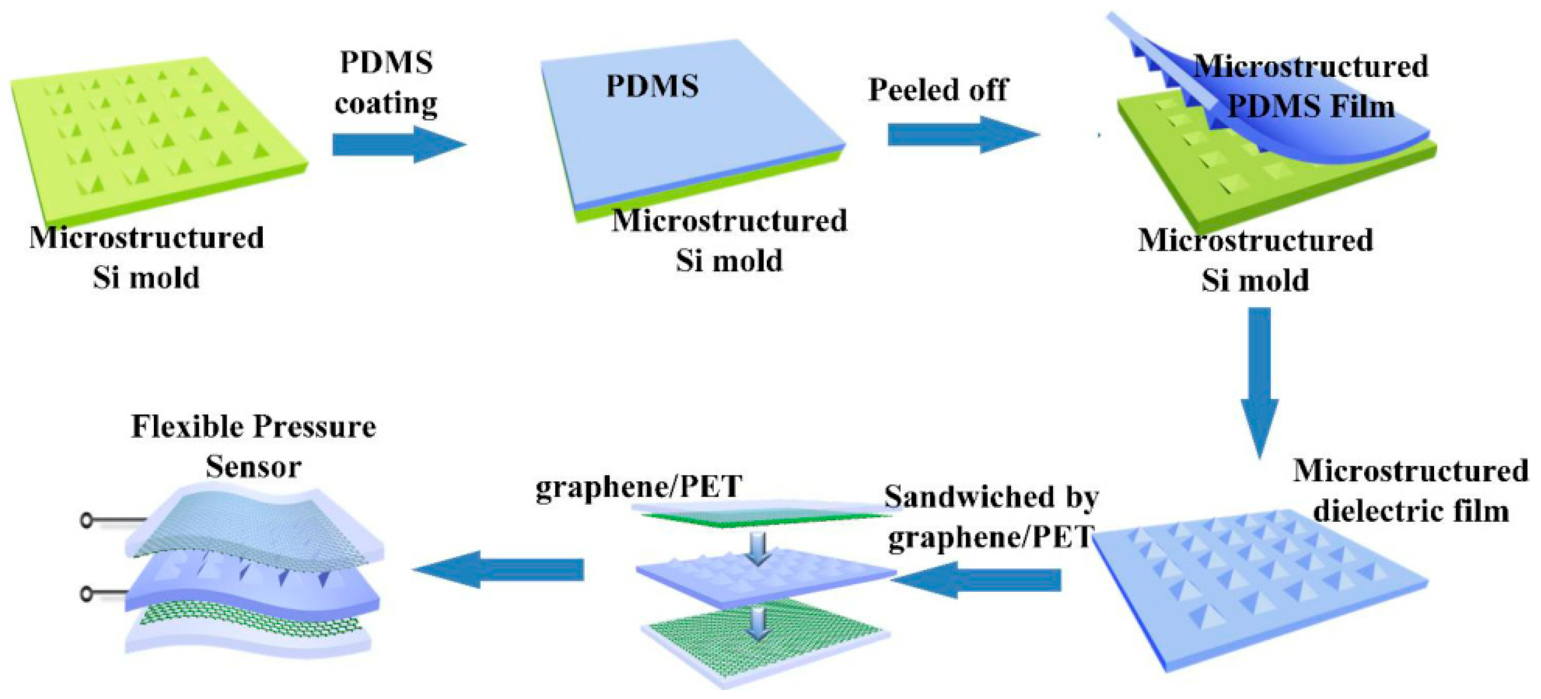
  96. Luo, S.; Yang, J.; Song, X.; Zhou, X.; Yu, L.; Sun, T.; Yu, C.; Huang, D.; Du, C.; Wei, D. Tunable-Sensitivity flexible pressure sensor based on graphene transparent electrode. Solid-State Electron. 2018, 145, 29–33. [Google Scholar] [CrossRef]
  97. Garg, R.; Elmas, S.; Nann, T.; Andersson, M.R. Deposition Methods of Graphene as Electrode Material for Organic Solar Cells. Adv. Energy Mater. 2017, 7, 1601393. [Google Scholar] [CrossRef]
  98. Li, S.; Ma, S.; Zhang, Y.; Zhao, L.; Yang, H.; Jin, R. Metal-organic interface engineering for coupling palladium nanocrystals over functionalized graphene as an advanced electrocatalyst of methanol and ethanol oxidation. J. Colloid Interface Sci. 2021, 588, 384–392. [Google Scholar] [CrossRef]
  99. Takagi, Y.; Yamazaki, S.; Nakatsuji, K.; Hirayama, H. Size, shape, and number density of deposits in the graphene solution liquid droplet method. Mater. Today Commun. 2017, 13, 65–71. [Google Scholar] [CrossRef]
  100. Yuan, G.; Lin, D.; Wang, Y.; Huang, X.; Chen, W.; Xie, X.; Zong, J.; Yuan, Q.-Q.; Zheng, H.; Wang, D.; et al. Proton-assisted growth of ultra-flat graphene films. Nat. Cell Biol. 2020, 577, 204–208. [Google Scholar] [CrossRef]
  101. Tiwari, S.; Purabgola, A.; Kandasubramanian, B. Functionalised graphene as flexible electrodes for polymer photovoltaics. J. Alloys Compd. 2020, 825, 153954. [Google Scholar] [CrossRef]
  102. Du, J.; Zhang, D.; Wang, X.; Jin, H.; Zhang, W.; Tong, B.; Liu, Y.; Burn, P.L.; Cheng, H.-M.; Ren, W. Extremely efficient flexible organic solar cells with a graphene transparent anode: Dependence on number of layers and doping of graphene. Carbon 2021, 171, 350–358. [Google Scholar] [CrossRef]
  103. Song, Z.; Li, W.; Bao, Y.; Kong, H.; Gan, S.; Wang, W.; Liu, Z.; Ma, Y.; Han, D.; Niu, L. Space-Confined Graphene Films for Pressure-Sensing Applications. ACS Appl. Nano Mater. 2020, 3, 1731–1740. [Google Scholar] [CrossRef]
  104. Tajik, S.; Beitollahi, H.; Nejad, F.G.; Shoaie, I.S.; Khalilzadeh, M.A.; Asl, M.S.; Van Le, Q.; Zhang, K.; Jang, H.W.; Shokouhimehr, M. Recent developments in conducting polymers: Applications for electrochemistry. RSC Adv. 2020, 10, 37834–37856. [Google Scholar] [CrossRef]
  105. Bao, H.; Wu, Y.; Liu, J.; Hua, X.; Lai, G.; Yang, X. Polyester–Polysiloxane Hyperbranched Block Polymers for Transparent Flexible Materials. ACS Omega 2020, 5, 29513–29519. [Google Scholar] [CrossRef]
  106. Cheng, M.; Meng, Y.-N.; Wei, Z.-X. Conducting Polymer Nanostructures and their Derivatives for Flexible Supercapacitors. Isr. J. Chem. 2018, 58, 1299–1314. [Google Scholar] [CrossRef]
  107. Zhang, H.; Yao, M.; Wei, J.; Zhang, Y.; Zhang, S.; Gao, Y.; Li, J.; Lu, P.; Yang, B.; Ma, Y. Stable p/n-Dopable Conducting Redox Polymers for High-Voltage Pseudocapacitor Electrode Materials: Structure-Performance Relationship and Detailed Investigation into Charge-Trapping Effect. Adv. Energy Mater. 2017, 7, 10. [Google Scholar] [CrossRef]
  108. Meer, S.; Kausar, A.; Iqbal, T. Trends in Conducting Polymer and Hybrids of Conducting Polymer/Carbon Nanotube: A Review. Polym. Technol. Eng. 2016, 55, 1416–1440. [Google Scholar] [CrossRef]
  109. Asyraf, M.; Anwar, M.; Sheng, L.M.; Danquah, M.K. Recent Development of Nanomaterial-Doped Conductive Polymers. JOM 2017, 69, 2515–2523. [Google Scholar] [CrossRef]
  110. Chai, Y.; Ma, X.; Jiang, Y.; Xiao, D.; Xue, M. Realizing Long-Range Orientational Order in Conjugated Polymers via Solventless Polymerization Strategy. Macromol. Chem. Phys. 2020, 221, 6. [Google Scholar] [CrossRef]
  111. Zhang, Q.; Dong, H.; Hu, W. Electrochemical polymerization for two-dimensional conjugated polymers. J. Mater. Chem. C 2018, 6, 10672–10686. [Google Scholar] [CrossRef]
  112. Kwon, G.; Kim, S.-H.; Kim, D.; Lee, K.; Jeon, Y.; Park, C.-S.; You, J. Vapor phase polymerization for electronically conductive nanopaper based on bacterial cellulose/poly(3,4-ethylenedioxythiophene). Carbohydr. Polym. 2021, 257, 117658. [Google Scholar] [CrossRef] [PubMed]
  113. Khokhar, D.; Jadoun, S.; Arif, R.; Jabin, S. Functionalization of conducting polymers and their applications in optoelectronics. Polym. Technol. Mater. 2021, 60, 463–485. [Google Scholar] [CrossRef]
  114. Yuk, H.; Lu, B.; Lin, S.; Qu, K.; Xu, J.; Luo, J.; Zhao, X. 3D printing of conducting polymers. Nat. Commun. 2020, 11, 1–8. [Google Scholar] [CrossRef] [Green Version]
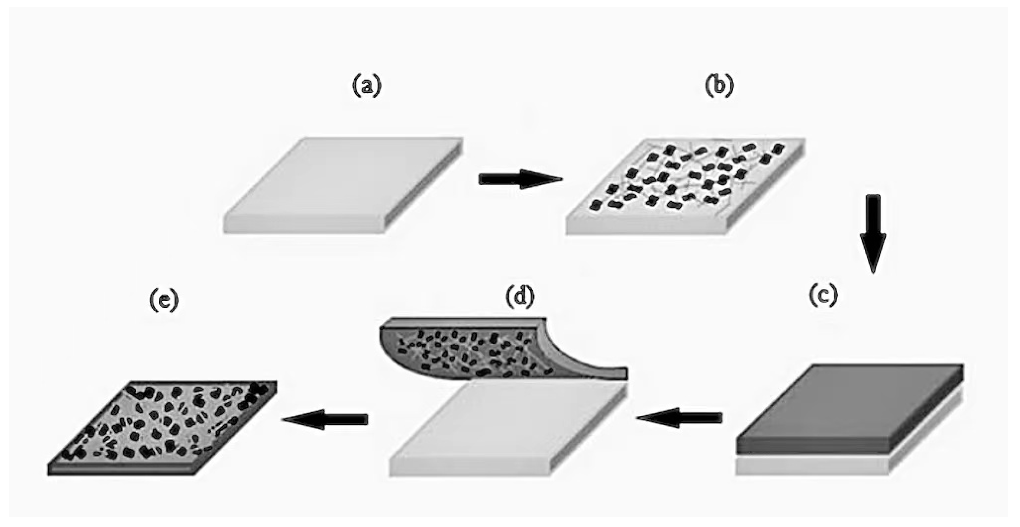
  115. Lim, C.K.; Lee, Y.S.; Choa, S.H.; Lee, D.Y.; Park, L.S.; Nam, S.Y. Effect of Polymer Binder on the Transparent Conducting Electrodes on Stretchable Film Fabricated by Screen Printing of Silver Paste. Int. J. Polym. Sci. 2017, 2017, 1–6. [Google Scholar] [CrossRef] [Green Version]
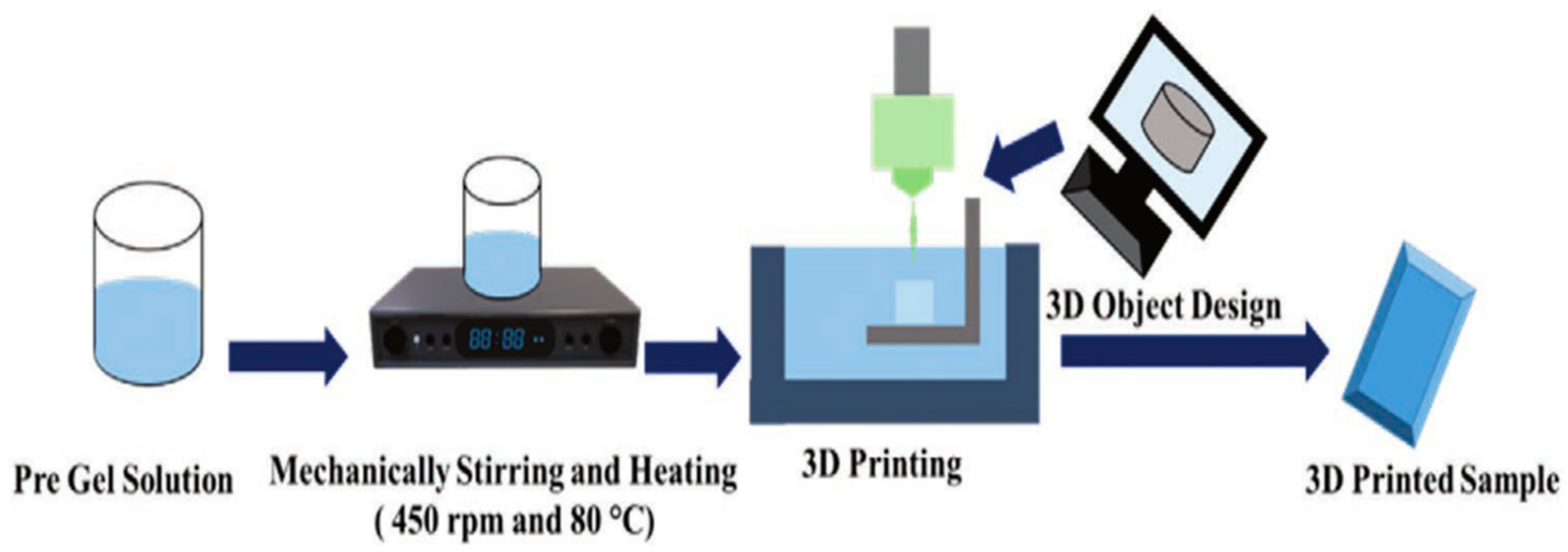
  116. Rahman, M.S.; Shiblee MN, I.; Ahmed, K.; Khosla, A.; Ogawa, J.; Kawakami, M.; Furukawa, H. Flexible and Conductive 3D Printable Polyvinylidene Fluoride and Poly(N,N-dimethylacrylamide) Based Gel Polymer Electrolytes. Macromol. Mater. Eng. 2020, 305, 2000262. [Google Scholar] [CrossRef]
  117. Zhu, J.; Han, D.; Wu, X.; Ting, J.; Du, S.; Arias, A.C. Highly Flexible Transparent Micromesh Electrodes via Blade-Coated Polymer Networks for Organic Light-Emitting Diodes. ACS Appl. Mater. Interfaces 2020, 12, 31687–31695. [Google Scholar] [CrossRef]
  118. Kumar, P.; Woon, K.L.; Wong, W.S.; Saheed, M.S.M.; Burhanudin, Z.A. Hybrid film of single-layer graphene and carbon nanotube as transparent conductive electrode for organic light emitting diode. Synth. Met. 2019, 257, 116186. [Google Scholar] [CrossRef]
  119. Lee, S.; Kim, M.; Cho, S.-Y.; Lee, D.-J.; Kim, H.-M.; Kim, K.-B. Electrical properties of graphene/In2O3 bilayer with remarkable uniformity as transparent conducting electrode. Nanotechnology 2019, 31, 095708. [Google Scholar] [CrossRef]
  120. Yang, M.K.; Lee, J.-K. CNT/AgNW Multilayer Electrodes on Flexible Organic Solar Cells. Electron. Mater. Lett. 2020, 16, 573–578. [Google Scholar] [CrossRef]
  121. Cui, J.; Mei, H.; Zhang, J.; Fan, Z.; Yang, J.; Wang, W.; Tohmyoh, H.; Mei, X. Interfacial Contact Behavior between CNTs and AgNW with Molecular Dynamics Simulation. Materials 2020, 13, 1290. [Google Scholar] [CrossRef] [Green Version]
  122. Ma, C.; Liu, H.; Teng, C.; Li, L.; Zhu, Y.; Yang, H.; Jiang, L. Wetting-Induced Fabrication of Graphene Hybrid with Conducting Polymers for High-Performance Flexible Transparent Electrodes. ACS Appl. Mater. Interfaces 2020, 12, 55372–55381. [Google Scholar] [CrossRef] [PubMed]
  123. Kim, M.; Nabeya, S.; Han, S.M.; Kim, M.S.; Lee, S.; Kim, H.M.; Cho, S.Y.; Lee, D.J.; Kim, S.H.; Kim, K.B. Selective Atomic Layer Deposition of Metals on Graphene for Transparent Conducting Electrode Application. ACS Appl. Mater. Interfaces 2020, 12, 14331–14340. [Google Scholar] [CrossRef] [PubMed]
  124. Shan, Y.-F.; Yang, K.; Li, Z.-X.; Wang, X.-X.; Li, H.; Cui, Y.-Y. Conductive Film with Flexible and Stretchable Capability for Sensor Application and Stealth Information Transmission. Chin. J. Polym. Sci. 2021, 39, 164–173. [Google Scholar] [CrossRef]
  125. Vukmirović, J.; Nesterović, A.; Stijepović, I.; Milanović, M.; Omerović, N.; Bajac, B.; Bobić, J.; Srdić, V.V. Fabrication of BaTiO3-based thin film heterostructures with ring electrodes by low cost deposition techniques. J. Mater. Sci. Mater. Electron. 2019, 30, 14995–15004. [Google Scholar] [CrossRef]
  126. Gonçalves, S.A.P.; Nunes, J.S.; Oliveira, J.; Pereira, N.; Hilliou, L.; Costa, C.M.; Lanceros-Mendez, S. Environmentally Friendly Printable Piezoelectric Inks and Their Application in the Development of All-Printed Touch Screens. ACS Appl. Electron. Mater. 2019, 1, 1678–1687. [Google Scholar] [CrossRef]
  127. Lakshmi-Narayana, A.; Prakash, N.G.; Dhananjaya, M.; Hussain, O.M.; Qiu, Y.J.; Julien, C.M. Pulsed laser–deposited Li2TiO3 thin film electrodes for energy storage. J. Solid State Electrochem. 2020, 24, 1371–1385. [Google Scholar] [CrossRef]
  128. Jung, H.W. Special Issue on “Thin Film Processes”. Processes 2020, 8, 564. [Google Scholar] [CrossRef]
  129. Zhu, Z.; Zhang, J.; Guo, D.; Ning, H.; Zhou, S.; Liang, Z.; Yao, R.; Wang, Y.; Lu, X.; Peng, J. Functional Metal Oxide Ink Systems for Drop-on-Demand Printed Thin-Film Transistors. Langmuir 2020, 36, 8655–8667. [Google Scholar] [CrossRef]
  130. Stanojev, J.; Bajac, B.; Cvejic, Z.; Matovic, J.; Srdic, V.V. Development of MWCNT thin film electrode transparent in the mid-IR range. Ceram. Int. 2020, 46, 11340–11345. [Google Scholar] [CrossRef]
  131. Kim, G.W.; Shin, D.; Yang, M. Optical Property Change of Silver Nanowire Thin Films in Laser Patterning Process. Int. J. Precis. Eng. Manuf. 2020, 21, 301–308. [Google Scholar] [CrossRef]
  132. Lee, G.J.; Heo, S.J.; Lee, S.; Yang, J.H.; Jun, B.O.; Kim, H.S.; Jang, J.E. Stress Release Effect of Micro-hole Arrays for Flexible Electrodes and Thin Film Transistors. ACS Appl. Mater. Interfaces 2020, 12, 19226–19234. [Google Scholar] [CrossRef] [PubMed]
  133. Chen, J.; Yang, L.; Han, Y.; Bao, Y.-H.; Zhang, K.-L.; Li, X.; Pang, J.; Chen, H.-S.; Song, W.-L.; Wei, Y.-J.; et al. An in situ system for simultaneous stress measurement and optical observation of silicon thin film electrodes. J. Power Sources 2019, 444, 227227. [Google Scholar] [CrossRef]
  134. Meng, L.; Xu, Q.; Dan, L.; Wang, X. Single-Walled Carbon Nanotube Based Triboelectric Flexible Touch Sensors. J. Electron. Mater. 2019, 48, 7411–7416. [Google Scholar] [CrossRef]
  135. Yang, M.; Xu, K.; Wang, L. Flexible touch sensor fabricated by double-sided nanoimprint lithography metal transfer. Nanotechnology 2020, 31, 315302. [Google Scholar] [CrossRef] [PubMed]
  136. Kim, S.; Phung, T.H.; Kim, S.; Rahman, K.; Kwon, K. Low-Cost Fabrication Method for Thin, Flexible, and Transparent Touch Screen Sensors. Adv. Mater. Technol. 2020, 2000441. [Google Scholar] [CrossRef]
  137. Choi, H.B.; Oh, J.; Kim, Y.; Pyatykh, M.; Yang, J.C.; Ryu, S.; Park, S. Transparent Pressure Sensor with High Linearity over a Wide Pressure Range for 3D Touch Screen Applications. ACS Appl. Mater. Interfaces 2020, 12, 16691–16699. [Google Scholar] [CrossRef]
  138. Shi, Y.; He, L.; Deng, Q.; Liu, Q.; Li, L.; Wang, W.; Xin, Z.; Liu, R. Synthesis and Applications of Silver Nanowires for Transparent Conductive Films. Micromachines 2019, 10, 330. [Google Scholar] [CrossRef] [Green Version]
  139. Qiu, T.; Luo, B.; Akinoglu, E.M.; Yun, J.; Gentle, I.R.; Wang, L. Trilayer Nanomesh Films with Tunable Wettability as Highly Transparent, Flexible, and Recyclable Electrodes. Adv. Funct. Mater. 2020, 30, 2002556. [Google Scholar] [CrossRef]
  140. Sarjidan, M.A.M.; Majid, W.H.A. Prospect of silver nanowire (AgNW) in development of simple and cost-effective vertical organic light-emitting transistors. Appl. Phys. A 2019, 125, 871. [Google Scholar] [CrossRef]
  141. Jiang, X.; Song, Z.; Liu, G.; Ma, Y.; Wang, A.; Guo, Y.; Du, Z. AgNWs/AZO composite electrode for transparent inverted ZnCdSeS/ZnS quantum dot light-emitting diodes. Nanotechnology 2019, 31, 055201. [Google Scholar] [CrossRef] [PubMed]
  142. Gu, Z.-Z.; Tian, Y.; Geng, H.-Z.; Rhen, D.S.; Ethiraj, A.S.; Zhang, X.; Jing, L.-C.; Wang, T.; Xu, Z.-H.; Yuan, X.-T. Highly conductive sandwich-structured CNT/PEDOT:PSS/CNT transparent conductive films for OLED electrodes. Appl. Nanosci. 2019, 9, 1971–1979. [Google Scholar] [CrossRef]
  143. Badkoobehhezaveh, A.M.; Hopmann, E.; Elezzabi, A.Y. Flexible Multicolor Electroluminescent Devices on Cellulose Nanocrystal Platform. Adv. Eng. Mater. 2020, 22, 1901452. [Google Scholar] [CrossRef]
  144. Zuo, Y.; Shi, X.; Zhou, X.; Xu, X.; Wang, J.; Chen, P.; Sun, X.; Peng, H. Flexible Color-Tunable Electroluminescent Devices by Designing Dielectric-Distinguishing Double-Stacked Emissive Layers. Adv. Funct. Mater. 2020, 30, 2005200. [Google Scholar] [CrossRef]
  145. Zhou, Y.; Zhao, C.; Wang, J.; Li, Y.; Li, C.; Zhu, H.; Feng, S.; Cao, S.; Kong, D. Stretchable High-Permittivity Nanocomposites for Epidermal Alternating-Current Electroluminescent Displays. ACS Mater. Lett. 2019, 1, 511–518. [Google Scholar] [CrossRef]
  146. Shim, H.; Allabergenov, B.; Kim, J.; Noh, H.Y.; Lyu, H.K.; Lee, M.J.; Choi, B. Highly Bright Flexible Electroluminescent Devices with Retroreflective Electrodes. Adv. Mater. Technol. 2017, 2, 1700040. [Google Scholar] [CrossRef]
  147. Yakoh, A.; Siangproh, W.; Chailapakul, O.; Ngamrojanavanich, N. Optical Bioelectronic Device Based on a Screen-Printed Electroluminescent Transducer. ACS Appl. Mater. Interfaces 2020, 12, 22543–22551. [Google Scholar] [CrossRef] [PubMed]
  148. Lim, Y.-W.; Jin, J.; Bae, B.-S. Optically Transparent Multiscale Composite Films for Flexible and Wearable Electronics. Adv. Mater. 2020, 32, e1907143. [Google Scholar] [CrossRef]
  149. Li, P.; Zhao, Y.; Ma, J.; Yang, Y.; Xu, H.; Liu, Y. Facile Fabrication of Ultraflexible Transparent Electrodes Using Embedded Copper Networks for Wearable Pressure Sensors. Adv. Mater. Technol. 2020, 5, 1900823. [Google Scholar] [CrossRef]
  150. Zhao, P.; Zhang, R.; Tong, Y.; Zhao, X.; Zhang, T.; Tang, Q.; Liu, Y. Strain-Discriminable Pressure/Proximity Sensing of Transparent Stretchable Electronic Skin Based on PEDOT:PSS/SWCNT Electrodes. ACS Appl. Mater. Interfaces 2020, 12, 55083–55093. [Google Scholar] [CrossRef]
  151. Afroj, S.; Tan, S.; Abdelkader, A.M.; Novoselov, K.S.; Karim, N. Highly Conductive, Scalable, and Machine Washable Graphene-Based E-Textiles for Multifunctional Wearable Electronic Applications. Adv. Funct. Mater. 2020, 30, 2000293. [Google Scholar] [CrossRef] [Green Version]
  152. Mokhtari, F.; Spinks, G.M.; Fay, C.; Cheng, Z.; Raad, R.; Xi, J.; Foroughi, J. Wearable Electronic Textiles from Nanostructured Piezoelectric Fibers. Adv. Mater. Technol. 2020, 5, 1900900. [Google Scholar] [CrossRef]
  153. Wu, C.; Kim, T.W.; Guo, T.; Li, F. Wearable ultra-lightweight solar textiles based on transparent electronic fabrics. Nano Energy 2017, 32, 367–373. [Google Scholar] [CrossRef]
  154. Suriani, A.B.; Muqoyyanah; Mohamed, A.; Alfarisa, S.; Mamat, M.H.; Ahmad, M.K.; Birowosuto, M.D.; Soga, T. Synthesis, transfer and application of graphene as a transparent conductive film: A review. Bull. Mater. Sci. 2020, 43, 310. [Google Scholar] [CrossRef]
  155. Yao, Z.; Qu, D.; Guo, Y.; Huang, H. Flexible, stable and indium-free perovskite solar cells using solution-processed transparent graphene electrodes. J. Mater. Sci. 2019, 54, 11564–11573. [Google Scholar] [CrossRef]
  156. Guo, T.; Zhang, G.; Zhang, H.; Su, X.; Chen, X.; Wan, J.; Wu, H.; Liu, C. High-quality-factor flexible and transparent capacitors with Cr-Au nanomeshes as bottom electrodes. Nanotechnology 2019, 30, 284001. [Google Scholar] [CrossRef]
  157. Qin, Y.; Li, J.; Jin, X.; Jiao, S.; Chen, Y.; Cai, W.; Cao, R. Anthraquinone-functionalized graphene framework for supercapacitors and lithium batteries. Ceram. Int. 2020, 46, 15379–15384. [Google Scholar] [CrossRef]
  158. Azman, N.H.N.; Nazir, S.M.; Ngee, L.H.; Sulaiman, Y. Graphene-based ternary composites for supercapacitors. Int. J. Energy Res. 2018, 42, 2104–2116. [Google Scholar] [CrossRef]
  159. Zhao, W.; Jiang, M.; Wang, W.; Liu, S.; Huang, W.; Zhao, Q. Flexible Transparent Supercapacitors: Materials and Devices. Adv. Funct. Mater. 2021, 31, 2009136. [Google Scholar] [CrossRef]
  160. Zhao, Y.; Liu, J.; Horn, M.; Motta, N.; Hu, M.; Li, Y. Recent advancements in metal organic framework based electrodes for supercapacitors. Sci. China Mater. 2018, 61, 159–184. [Google Scholar] [CrossRef] [Green Version]
  161. Liu, T.; Yan, R.; Huang, H.; Pan, L.; Cao, X.; Demello, A.; Niederberger, M. A Micromolding Method for Transparent and Flexible Thin-Film Supercapacitors and Hybrid Supercapacitors. Adv. Funct. Mater. 2020, 30, 2004410. [Google Scholar] [CrossRef]
  162. Zhou, B.; Su, M.; Yang, D.; Han, G.; Feng, Y.; Wang, B.; Ma, J.; Ma, J.; Liu, C.; Shen, C. Flexible MXene/Silver Nanowire-Based Transparent Conductive Film with Electromagnetic Interference Shielding and Electro-Photo-Thermal Performance. ACS Appl. Mater. Interfaces 2020, 12, 40859–40869. [Google Scholar] [CrossRef] [PubMed]
  163. Chen, W.; Liu, L.-X.; Zhang, H.-B.; Yu, Z.-Z. Flexible, Transparent, and Conductive Ti3C2Tx MXene–Silver Nanowire Films with Smart Acoustic Sensitivity for High-Performance Electromagnetic Interference Shielding. ACS Nano 2020, 14, 16643–16653. [Google Scholar] [CrossRef] [PubMed]
Figure 1. (a) SEM and (b) TEM images of AgNWs [20]; (c,d) SEM images of CuNWs at different magnifications [41]; (e) schematic diagram of AgNW synthesis process [20]; (f) schematic diagram of a healable nanocomposite conductor based on CuNWs and DA-PU [40].
Crystals 11 00511 g001
Figure 2. (a) Schematic sketch of metal film deposition (conventional deposition and new multilayer deposition strategy) [55]; (b) schematic structure of the ZnO/Ag/ZnO transparent heater fabricated on top of a transparent PI substrate [50]; (c) schematic architecture of a stretchable ACEL device before and after stretching; (d) photographs and OM images of patterned ACUF/anisotropic conductive ultrathin film (ACUF)/Au electrodes and their interconnection [11].
Crystals 11 00511 g002
Figure 3. (a) Schematic illustration of the preparation of transparent and conductive Ag mesh films; (b,d) SEM images of Ag mesh films fabricated with Ag nanoparticle ink after a sintering process; (c,e) SEM images of Ag mesh films fabricated with Ag nanoparticle ink after a coupling process [68].
Crystals 11 00511 g003
Figure 4. (a) Schematic illustration of the preparation of copper meshes on a flexible substrate; (b) SEM image of copper nanoparticles; (c) evolution of sheet resistance and transparency at 550 nm wavelength with mesh size; (d) evolution of sheet resistance and transparency at 550 nm wavelength with line width; (e) sheet resistance variation (R/R0) versus the number of cycles of repeated bending to a radius of 3 mm [69].
Crystals 11 00511 g004
Figure 5. (a) TEM image of CNTs [73]; (b) representation of the layer-by-layer schematic process and multilayer transfer process [88].
Crystals 11 00511 g005
Figure 6. The preparation processes of a Polydimethylsiloxane (PDMS) dielectric layer with micro-pyramid structures and pressure sensor-based graphene electrodes [96].
Crystals 11 00511 g006
Figure 7. Schematic diagram of PVDF/DMAAm gel synthesis process using 3D gel printer [116].
Crystals 11 00511 g007
Figure 8. Schematic representation of nanocomposite thin film production: (a) glass substrate; (b) spin-coated glass with conductive material; (c) polymeric material-coated conductive glass; (d) removal of conductive polymeric film from glass; (e) self-standing conductive polymeric layer [9].
Crystals 11 00511 g008
Figure 9. Radar map of different material properties.
Crystals 11 00511 g009
Figure 10. Concept of metal atomic layer deposition (ALD) on graphene. (a) Doping graphene by charge transfer between graphene and metal. (b) Selective deposition of Pt by ALD on graphene [123].
Crystals 11 00511 g010
Figure 11. The applications of FTEs.
Crystals 11 00511 g011
Table 1. The advantages and disadvantages of traditional methods.
MethodAdvantageDisadvantage
CVDFilm is very pure and denseReaction at high temperature; difficulty in mass production; toxic byproducts
PVDGood film uniformity; high process automaticityDifficulty in mass production
Spin-coatingFilm thickness uniformityLoss of large quantities of solution
SprayingNo loss of solutionDifficulties in process optimization of solvent mixing and solution adjustment
CastHigh crystallinityPoor homogeneity of film
InkjetComputer control; material loss is small; fast production of multi-layer structuresInk requirements high conditions; droplet coalescence
Screen printingSimple manufacturing processThick film
NanoimprintThe scale of tens of nanometers patterning can be obtained at normal temperature and pressureThe process is not mature; the equipment is expensive
DippingLarge area film formationThick film
LBControlled production of monolayer and layer by layer accumulationThe corresponding materials are limited
Self-assemblyMonomolecular membrane with high orientationThe corresponding materials are limited
Publisher’s Note: MDPI stays neutral with regard to jurisdictional claims in published maps and institutional affiliations.

