
A Review on MoS2 Properties, Synthesis, Sensing Applications and Challenges


Abstract
:1. Introduction
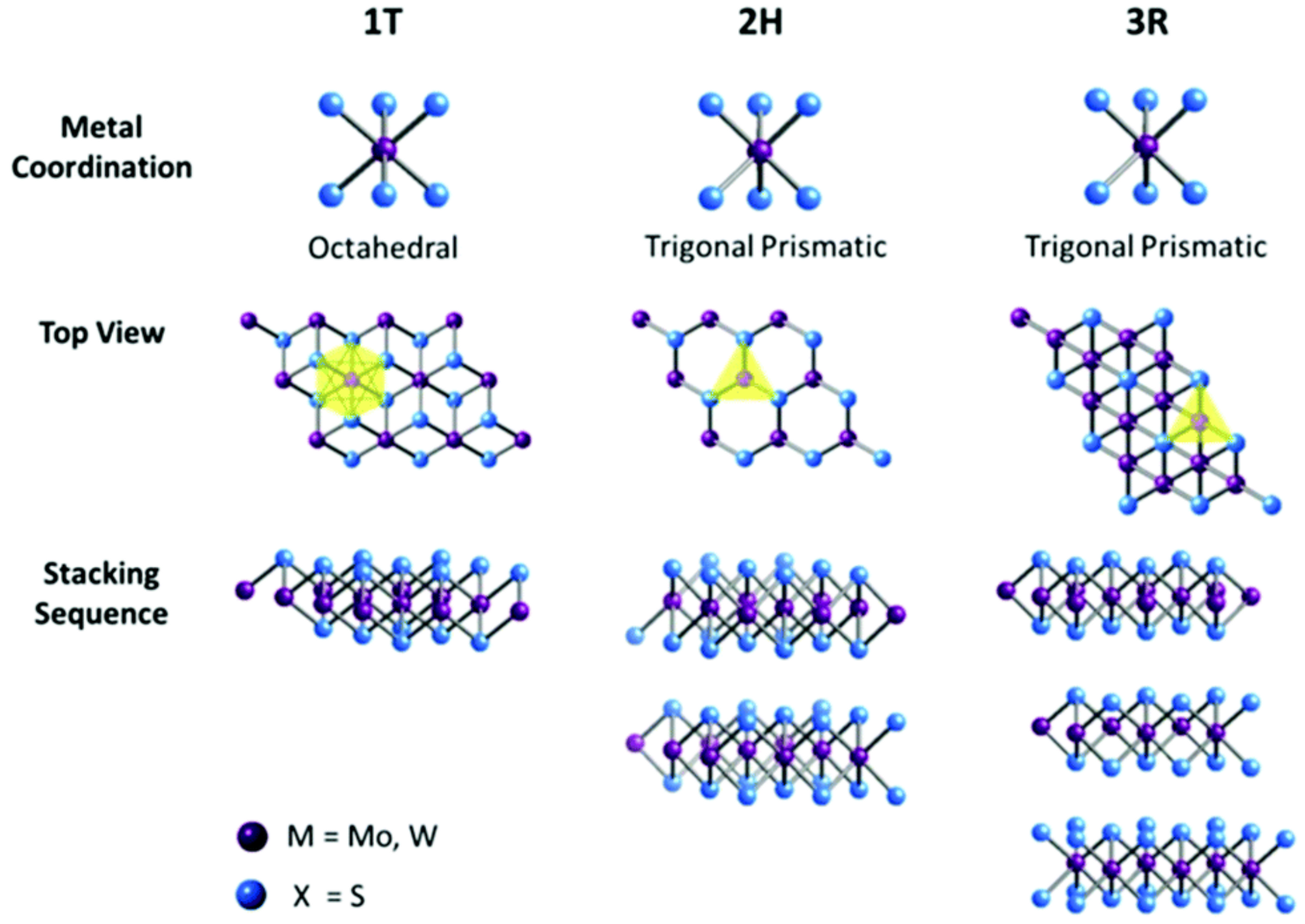
2. Structure and Properties
2.1. Optical Properties
2.2. Mechanical Properties
2.3. Electronic Properties
2.4. Magnetic Properties (Spintronics)
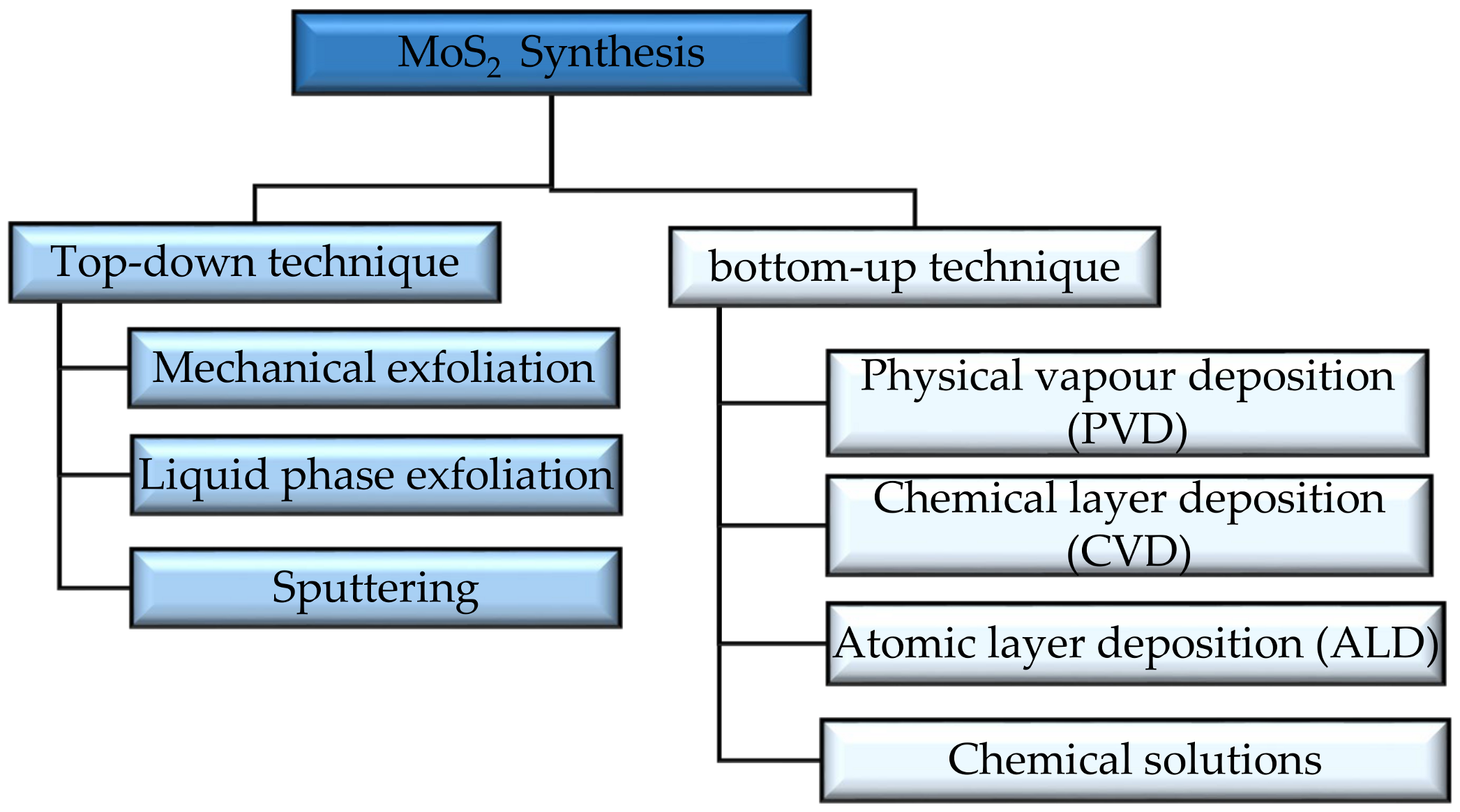
3. Synthesis
4. Applications
4.1. Electronics Applications
4.2. Medical Applications
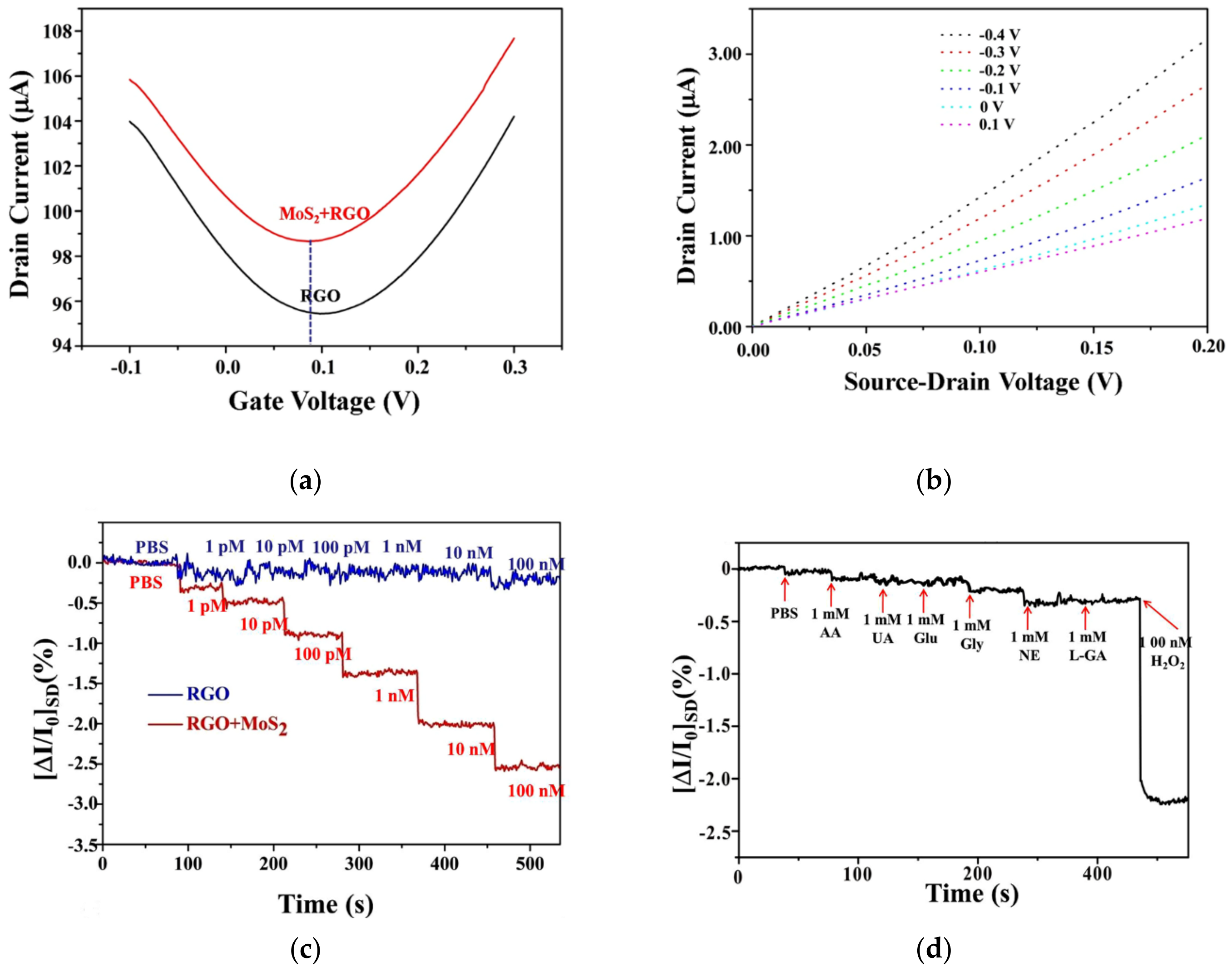
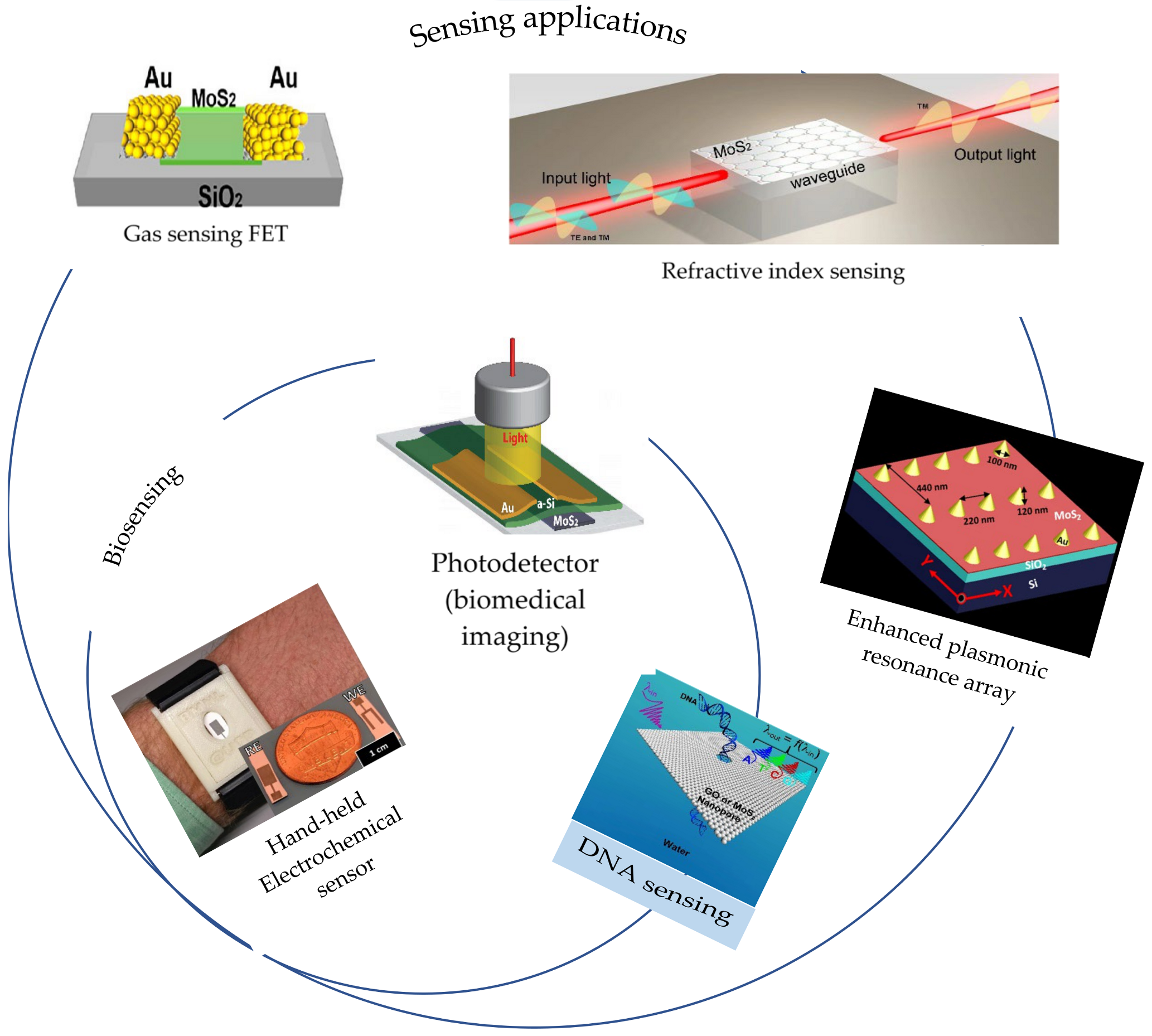
4.3. Sensing Applications
4.4. Miscellaneous Applications
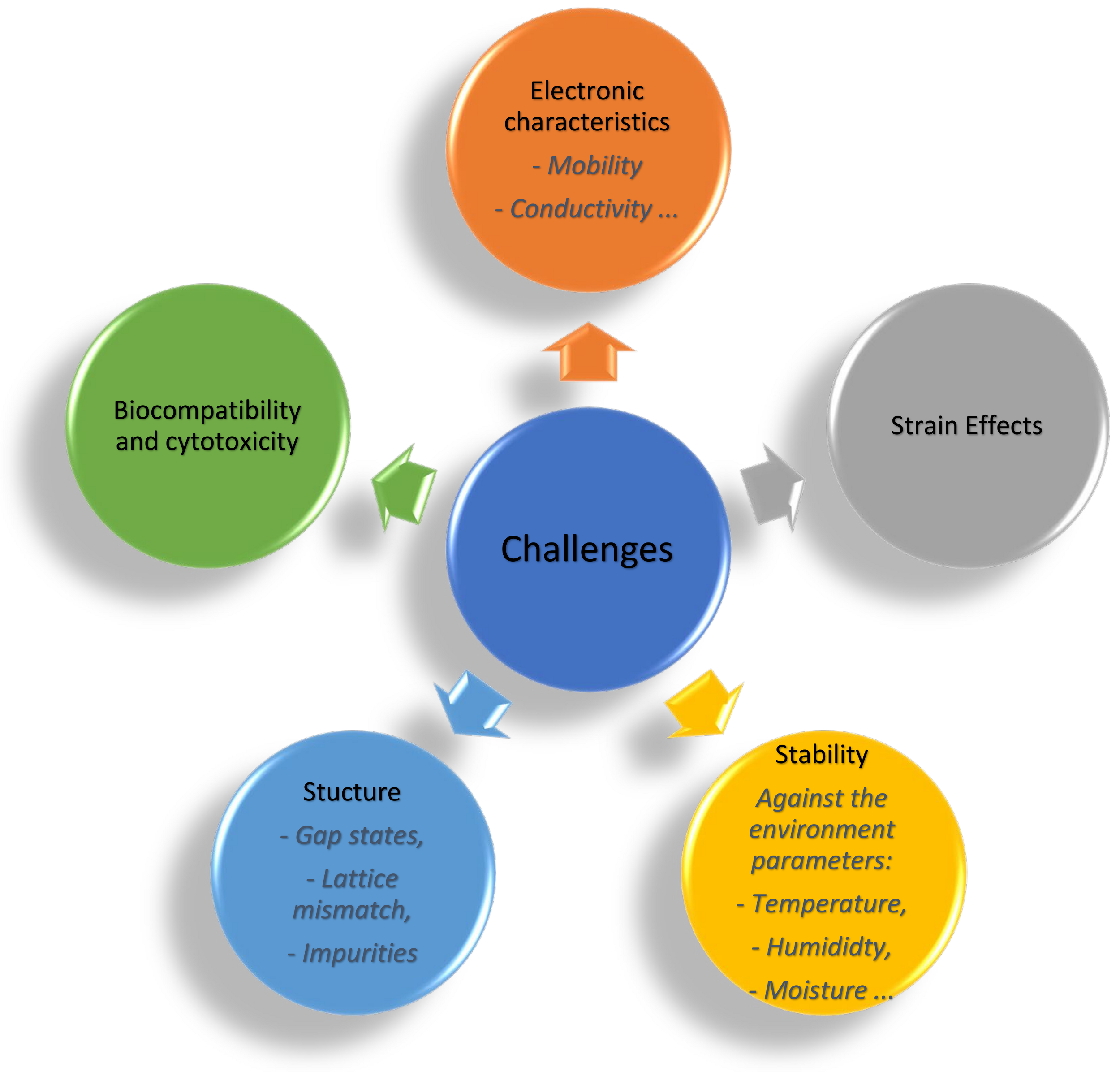
5. Challenges
6. Conclusions
Author Contributions
Funding
Institutional Review Board Statement
Informed Consent Statement
Data Availability Statement
Conflicts of Interest
References
- He, Z.; Que, W. Molybdenum Disulfide Nanomaterials: Structures, Properties, Synthesis and Recent Progress on Hydrogen Evolution Reaction. Appl. Mater. Today 2016, 3, 23–56. [Google Scholar] [CrossRef]
- Hersam, M.C. Emerging Device Applications for Two-Dimensional Nanomaterial Heterostructures. In Proceedings of the 2015 73rd Annual Device Research Conference (DRC), Columbus, OH, USA, 21–24 June 2015; IEEE: Columbus, OH, USA, 2015; p. 209. [Google Scholar]
- Zhao, G.-Y.; Deng, H.; Tyree, N.; Guy, M.; Lisfi, A.; Peng, Q.; Yan, J.-A.; Wang, C.; Lan, Y. Recent Progress on Irradiation-Induced Defect Engineering of Two-Dimensional 2H-MoS2 Few Layers. Appl. Sci. 2019, 9, 678. [Google Scholar] [CrossRef] [Green Version]
- Del Alamo, J.A. Nanometre-Scale Electronics with III-V Compound Semiconductors. Nature 2011, 479, 317–323. [Google Scholar] [CrossRef] [PubMed]
- Geim, A.K.; Grigorieva, I.V. Van Der Waals Heterostructures. Nature 2013, 499, 419–425. [Google Scholar] [CrossRef]
- Current, M.I. Process and Metrology Challenges for Nano-Scale Electronics. In Proceedings of the 2016 IEEE Workshop on Microelectronics and Electron Devices (WMED), Boise, ID, USA, 15 April 2016; IEEE: Boise, ID, USA, 2016; pp. 1–5. [Google Scholar]
- Butler, S.Z.; Hollen, S.M.; Cao, L.; Cui, Y.; Gupta, J.A.; Gutiérrez, H.R.; Heinz, T.F.; Hong, S.S.; Huang, J.; Ismach, A.F.; et al. Progress, Challenges, and Opportunities in Two-Dimensional Materials Beyond Graphene. ACS Nano 2013, 7, 2898–2926. [Google Scholar] [CrossRef]
- Bhat, N. Tunable Steep Slope MoS2 Transistor. In Proceedings of the 2018 IEEE International Conference on Semiconductor Electronics (ICSE), Kuala Lumpur, Malaysia, 15–17 August 2018; IEEE: Kuala Lumpur, 2018; p. C1. [Google Scholar]
- Novoselov, K. Beyond the Wonder Material. Phys. World 2009, 22, 27–30. [Google Scholar] [CrossRef]
- Moutaouakil, A.E.; Kang, H.-C.; Handa, H.; Fukidome, H.; Suemitsu, T.; Sano, E.; Suemitsu, M.; Otsuji, T. Room Temperature Logic Inverter on Epitaxial Graphene-on-Silicon Device. Jpn. J. Appl. Phys. 2011, 50, 070113. [Google Scholar] [CrossRef] [Green Version]
- Yoo, G.; Lee, S.; Yoo, B.; Han, C.; Kim, S.; Oh, M.S. Electrical Contact Analysis of Multilayer MoS2 Transistor With Molybdenum Source/Drain Electrodes. IEEE Electron Device Lett. 2015, 36, 1215–1218. [Google Scholar] [CrossRef]
- Das, S. 2D Materials for Ubiquitous Electronics. In Proceedings of the 2018 IEEE 2nd Electron Devices Technology and Manufacturing Conference (EDTM), Kobe, Japan, 13–16 March 2018; IEEE: Kobe, Japan, 2018; pp. 19–20. [Google Scholar]
- Hiraki, A. Recent Developments on Metal-Silicon Interfaces. Appl. Surf. Sci. 1992, 56–58, 370–381. [Google Scholar] [CrossRef]
- Desai, S.B.; Madhvapathy, S.R.; Sachid, A.B.; Llinas, J.P.; Wang, Q.; Ahn, G.H.; Pitner, G.; Kim, M.J.; Bokor, J.; Hu, C.; et al. MoS2 Transistors with 1-Nanometer Gate Lengths. Science 2016, 354, 99–102. [Google Scholar] [CrossRef] [Green Version]
- Hoefflinger, B. Nanolithography. In NANO-CHIPS 2030: On-Chip AI for an Efficient Data-Driven World; Murmann, B., Hoefflinger, B., Eds.; The Frontiers Collection; Springer International Publishing: Stanford, CA, USA, 2020; pp. 41–45. ISBN 978-3-030-18338-7. [Google Scholar]
- International Roadmap for Devices and Systems (IRDS™) 2020 Edition-IEEE IRDS™. Available online: https://irds.ieee.org/editions/2020 (accessed on 10 March 2021).
- Iwai, H.; Kakushima, K.; Wong, H. Challenges for future semiconductor manufacturing. Int. J. High Speed Electron. Syst. 2006, 43–81. [Google Scholar] [CrossRef] [Green Version]
- Irtegov, Y.; An, V.; Azhgikhin, M. Study of Nanostructured Metal Sulfides Produced by Self-Propagating High-Temperature Synthesis. In Proceedings of the 2012 7th International Forum on Strategic Technology (IFOST), Tomsk, Russia, 18–21 September 2012; IEEE: Tomsk, Russia, 2012; pp. 1–4. [Google Scholar]
- Sha, J.; Xu, W.; Yuan, Z.; Xu, B.; Chen, Y. Fabrication of Liquid-Gated Molybdenum Disulfide Field-Effect Transistor. In Proceedings of the 2017 IEEE 12th International Conference on Nano/Micro Engineered and Molecular Systems (NEMS), Los Angeles, CA, USA, 9–12 April 2017; IEEE: Los Angeles, CA, USA, 2017; pp. 788–791. [Google Scholar]
- Weng, X.; Neethirajan, S. Immunosensor Based on Antibody-Functionalized MoS2 for Rapid Detection of Avian Coronavirus on Cotton Thread. IEEE Sens. J. 2018, 18, 4358–4363. [Google Scholar] [CrossRef]
- Catalán-Gómez, S.; Briones, M.; Cortijo-Campos, S.; García-Mendiola, T.; de Andrés, A.; Garg, S.; Kung, P.; Lorenzo, E.; Pau, J.L.; Redondo-Cubero, A. Breast Cancer Biomarker Detection through the Photoluminescence of Epitaxial Monolayer MoS2 Flakes. Sci. Rep. 2020, 10, 16039. [Google Scholar] [CrossRef]
- Liu, Y.; Zhang, J.; Shen, Y.; Yan, J.; Hou, Z.; Mao, C. MoS2 quantum dots featured fluorescent biosensor for multiple detection of cancer. RSC Adv. 2017, 7, 54638–54643. [Google Scholar] [CrossRef] [Green Version]
- Kong, R.-M.; Ding, L.; Wang, Z.; You, J.; Qu, F. A Novel Aptamer-Functionalized MoS2 Nanosheet Fluorescent Biosensor for Sensitive Detection of Prostate Specific Antigen. Anal. Bioanal. Chem. 2015, 407, 369–377. [Google Scholar] [CrossRef]
- Sobanska, Z.; Zapor, L.; Szparaga, M.; Stepnik, M. Biological Effects of Molybdenum Compounds in Nanosized Forms under in Vitro and in Vivo Conditions. Int. J. Occup. Med. Environ. Health 2020, 33, 1–19. [Google Scholar] [CrossRef]
- Hossain, R.F.; Deaguero, I.G.; Boland, T.; Kaul, A.B. Biocompatible, Large-Format, Inkjet Printed Heterostructure MoS2-Graphene Photodetectors on Conformable Substrates. NPJ 2D Mater. Appl. 2017, 1, 28. [Google Scholar] [CrossRef] [Green Version]
- Liu, L.; Liu, Z.; Huang, P.; Wu, Z.; Jiang, S. Protein-Induced Ultrathin Molybdenum Disulfide (MoS2) Flakes for a Water-Based Lubricating System. RSC Adv. 2016, 6, 113315–113321. [Google Scholar] [CrossRef]
- Gupta, D.; Chauhan, V.; Kumar, R. A Comprehensive Review on Synthesis and Applications of Molybdenum Disulfide (MoS2) Material: Past and Recent Developments. Inorg. Chem. Commun. 2020, 121, 108200. [Google Scholar] [CrossRef]
- Li, X.; Zhu, H. Two-Dimensional MoS2: Properties, Preparation, and Applications. J. Mater. 2015, 1, 33–44. [Google Scholar] [CrossRef] [Green Version]
- Yadav, V.; Roy, S.; Singh, P.; Khan, Z.; Jaiswal, A. 2D MoS2-Based Nanomaterials for Therapeutic, Bioimaging, and Biosensing Applications. Small 2019, 15, 1803706. [Google Scholar] [CrossRef] [Green Version]
- Chodankar, N.R.; Nanjundan, A.K.; Losic, D.; Dubal, D.P.; Baek, J.-B. Graphene and Molybdenum Disulphide Hybrids for Energy Applications: An Update. Mater. Today Adv. 2020, 6, 100053. [Google Scholar] [CrossRef]
- Winer, W.O. Molybdenum Disulfide as a Lubricant: A Review of the Fundamental Knowledge. Wear 1967, 10, 422–452. [Google Scholar] [CrossRef] [Green Version]
- Jiao, Y.; Hafez, A.M.; Cao, D.; Mukhopadhyay, A.; Ma, Y.; Zhu, H. Metallic MoS2 for High Performance Energy Storage and Energy Conversion. Small 2018, 14, 1800640. [Google Scholar] [CrossRef]
- Toh, R.J.; Sofer, Z.; Luxa, J.; Sedmidubský, D.; Pumera, M. 3R Phase of MoS2 and WS2 Outperforms the Corresponding 2H Phase for Hydrogen Evolution. Chem. Commun. 2017, 53, 3054–3057. [Google Scholar] [CrossRef] [Green Version]
- Krishnan, U.; Kaur, M.; Singh, K.; Kumar, M.; Kumar, A. A Synoptic Review of MoS2: Synthesis to Applications. Superlattices Microstruct. 2019, 128, 274–297. [Google Scholar] [CrossRef]
- Manzeli, S.; Dumcenco, D.; Migliato Marega, G.; Kis, A. Self-Sensing, Tunable Monolayer MoS2 Nanoelectromechanical Resonators. Nat. Commun. 2019, 10, 4831. [Google Scholar] [CrossRef] [Green Version]
- Cao, J.; Zhou, J.; Chen, J.; Wang, W.; Zhang, Y.; Liu, X. Effects of Phase Selection on Gas-Sensing Performance of MoS2 and WS2 Substrates. ACS Omega 2020, 5, 28823–28830. [Google Scholar] [CrossRef]
- Dai, Z.; Jin, W.; Grady, M.; Sadowski, J.T.; Dadap, J.I.; Osgood, R.M.; Pohl, K. Surface Structure of Bulk 2H-MoS2(0001) and Exfoliated Suspended Monolayer MoS2: A Selected Area Low Energy Electron Diffraction Study. Surf. Sci. 2017, 660, 16–21. [Google Scholar] [CrossRef] [Green Version]
- Siao, M.D.; Shen, W.C.; Chen, R.S.; Chang, Z.W.; Shih, M.C.; Chiu, Y.P.; Cheng, C.-M. Two-Dimensional Electronic Transport and Surface Electron Accumulation in MoS2. Nat. Commun. 2018, 9, 1442. [Google Scholar] [CrossRef] [PubMed] [Green Version]
- Venkata Subbaiah, Y.P.; Saji, K.J.; Tiwari, A. Atomically Thin MoS2: A Versatile Nongraphene 2D Material. Adv. Funct. Mater. 2016, 26, 2046–2069. [Google Scholar] [CrossRef]
- Seivane, L.F.; Barron, H.; Botti, S.; Lopes Marques, M.A.; Rubio, Á.; López-Lozano, X. Atomic and Electronic Properties of Quasi-One-Dimensional MoS2 Nanowires. J. Mater. Res. 2013, 28, 240–249. [Google Scholar] [CrossRef] [PubMed] [Green Version]
- Elizondo-Villarreal, N.; Velázquez-Castillo, R.; Galván, D.H.; Camacho, A.; José Yacamán, M. Structure and Catalytic Properties of Molybdenum Sulfide Nanoplatelets. Appl. Catal. A Gen. 2007, 328, 88–97. [Google Scholar] [CrossRef]
- Saleem, U.; Permatasari, F.A.; Iskandar, F.; Ogi, T.; Okuyama, K.; Darma, Y.; Zhao, M.; Loh, K.P.; Rusydi, A.; Coquet, P.; et al. Surface Plasmon Enhanced Nitrogen-Doped Graphene Quantum Dot Emission by Single Bismuth Telluride Nanoplates. Adv. Opt. Mater. 2017, 5, 1700176. [Google Scholar] [CrossRef]
- Tahersima, M.H.; Birowosuto, M.D.; Ma, Z.; Coley, W.C.; Valentin, M.D.; Naghibi Alvillar, S.; Lu, I.-H.; Zhou, Y.; Sarpkaya, I.; Martinez, A.; et al. Testbeds for Transition Metal Dichalcogenide Photonics: Efficacy of Light Emission Enhancement in Monomer vs Dimer Nanoscale Antennae. ACS Photonics 2017, 4, 1713–1721. [Google Scholar] [CrossRef]
- Hou, S.; Tobing, L.Y.M.; Wang, X.; Xie, Z.; Yu, J.; Zhou, J.; Zhang, D.; Dang, C.; Coquet, P.; Tay, B.K.; et al. Manipulating Coherent Light–Matter Interaction: Continuous Transition between Strong Coupling and Weak Coupling in MoS2 Monolayer Coupled with Plasmonic Nanocavities. Adv. Opt. Mater. 2019, 7, 1900857. [Google Scholar] [CrossRef] [Green Version]
- Halim, S.N.M.; Zuikafly, S.N.F.; Taib, M.F.M.; Ahmad, F. First Principles Study on Electronic and Optical Properties of Graphene/MoS2 for Optoelectronic Application. In Proceedings of the 2020 IEEE International Conference on Semiconductor Electronics (ICSE), Kuala Lumpur, Malaysia, 28–29 July 2020; IEEE: Kuala Lumpur, Malaysia, 2020; pp. 29–32. [Google Scholar]
- Nalwa, H.S. A Review of Molybdenum Disulfide (MoS2) Based Photodetectors: From Ultra-Broadband, Self-Powered to Flexible Devices. RSC Adv. 2020, 10, 30529–30602. [Google Scholar] [CrossRef]
- Cheng, Y.; Wang, J.-Z.; Wei, X.-X.; Guo, D.; Wu, B.; Yu, L.-W.; Wang, X.-R.; Shi, Y. Tuning Photoluminescence Performance of Monolayer MoS2 via H2O2 Aqueous Solution. Chin. Phys. Lett. 2015, 32, 117801. [Google Scholar] [CrossRef]
- Amani, M.; Lien, D.-H.; Kiriya, D.; Xiao, J.; Azcatl, A.; Noh, J.; Madhvapathy, S.R.; Addou, R.; Kc, S.; Dubey, M.; et al. Near-Unity Photoluminescence Quantum Yield in MoS2. Science 2015, 350, 1065–1068. [Google Scholar] [CrossRef] [Green Version]
- Ghorbani-Asl, M.; Zibouche, N.; Wahiduzzaman, M.; Oliveira, A.F.; Kuc, A.; Heine, T. Electromechanics in MoS2 and WS2: Nanotubes vs. Monolayers. Sci. Rep. 2013, 3, 2961. [Google Scholar] [CrossRef] [Green Version]
- Johari, P.; Shenoy, V.B. Tuning the Electronic Properties of Semiconducting Transition Metal Dichalcogenides by Applying Mechanical Strains. ACS Nano 2012, 6, 5449–5456. [Google Scholar] [CrossRef]
- Kadantsev, E.S.; Hawrylak, P. Electronic Structure of a Single MoS2 Monolayer. Solid State Commun. 2012, 152, 909–913. [Google Scholar] [CrossRef]
- Tsai, Y.-C.; Li, Y. Impact of Doping Concentration on Electronic Properties of Transition Metal-Doped Monolayer Molybdenum Disulfide. IEEE Trans. Electron Devices 2018, 65, 733–738. [Google Scholar] [CrossRef]
- Guguchia, Z.; Kerelsky, A.; Edelberg, D.; Banerjee, S.; von Rohr, F.; Scullion, D.; Augustin, M.; Scully, M.; Rhodes, D.A.; Shermadini, Z.; et al. Magnetism in Semiconducting Molybdenum Dichalcogenides. Sci. Adv. 2018, 4, eaat3672. [Google Scholar] [CrossRef] [Green Version]
- Liang, S. Electrical Spin Injection and Detection in Molybdenum Disulfide Multilayer Channel. Nat. Commun. 2019, 8, 9. [Google Scholar] [CrossRef] [Green Version]
- Coogan, Á.; Gun’ko, Y.K. Solution-Based “Bottom-up” Synthesis of Group VI Transition Metal Dichalcogenides and Their Applications. Mater. Adv. 2021, 2, 146–164. [Google Scholar] [CrossRef]
- Sun, J.; Li, X.; Guo, W.; Zhao, M.; Fan, X.; Dong, Y.; Xu, C.; Deng, J.; Fu, Y. Synthesis Methods of Two-Dimensional MoS2: A Brief Review. Crystals 2017, 7, 198. [Google Scholar] [CrossRef]
- Li, M.-Y.; Chen, C.-H.; Shi, Y.; Li, L.-J. Heterostructures Based on Two-Dimensional Layered Materials and Their Potential Applications. Mater. Today 2016, 19, 322–335. [Google Scholar] [CrossRef] [Green Version]
- Crane, M.J.; Lim, M.B.; Zhou, X.; Pauzauskie, P.J. Rapid Synthesis of Transition Metal Dichalcogenide–Carbon Aerogel Composites for Supercapacitor Electrodes. Microsyst. Nanoeng. 2017, 3, 17032. [Google Scholar] [CrossRef]
- Vignesh; Kaushik, S.; Tiwari, U.K.; Kant Choubey, R.; Singh, K.; Sinha, R.K. Study of Sonication Assisted Synthesis of Molybdenum Disulfide (MoS2) Nanosheets. Mater. Today: Proc. 2020, 21, 1969–1975. [Google Scholar] [CrossRef]
- Han, J.T.; Jang, J.I.; Kim, H.; Hwang, J.Y.; Yoo, H.K.; Woo, J.S.; Choi, S.; Kim, H.Y.; Jeong, H.J.; Jeong, S.Y.; et al. Extremely Efficient Liquid Exfoliation and Dispersion of Layered Materials by Unusual Acoustic Cavitation. Sci. Rep. 2015, 4, 5133. [Google Scholar] [CrossRef] [PubMed]
- Tan, X.; Kang, W.; Liu, J.; Zhang, C. Synergistic Exfoliation of MoS2 by Ultrasound Sonication in a Supercritical Fluid Based Complex Solvent. Nanoscale Res. Lett. 2019, 14, 317. [Google Scholar] [CrossRef] [PubMed]
- Vishwanath, S.; Liu, X.; Rouvimov, S.; Mende, P.C.; Azcatl, A.; McDonnell, S.; Wallace, R.M.; Feenstra, R.M.; Furdyna, J.K.; Jena, D.; et al. Comprehensive Structural and Optical Characterization of MBE Grown MoSe2 on Graphite, CaF 2 and Graphene. 2D Mater. 2015, 2, 024007. [Google Scholar] [CrossRef]
- Aliofkhazraei, M.; Ali, N. PVD Technology in Fabrication of Micro- and Nanostructured Coatings. In Comprehensive Materials Processing; Elsevier: Amesterdam, The Netherlands, 2014; pp. 49–84. ISBN 978-0-08-096533-8. [Google Scholar]
- Wang, F. Hydrothermal Synthesis of Flower-like Molybdenum Disulfide Microspheres and Their Application in Electrochemical Supercapacitors. RSC Adv. 2018, 1–10. [Google Scholar] [CrossRef] [Green Version]
- Choi, S.H.; Stephen, B.; Park, J.-H.; Lee, J.S.; Kim, S.M.; Yang, W.; Kim, K.K. Water-Assisted Synthesis of Molybdenum Disulfide Film with Single Organic Liquid Precursor. Sci. Rep. 2017, 7, 1983. [Google Scholar] [CrossRef] [Green Version]
- Kim, S.J.; Kang, M.-A.; Kim, S.H.; Lee, Y.; Song, W.; Myung, S.; Lee, S.S.; Lim, J.; An, K.-S. Large-Scale Growth and Simultaneous Doping of Molybdenum Disulfide Nanosheets. Sci. Rep. 2016, 6, 24054. [Google Scholar] [CrossRef] [Green Version]
- Lee, Y.; Lee, J.; Bark, H.; Oh, I.-K.; Ryu, G.H.; Lee, Z.; Kim, H.; Cho, J.H.; Ahn, J.-H.; Lee, C. Synthesis of Wafer-Scale Uniform Molybdenum Disulfide Films with Control over the Layer Number Using a Gas Phase Sulfur Precursor. Nanoscale 2014, 6, 2821. [Google Scholar] [CrossRef] [Green Version]
- Kim, H.; Park, T.; Leem, M.; Lee, H.; Ahn, W.; Lee, E.; Kim, H. Sulfidation Characteristics of Amorphous Nonstoichiometric Mo-Oxides for MoS2 Synthesis. Appl. Surf. Sci. 2021, 535, 147684. [Google Scholar] [CrossRef]
- Lin, Z.; Liu, Y.; Halim, U.; Ding, M.; Liu, Y.; Wang, Y.; Jia, C.; Chen, P.; Duan, X.; Wang, C.; et al. Solution-Processable 2D Semiconductors for High-Performance Large-Area Electronics. Nature 2018, 562, 254–258. [Google Scholar] [CrossRef]
- Mishra, V.; Smith, S.; Ganapathi, K.; Salahuddin, S. Dependence of Intrinsic Performance of Transition Metal Dichalcogenide Transistors on Materials and Number of Layers at the 5 Nm Channel-Length Limit. In Proceedings of the 2013 IEEE International Electron Devices Meeting, Washington, DC, USA, 9–11 December 2013; IEEE: Washington, DC, USA, 2013; pp. 5.6.1–5.6.4. [Google Scholar]
- Polyushkin, D.K.; Wachter, S.; Mennel, L.; Paur, M.; Paliy, M.; Iannaccone, G.; Fiori, G.; Neumaier, D.; Canto, B.; Mueller, T. Analogue Two-Dimensional Semiconductor Electronics. Nat. Electron. 2020, 3, 486–491. [Google Scholar] [CrossRef]
- Esmaeili-Rad, M.R.; Salahuddin, S. High Performance Molybdenum Disulfide Amorphous Silicon Heterojunction Photodetector. Sci. Rep. 2013, 3, 6. [Google Scholar] [CrossRef] [Green Version]
- Basyooni, M.A.; Zaki, S.E.; Shaban, M.; Eker, Y.R.; Yilmaz, M. Efficient MoWO3/VO2/MoS2/Si UV Schottky Photodetectors; MoS2 Optimization and Monoclinic VO2 Surface Modifications. Sci. Rep. 2020, 10, 15926. [Google Scholar] [CrossRef]
- Jayachandran, D.; Oberoi, A.; Sebastian, A.; Choudhury, T.H.; Shankar, B.; Redwing, J.M.; Das, S. A Low-Power Biomimetic Collision Detector Based on an in-Memory Molybdenum Disulfide Photodetector. Nat. Electron. 2020, 3, 646–655. [Google Scholar] [CrossRef]
- Sanjay, S.; Sahoo, K.; Bhat, N. Alcohol-Based Sulfur Treatment for Improved Performance and Yield in Local Back-Gated and Channel-Length-Scaled MoS₂ FETs. IEEE Trans. Electron Devices 2020, 67, 3711–3715. [Google Scholar] [CrossRef]
- Hua, Q.; Gao, G.; Jiang, C.; Yu, J.; Sun, J.; Zhang, T.; Gao, B.; Cheng, W.; Liang, R.; Qian, H.; et al. Atomic Threshold-Switching Enabled MoS2 Transistors towards Ultralow-Power Electronics. Nat. Commun. 2020, 11, 6207. [Google Scholar] [CrossRef] [PubMed]
- Chang, K.-P.; Wang, J.-C.; Chen, C.-H.; Li, L.-J.; Lai, C.-S. Monolayer MoS2 for Nonvolatile Memory Applications. In Proceedings of the 2016 13th IEEE International Conference on Solid-State and Integrated Circuit Technology (ICSICT), Hangzhou, China, 25–28 October 2016; IEEE: Hangzhou, China, 2016; pp. 489–491. [Google Scholar]
- Yogeesh, M.; Chang, H.-Y.; Li, W.; Rahimi, S.; Rai, A.; Sanne, A.; Ghosh, R.; Banerjee, S.K.; Akinwande, D. Towards Wafer Scale Monolayer MoS2 Based Flexible Low-Power RF Electronics for IoT Systems. In Proceedings of the 2016 74th Annual Device Research Conference (DRC), Newark, DE, USA, 19–22 June 2016; IEEE: Newark, DE, USA, 2016; pp. 1–2. [Google Scholar]
- Wei, W.; Dai, Y.; Niu, C.; Huang, B. Controlling the Electronic Structures and Properties of In-Plane Transition-Metal Dichalcogenides Quantum Wells. Sci. Rep. 2015, 5, 17578. [Google Scholar] [CrossRef] [Green Version]
- Terrones, H.; López-Urías, F.; Terrones, M. Novel Hetero-Layered Materials with Tunable Direct Band Gaps by Sandwiching Different Metal Disulfides and Diselenides. Sci. Rep. 2013, 3, 1549. [Google Scholar] [CrossRef]
- Gupta, S.; Kumar, P.; Paul, T.; van Schaik, A.; Ghosh, A.; Thakur, C.S. Low Power, CMOS-MoS2 Memtransistor Based Neuromorphic Hybrid Architecture for Wake-Up Systems. Sci. Rep. 2019, 9, 15604. [Google Scholar] [CrossRef]
- Santosh, K.C.; Longo, R.C.; Addou, R.; Wallace, R.M.; Cho, K. Electronic Properties of MoS2/MoOx Interfaces: Implications in Tunnel Field Effect Transistors and Hole Contacts. Sci. Rep. 2016, 6, 33562. [Google Scholar] [CrossRef] [Green Version]
- Cui, X.; Kong, Z.; Gao, E.; Huang, D.; Hao, Y.; Shen, H.; Di, C.; Xu, Z.; Zheng, J.; Zhu, D. Rolling up Transition Metal Dichalcogenide Nanoscrolls via One Drop of Ethanol. Nat. Commun. 2018, 9, 1301. [Google Scholar] [CrossRef] [Green Version]
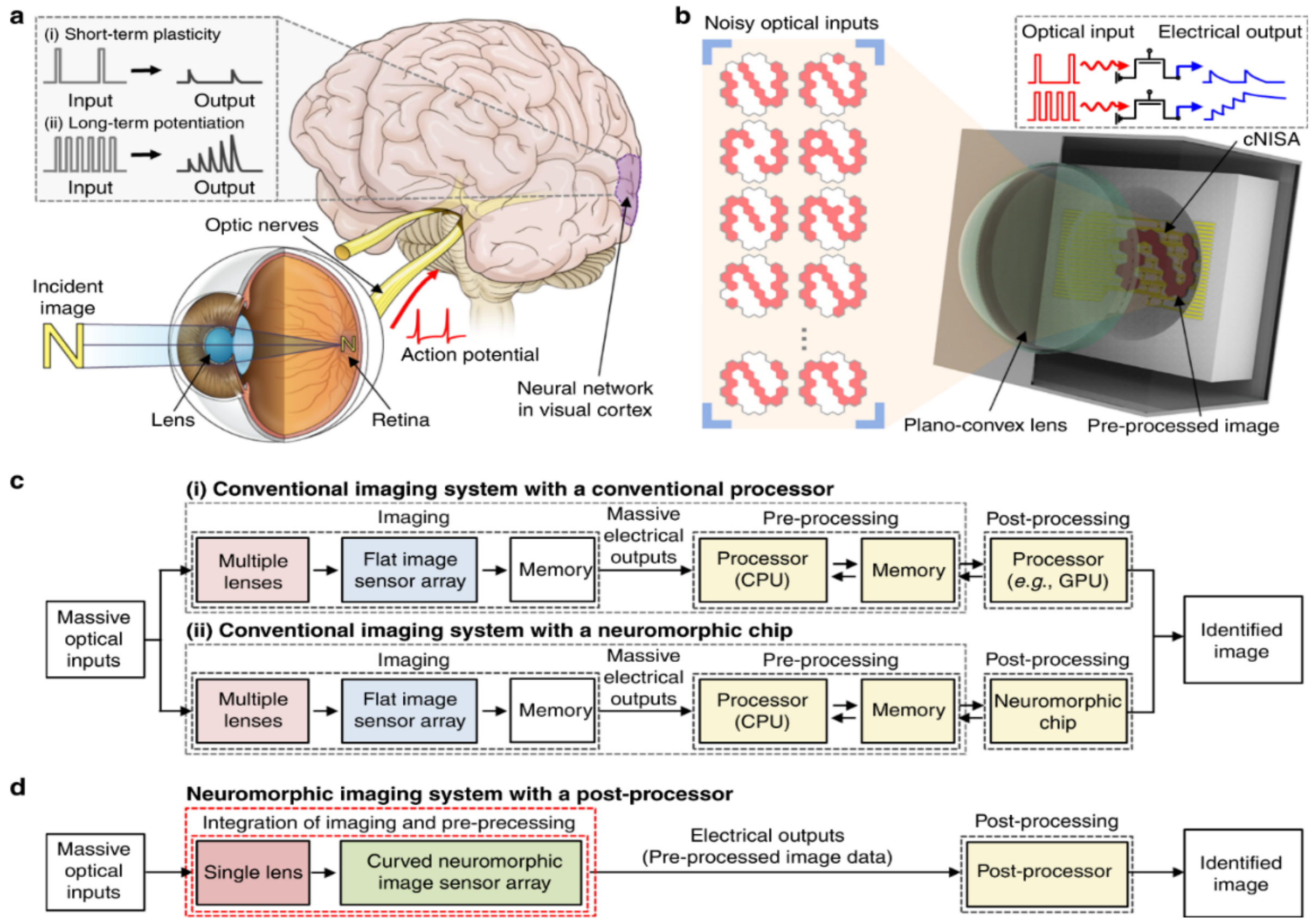
- Choi, C.; Leem, J.; Kim, M.S.; Taqieddin, A.; Cho, C.; Cho, K.W.; Lee, G.J.; Seung, H.; Bae, H.J.; Song, Y.M.; et al. Curved Neuromorphic Image Sensor Array Using a MoS2-Organic Heterostructure Inspired by the Human Visual Recognition System. Nat. Commun. 2020, 11, 5934. [Google Scholar] [CrossRef]
- Liu, Y.; Peng, J.; Wang, S.; Xu, M.; Gao, M.; Xia, T.; Weng, J.; Xu, A.; Liu, S. Molybdenum Disulfide/Graphene Oxide Nanocomposites Show Favorable Lung Targeting and Enhanced Drug Loading/Tumor-Killing Efficacy with Improved Biocompatibility. NPG Asia Mater. 2018, 10, e458. [Google Scholar] [CrossRef] [Green Version]
- Zheng, C.; Jin, X.; Li, Y.; Mei, J.; Sun, Y.; Xiao, M.; Zhang, H.; Zhang, Z.; Zhang, G.-J. Sensitive Molybdenum Disulfide Based Field Effect Transistor Sensor for Real-Time Monitoring of Hydrogen Peroxide. Sci. Rep. 2019, 9, 759. [Google Scholar] [CrossRef]
- Ding, X.; Peng, F.; Zhou, J.; Gong, W.; Slaven, G.; Loh, K.P.; Lim, C.T.; Leong, D.T. Defect Engineered Bioactive Transition Metals Dichalcogenides Quantum Dots. Nat. Commun. 2019, 10, 41. [Google Scholar] [CrossRef]
- Faramarzi, V.; Ahmadi, V.; Fotouhi, B.; Abasifard, M. A Potential Sensing Mechanism for DNA Nucleobases by Optical Properties of GO and MoS2 Nanopores. Sci. Rep. 2019, 9, 6230. [Google Scholar] [CrossRef] [Green Version]
- Singh, C.; Ali, M.A.; Kumar, V.; Ahmad, R.; Sumana, G. Functionalized MoS2 Nanosheets Assembled Microfluidic Immunosensor for Highly Sensitive Detection of Food Pathogen. Sens. Actuators B Chem. 2018, 259, 1090–1098. [Google Scholar] [CrossRef]
- Barati Farimani, A.; Heiranian, M.; Aluru, N.R. Identification of Amino Acids with Sensitive Nanoporous MoS2: Towards Machine Learning-Based Prediction. NPJ 2D Mater. Appl. 2018, 2, 14. [Google Scholar] [CrossRef]
- Shi, T.; Hou, X.; Guo, S.; Zhang, L.; Wei, C.; Peng, T.; Hu, X. Nanohole-Boosted Electron Transport between Nanomaterials and Bacteria as a Concept for Nano–Bio Interactions. Nat. Commun. 2021, 12, 493. [Google Scholar] [CrossRef]
- Zhang, W.; Zhang, P.; Su, Z.; Wei, G. Synthesis and Sensor Applications of MoS2 -Based Nanocomposites. Nanoscale 2015, 7, 18364–18378. [Google Scholar] [CrossRef]
- Concept for Two-Dimensional TMDs as Functional Layer for Gas Sensing Applications|VDE Conference Publication|IEEE Xplore. Available online: https://ieeexplore.ieee.org/document/9257305 (accessed on 14 March 2021).
- Scalable Growth of High-Quality MoS2 Film by Magnetron Sputtering: Application for NO2 Gas Sensing|IEEE Conference Publication|IEEE Xplore. Available online: https://ieeexplore.ieee.org/document/9033716 (accessed on 14 March 2021).
- Thin EOT MoS2 FET for Efficient Photodetection and Gas Sensing|IEEE Conference Publication|IEEE Xplore. Available online: https://ieeexplore.ieee.org/document/8937927 (accessed on 14 March 2021).
- Multilayer CVD-Graphene and MoS₂ Ethanol Sensing and Characterization Using Kretschmann-Based SPR|IEEE Journals & Magazine|IEEE Xplore. Available online: https://ieeexplore.ieee.org/document/9187269 (accessed on 14 March 2021).
- Huang, Y.; Shi, Y.; Yang, H.Y.; Ai, Y. A Novel Single-Layered MoS2 Nanosheet Based Microfluidic Biosensor for Ultrasensitive Detection of DNA. Nanoscale 2015, 7, 2245–2249. [Google Scholar] [CrossRef]
- Surface Plasmon Resonance (SPR) for Sensors and Biosensors-ScienceDirect. Available online: https://www.sciencedirect.com/science/article/pii/B9780323497787000060 (accessed on 13 March 2021).
- Rahman, M.M.; Rahman, M.S.; Rikta, K.A.; Rana, M.M.; Anower, M.S.; Paul, A.K. Promising SPR Biosensors Applying 2D Materials with α-SnSe Allotrope for Sensing Applications. In Proceedings of the 2020 IEEE Region 10 Symposium (TENSYMP); IEEE: Dhaka, Bangladesh, 2020; pp. 1197–1200. [Google Scholar]
- Tan, Y.; He, R.; Cheng, C.; Wang, D.; Chen, Y.; Chen, F. Polarization-Dependent Optical Absorption of MoS2 for Refractive Index Sensing. Sci Rep 2015, 4, 7523. [Google Scholar] [CrossRef] [Green Version]
- Mukherjee, B.; Kaushik, N.; Tripathi, R.P.N.; Joseph, A.M.; Mohapatra, P.K.; Dhar, S.; Singh, B.P.; Kumar, G.V.P.; Simsek, E.; Lodha, S. Exciton Emission Intensity Modulation of Monolayer MoS2 via Au Plasmon Coupling. Sci. Rep. 2017, 7, 41175. [Google Scholar] [CrossRef]
- Chen, C.H.; Chang, X.; Wu, C.S. A novel shaped-controlled fabrication of nanopore and its applications in quantum electronics. Sci. Rep. 2019, 9, 18663. [Google Scholar] [CrossRef]
- Pham, T.; Li, G.; Bekyarova, E.; Itkis, M.E.; Mulchandani, A. MoS2-Based Optoelectronic Gas Sensor with Sub-Parts-per-Billion Limit of NO2 Gas Detection. ACS Nano 2019, 13, 3196–3205. [Google Scholar] [CrossRef]
- Kinnamon, D.; Ghanta, R.; Lin, K.-C.; Muthukumar, S.; Prasad, S. Portable Biosensor for Monitoring Cortisol in Low-Volume Perspired Human Sweat. Sci. Rep. 2017, 7, 13312. [Google Scholar] [CrossRef] [Green Version]
- Hwang, J.C.M. Novel Materials and Devices for Millimeter-Wave and THz Applications. In Proceedings of the 2012 IEEE MTT-S International Microwave Workshop Series on Millimeter Wave Wireless Technology and Applications, Nanjing, China, 18–20 September 2012; IEEE: Nanjing, China, 2012; p. 1. [Google Scholar]
- Jung, Y.H.; Seo, J.-H.; Zhang, H.; Lee, J.; Cho, S.J.; Chang, T.-H.; Ma, Z. Radio-Frequency Flexible and Stretchable Electronics: The Need, Challenges and Opportunities. In Proceedings of the Micro- and Nanotechnology Sensors, Systems, and Applications IX, SPIE Defense + Security, International Society for Optics and Photonics. Anaheim, CA, USA, 18 May 2017; Volume 10194, p. 101941C. [Google Scholar] [CrossRef]
- Dejband, E.; Karami, H.; Hosseini, M.; Torkaman, P. Switchable Abnormal THz Wave Reflector Based on Molybdenum Disulfide (MoS2). In Proceedings of the 2018 Fifth International Conference on Millimeter-Wave and Terahertz Technologies (MMWaTT), Tehran, Iran, 18–20 December 2018; IEEE: Tehran, Iran, 2018; pp. 58–61. [Google Scholar]
- Hijazi, A.; Moutaouakil, A.E. Graphene and MoS2 Structures for THz Applications. In Proceedings of the 2019 44th International Conference on Infrared, Millimeter, and Terahertz Waves (IRMMW-THz), Paris, France, 1–6 September 2019; IEEE: Paris, France, 2019; pp. 1–2. [Google Scholar]
- Moutaouakil, A.E.; Komori, T.; Horiike, K.; Suemitsu, T.; Otsuji, T. Room Temperature Intense Terahertz Emission from a Dual Grating Gate Plasmon-Resonant Emitter Using InAlAs/InGaAs/InP Material Systems. IEICE Trans. Electron. 2010, E93.C, 1286–1289. [Google Scholar] [CrossRef]
- Moutaouakil, A.E. Two-Dimensional Electronic Materials for Terahertz Applications: Linking the Physical Properties with Engineering Expertise. In Proceedings of the 2018 6th International Renewable and Sustainable Energy Conference (IRSEC), Rabat, Morocco, 5–8 December 2018; pp. 1–4. [Google Scholar]
- Moutaouakil, A.E.; Suemitsu, T.; Otsuji, T.; Coquillat, D.; Knap, W. Nonresonant Detection of Terahertz Radiation in High-Electron-Mobility Transistor Structure Using InAlAs/InGaAs/InP Material Systems at Room Temperature. J. Nanosci. Nanotechnol. 2012, 12, 6737–6740. [Google Scholar] [CrossRef]
- Moutaouakil, A.E.; Suemitsu, T.; Otsuji, T.; Coquillat, D.; Knap, W. Room Temperature Terahertz Detection in High-Electron-Mobility Transistor Structure Using InAlAs/InGaAs/InP Material Systems. In Proceedings of the 35th International Conference on Infrared, Millimeter, and Terahertz Waves, Rome, Italy, 5–10 September 2010; IEEE: Rome, Italy, 2010; pp. 1–2. [Google Scholar]
- Moutaouakil, A.E.; Watanabe, T.; Haibo, C.; Komori, T.; Nishimura, T.; Suemitsu, T.; Otsuji, T. Spectral Narrowing of Terahertz Emission from Super-Grating Dual-Gate Plasmon-Resonant High-Electron Mobility Transistors. J. Phys. Conf. Ser. 2009, 193, 012068. [Google Scholar] [CrossRef]
- El Moutaouakil, A.; Suemitsu, T.; Otsuji, T.; Videlier, H.; Boubanga-Tombet, S.-A.; Coquillat, D.; Knap, W. Device Loading Effect on Nonresonant Detection of Terahertz Radiation in Dual Grating Gate Plasmon-Resonant Structure Using InGaP/InGaAs/GaAs Material Systems. Phys. Status Solidi (C) 2011, 8, 346–348. [Google Scholar] [CrossRef]
- Cao, Y.; Gan, S.; Geng, Z.; Liu, J.; Yang, Y.; Bao, Q.; Chen, H. Optically Tuned Terahertz Modulator Based on Annealed Multilayer MoS2. Sci. Rep. 2016, 6, 22899. [Google Scholar] [CrossRef]
- Goel, N.; Bera, J.; Kumar, R.; Sahu, S.; Kumara, M. MoS2-PVP Nanocomposites Decorated ZnO Microsheets for Efficient Hydrogen Detection. IEEE Sens. J. 2021, 1. [Google Scholar] [CrossRef]
- Tran, P.D.; Tran, T.V.; Orio, M.; Torelli, S.; Truong, Q.D.; Nayuki, K.; Sasaki, Y.; Chiam, S.Y.; Yi, R.; Honma, I.; et al. Coordination Polymer Structure and Revisited Hydrogen Evolution Catalytic Mechanism for Amorphous Molybdenum Sulfide. Nat. Mater. 2016, 15, 640–646. [Google Scholar] [CrossRef] [PubMed]
- Balat, M. Potential Importance of Hydrogen as a Future Solution to Environmental and Transportation Problems. Int. J. Hydrog. Energy 2008, 33, 4013–4029. [Google Scholar] [CrossRef]
- Gao, M.-R.; Chan, M.K.Y.; Sun, Y. Edge-Terminated Molybdenum Disulfide with a 9.4-Å Interlayer Spacing for Electrochemical Hydrogen Production. Nat. Commun. 2015, 6, 7493. [Google Scholar] [CrossRef] [Green Version]
- Saha, D.; Kruse, P. Editors’ Choice—Review—Conductive Forms of MoS2 and Their Applications in Energy Storage and Conversion. J. Electrochem. Soc. 2020, 167, 126517. [Google Scholar] [CrossRef]
- Wang, Z.; Mi, B. Environmental Applications of 2D Molybdenum Disulfide (MoS2) Nanosheets. Environ. Sci. Technol. 2017, 51, 8229–8244. [Google Scholar] [CrossRef]
- Gao, X.; Wang, X.; Ouyang, X.; Wen, C. Flexible Superhydrophobic and Superoleophilic MoS2 Sponge for Highly Efficient Oil-Water Separation. Sci. Rep. 2016, 6, 27207. [Google Scholar] [CrossRef] [Green Version]
- Dey, M.; Dey, M.; Alam, S.; Das, N.K.; Matin, M.A.; Amin, N. Study of Molybdenum Sulphide as a Novel Buffer Layer for CZTS Solar Cells. In Proceedings of the 2016 3rd International Conference on Electrical Engineering and Information Communication Technology (ICEEICT), Dhaka, Bangladesh, 22–24 September 2016; IEEE: Dhaka, Bangladesh, 2016; pp. 1–4. [Google Scholar]
- Iqbal, M.Z.; Nabi, J.; Siddique, S.; Awan, H.T.A.; Haider, S.S.; Sulman, M. Role of Graphene and Transition Metal Dichalcogenides as Hole Transport Layer and Counter Electrode in Solar Cells. Int. J. Energy Res. 2020, 44, 1464–1487. [Google Scholar] [CrossRef]
- Capasso, A.; Del Rio Castillo, A.E.; Najafi, L.; Pellegrini, V.; Bonaccorso, F.; Matteocci, F.; Cina, L.; Di Carlo, A. Spray Deposition of Exfoliated MoS2 Flakes as Hole Transport Layer in Perovskite-Based Photovoltaics. In Proceedings of the 2015 IEEE 15th International Conference on Nanotechnology (IEEE-NANO), Rome, Italy, 27–30 July 2015; IEEE: Rome, Italy, 2015; pp. 1138–1141. [Google Scholar]
- Xu, H.; Xin, L.; Liu, L.; Pang, D.; Jiao, Y.; Cong, R.; Yu, W. Large Area MoS2/Si Heterojunction-Based Solar Cell through Sol-Gel Method. Mater. Lett. 2019, 238, 13–16. [Google Scholar] [CrossRef]
- Liang, M.; Ali, A.; Belaidi, A.; Hossain, M.I.; Ronan, O.; Downing, C.; Tabet, N.; Sanvito, S.; EI-Mellouhi, F.; Nicolosi, V. Improving Stability of Organometallic-Halide Perovskite Solar Cells Using Exfoliation Two-Dimensional Molybdenum Chalcogenides. NPJ 2D Mater. Appl. 2020, 4, 40. [Google Scholar] [CrossRef]
- Huang, Y.; Wang, Y.; Zhang, X.; Lai, F.; Sun, Y.; Li, Q.; Wang, H. N-Doped Carbon@nanoplate-Assembled MoS2 Hierarchical Microspheres as Anode Material for Lithium-Ion Batteries. Mater. Lett. 2019, 243, 84–87. [Google Scholar] [CrossRef]
- Bao, W.; Cai, X.; Kim, D.; Sridhara, K.; Fuhrer, M.S. High Mobility Ambipolar MoS2 Field-Effect Transistors: Substrate and Dielectric Effects. Appl. Phys. Lett. 2013, 102, 042104. [Google Scholar] [CrossRef] [Green Version]
- Kramer, A.; Van de Put, M.L.; Hinkle, C.L.; Vandenberghe, W.G. Tellurium as a Successor of Silicon for Extremely Scaled Nanowires: A First-Principles Study. NPJ 2D Mater. Appl. 2020, 4, 10. [Google Scholar] [CrossRef]
- Manzeli, S.; Ovchinnikov, D.; Pasquier, D.; Yazyev, O.V.; Kis, A. 2D Transition Metal Dichalcogenides. Nat. Rev. Mater 2017, 2, 17033. [Google Scholar] [CrossRef]
- Cao, W.; Kang, J.; Sarkar, D.; Liu, W.; Banerjee, K. 2D Semiconductor FETs—Projections and Design for Sub-10 Nm VLSI. IEEE Trans. Electron Devices 2015, 62, 3459–3469. [Google Scholar] [CrossRef]
- Wang, H.; Li, C.; Fang, P.; Zhang, Z.; Zhang, J.Z. Synthesis, Properties, and Optoelectronic Applications of Two-Dimensional MoS2 and MoS2-Based Heterostructures. Chem. Soc. Rev. 2018, 47, 6101–6127. [Google Scholar] [CrossRef]
- Stroud, A.; Derosa, P.A.; Leuty, G.; Muratore, C.; Berry, R.; Muratory, C. Effects of Impurities and Lattice Imperfections on the Conductive Properties of MoS2. In Proceedings of the 2015 IEEE 15th International Conference on Nanotechnology (IEEE-NANO), Rome, Italy, 27–30 July 2015; IEEE: Rome, Italy, 2015; pp. 613–616. [Google Scholar]
- Yu, S.; Wu, X.; Wang, Y.; Guo, X.; Tong, L. 2D Materials for Optical Modulation: Challenges and Opportunities. Adv. Mater. 2017, 29, 1606128. [Google Scholar] [CrossRef]
- Chen, X.; Shinde, S.M.; Dhakal, K.P.; Lee, S.W.; Kim, H.; Lee, Z.; Ahn, J.-H. Degradation Behaviors and Mechanisms of MoS2 Crystals Relevant to Bioabsorbable Electronics. NPG Asia Mater. 2018, 10, 810–820. [Google Scholar] [CrossRef] [Green Version]
- Shree, S.; Paradisanos, I.; Marie, X.; Robert, C.; Urbaszek, B. Guide to Optical Spectroscopy of Layered Semiconductors. Nat. Rev. Phys. 2021, 3, 39–54. [Google Scholar] [CrossRef]
- Peng, Z.; Chen, X.; Fan, Y.; Srolovitz, D.J.; Lei, D. Strain Engineering of 2D Semiconductors and Graphene: From Strain Fields to Band-Structure Tuning and Photonic Applications. Light. Sci. Appl. 2020, 9, 190. [Google Scholar] [CrossRef]
- Fan, X.; Zheng, W.T.; Kuo, J.-L.; Singh, D.J. Structural Stability of Single-Layer MoS2 under Large Strain. J. Phys. Condens. Matter 2015, 27, 105401. [Google Scholar] [CrossRef]
- Kumar, P.; Horwath, J.P.; Foucher, A.C.; Price, C.C.; Acero, N.; Shenoy, V.B.; Stach, E.A.; Jariwala, D. Direct Visualization of Out-of-Equilibrium Structural Transformations in Atomically Thin Chalcogenides. NPJ 2D Mater. Appl. 2020, 4, 16. [Google Scholar] [CrossRef]
- Kaur, J.; Singh, M.; Dell‘Aversana, C.; Benedetti, R.; Giardina, P.; Rossi, M.; Valadan, M.; Vergara, A.; Cutarelli, A.; Montone, A.M.I.; et al. Biological Interactions of Biocompatible and Water-Dispersed MoS2 Nanosheets with Bacteria and Human Cells. Sci. Rep. 2018, 8, 16386. [Google Scholar] [CrossRef]
- Wu, B.; Chen, L.; Wu, X.; Hou, H.; Wang, Z.; Liu, S. Differential Influence of Molybdenum Disulfide at the Nanometer and Micron Scales in the Intestinal Metabolome and Microbiome of Mice. Environ. Sci. Nano 2019, 6, 1594–1606. [Google Scholar] [CrossRef]


| 1T | 2H | 3R | |
|---|---|---|---|
| Structure Coordination | Octahedral | Trigonal Prismatic | Trigonal Prismatic |
| Lattice parameters | a = 5.60 A, c = 5.99 A and an edge sharing octahedral [34] | a = 3.15 A, c = 12.30 A [34] | a = 3.17 Å, c = 18.38 A [34] |
| property | paramagnetic and metallic | Semiconducting | |
| Electrical conductivity | 105 times higher than 2H phase | Low (~0.1 S/m) | |
| Absorption peaks | No peaks at 604 nm and 667 nm | Showed peaks at 604 nm and 667 nm | |
| Common applications | Intercalation in chemistry | Dry lubricants | Dry lubricants and non-linear optical devices |
| Bulk | Monolayer | |
|---|---|---|
| Bandgap | Indirect (~1.2 eV) | Direct (1.8 eV) |
| Binding energy | 0.1 eV | 1.1 eV |
| Photoluminescence intensities | between 10−5 and 10−6 | 104 times higher than that of bulk, up to and up to 4 × 10⁻³ |
| Technique | Charecteristics of the Obtained MoS2 Sheets | Publisher | Year | Reference |
|---|---|---|---|---|
| Using aerogel | A rapid synthesis technique for TMDs- carbon aerogel composites to be used in supercapacitor. The preparation time is 30 min which is approximately 2% of typical aerogel techniques that take 24 h | Nature | 2017 | [58] |
| Liquid assisted Sonication | Studied the PL, Raman analysis resulting from bath and probe sonication synthesis | Elsevier | 2020 | [59] |
| Liquid exfoliation & ultrasonic cavitation | Obtain less defective and high concentration nanosheets in a short time | Nature | 2014 | [60] |
| Exfoliation of & Ultrasound Sonication in Supercritical Co2 | Exfoliation efficiency > 90% | Springer | 2019 | [61] |
| Exfoliation & sonication | Mobility = 10 cm2/V, on/off ratios = 106 | Nature | 2018 | [69] |
| ALD & thermal evaporation | Enhanced electrical conductivity | Nature | 2016 | [66] |
| CVD & liquid precursor | The method uses water to remove impurities like carbon and sulphur. It ensures full coverage of MoS2 for the substrate | Nature | 2017 | [65] |
| ALD & thermal evaporation | The carrier density and conductivity of MoS2 are adjusted according to the thickness of the metalloporphyrin layer used. Produce large scale MoS2 nanosheets | Nature | 2016 | [66] |
| Self propagation of Mo poweder and elementary Sulfur | Resulted MoS2 nanosheets have thermal stability up to 400 °C. | IEEE | 2013 | [18] |
| CVD with Sulfur as a precursor (Sulfidation) | on/off current ratio of 105, a mobility of 0.12 cm2/V·s (mean mobility value of 0.07 cm2 /V·s | Royal society of chemistry | 2014 | [67] |
| Sulfidation | The on/off ratio of 103–104 and electron mobility of 10−4 cm2/V·s | Elsevier | 2020 | [68] |
| Intercalation & exfoliation | To be used in high-performance thin-film transistors, on/off ratio of 106 and electron mobility of 10 cm2/V·s | Springer Nature | 2018 | [69] |
| Categeory | Application | MoS2 Property | Reference |
|---|---|---|---|
| Optoelectronics | Photosensing (photodetector) | Electronic and optical properties | [72] |
| Photosensing (photodetector) | [73] | ||
| Photosensing (photodetector) | [74] | ||
| Recognition systems and IoT | Image sensors | Optical properties | [84] |
| Medical (bio-sensing) | Cancer sensing | PL property | [86] |
| Cancer sensing | PL property | [23] | |
| Cancer sensing | PL property | [21] | |
| DNA sensing | MoS2 nanopores | [88] | |
| DNA sensing | dye quenching property | [97] | |
| Amino acids sensing | MoS2 nanopores | [90] | |
| Immunosensors | Electrochemical and optical properties | [89] |
| Application | Categeory | Description | Publisher | Year | Reference |
|---|---|---|---|---|---|
| Electronics | Analogue | Developing a 2D MoS2 field-effect transistors (FETs) to be used as operational amplifier | Nature | 2020 | [71] |
| Electronics | CMOS | Enhanced back gate MoS2 FETs using Sulfur treatment, gate length from 500 to 80 nm, contact resistance = 1.3 kΩ | IEEE | 2020 | [75] |
| Electronics | nonvolatile memoryNVM | Hystresses and capacitance of MoS2 NVM with 9nm and 15 nm blocking oxide layer of SiO2 is investigated. The device has largest hystresses window. And can store both electrons and holes | IEEE | 2016 | [77] |
| Electronics | Power electronics | Ultra low power transistor of SS ~4.5 mm/decade and steep on/off characteristics | Nature | 2020 | [76] |
| Electronics | optoelectronics | Developing a highly-efficient and fast photodetector using amorphous silicon and MoS2 | Nature | 2013 | [72] |
| Electronics | optoelectronics | Efficient photodetector with photocurrent gain of 1.6, specific detectivity of 4.32 × 10⁸ Jones and quantum efficiency ~1.0 × 10¹⁰ at 365 nm | Nature | 2020 | [73] |
| Electronics | optoelectronics | A nanoscale photodetector, energy efficient (consumes from 1 to 1000 nanojoules), and has a small fingerprint of (~1 μm × 5 μm). | Nature | 2020 | [74] |
| Electronics | Image sensors | A MoS2-organic heterostructure image sensor similar to human vision system using simple design. The output has less noise and without redundant input data | Nature | 2020 | [84] |
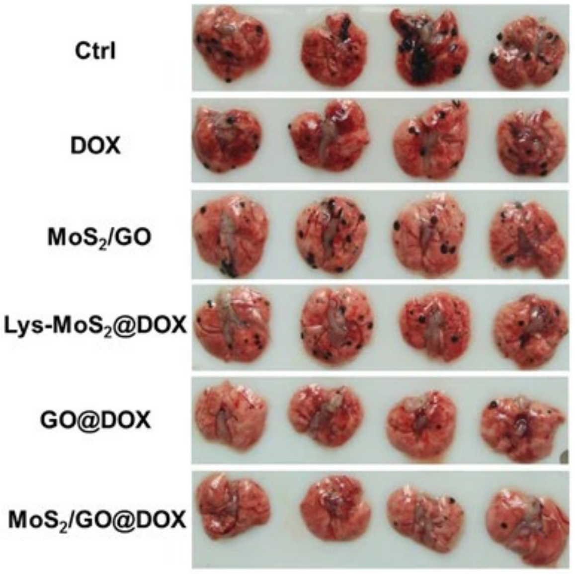
| Medical | Cancer cure | Using MoS2/GO nanocomposites to cure lung cancer in mice | Nature | 2018 | [85] |
| Medical | Cancer cure | Using defect engineering (Sulfur defects) in MoS2 quantum dots to kill cancer cells. The Sulfur defects increased oxidation strees and was able to inhibit cancer growth cells | Nature | 2019 | [87] |
| Medical | Cancer detecction | A real-time MoS2 FET sensor to detect H2O2 in biological cells | Nature | 2019 | [86] |
| Medical | Cancer detecction | MoS2 nanosheet fluorescent biosensor for detecting prostate antigen. A 20 μg/mL of MoS2 nanosheets quenched up to 97% of the dye | Springer | 2014 | [23] |
| Medical | Cancer detecction | Detecting breast cancer based on PL property of MoS2. A redshift of 16 nm takes place for miRNA21c (a cancer biomarker) | Nature | 2020 | [21] |
| Medical | DNA detection | Sensing DNA nucleobases using MoS2 nanopores. Molar absorption of MoS2 nanopore of 0.65 nm thick, and lengths 2 nm, 3 nm, 5 nm. | Nature | 2019 | [88] |
| Medical | DNA detection | Detecting DNA based on dye quenching property of MoS2. The device has linear range (0 to 50 nM), and a detection limit = 500 pM | Royal Scociety of chemistry | 2015 | [97] |
| Medical | Amino acid detection | Using MoS2 nanopores and machine learning to detect ionic current and residence time of 20 different amino acids with accuracy range 72.45% to 99.6% | Nature | 2018 | [90] |
| Medical | Microfluidic immunosensor | Use of MoS2 nanosheets on microfluidic electrodes to detect Salmonella typhimurium (S.typhimurium) sensitivity = 1.79 kΩ/(CFU/mL.cm2) detection limit = 1.56 CFU/mL detection range = 10–107 CFU/mL. | Elsevier | 2017 | [89] |
| Medical | Antibacterial materials | Using nanohole enriched MoS2 to destroy bacteria. MoS2 concentration used is 4 μg/mL. It has affinity response with biofilms of 14.71 nM, 1.3-fold > 11.44 nM obtained for pristine MoS2 Verified in vitro and viro | Nature | 2021 | [91] |
| Energy | Solar cells | Using MoS2 as a buffer in solar cells to enhance efficiency and stability | IEEE | 2016 | [123] |
| Energy | Solar cells | Using MoS2 as a hole transport layer in solar cells a peak at 404 cm−1, at 200 °C, and two more peaks at at 380 and 404 cm−1, at 300 °C, | Wiley | 2019 | [124] |
| Energy | Solar cells | MoS2 as a transport layer in perovskite solar cells PCE (η) = 3.9% compared to other cells of (η = 3.1%). High stability for 800-hour shelf life (ΔPCE/PCE = −17%) when compared to other cells of (ΔPCE/PCE = −45%). | IEEE | 2015 | [125] |
| Energy | Solar cells | Using MoS2/Si heterojunction in solar cells to enhance conversion efficiency from 1.1% to 4.6%. | Elsevier | 2018 | [126] |
| Energy | Solar cells | Enhancing organometallic-halide perovskite solar using MoS2 as a buffer Cells (PCE) = 14.9%, and maintaing 93.1% of its PCE after 1 hour | Nature | 2020 | [127] |
| Energy | lithium-ion batteries | Using MoS2 as as anode material for lithium-ion batteries.It has capacity of 1103.6 mAh/g and maintains a reversible capacity of 786.4 mAh/g after 50 cycles at 0.1 A/g | Elsevier | 2019 | [128] |
| THz applications | THz wave reflector | Switchable THz wave reflector made of MoS2, SiO2, and gold layers. reflection phase ranges from 0 to 2π linear phase shift according to the geometric dimension | IEEE | 2018 | [107] |
| THz applications | THz modulator | Terahertz modulator of multilayer-MoS2 on Silicon (MOS). Moudulation efficiency of annealed MOS is higher that that of graphene over Silicon and graphene metamaterials | Nature | 2016 | [115] |
| Other | Hydrogen detection | MoS2-PVP (Polyvinyl pyridine) nanocomposite with ZnO to detect hydrogen. A 5 mg/mL sensor has 8 times better ensing than pristine ZnO | IEEE | 2021 | [116] |
| Other | Hydrogen generation | coordination polymer based on [Mo3S13]2− clusters from amorphous MoS2 to be used in hydrogen evolution reactions. | Nature | 2016 | [117] |
| Other | Hydrogen generation | A edge-terminated and interlayer-expanded MoS2 catalyst fabricated using a microwave heating strategy. The proposed structure has the highest hydrogen evolution activity and best stability | Nature | 2015 | [118] |
| Other | Oil separation from water | MoS2 Sponge to absorb oil from water. Simple fabrication and easy scaling up. | Nature | 2016 | [122] |
| Challenge | Description | Publisher | Year | Reference |
|---|---|---|---|---|
| Properties | Effect of lattice imperfections and atomic vacancies on density of states and electron-hole transport | IEEE | 2015 | [134] |
| Properties | Degradation behavior of MoS2 crystals | NPG Asia Materials | 2018 | [136] |
| Properties | structural transformations in MoS2 thin layers under high temperature | Nature | 2020 | [140] |
| Electronics | Sub 10 nm FETs challenges and Strain effects | IEEE | 2015 | [132] |
| Optoelectronics | Optical modulation challenges and laser damage | Advanced Materials | 2017 | [135] |
| Optoelectronics | optical spectroscopy for MoS2 layers, the absorption and emission behavior and how to tune them | Nature | 2021 | [137] |
| Optoelectronics | Strain engineering to develop optical properties and using it in photonics applications | Nature | 2020 | [138] |
| Optoelectronics | Failure mechanisms of monolayer MoS2 under large strain | Journal of physics | 2015 | [139] |
| Biomedical (biocompatibility) | Cytotoxic effect of MoS2 when used to cure cancer cells | Nature | 2018 | [141] |
| Biomedical (biocompatibility) | Effect of nano-MoS2 on mice intestine where it caused intestinal inflation and changes in the metabolism and the microbiota | Royal Society of chemistry | 2019 | [142] |
Publisher’s Note: MDPI stays neutral with regard to jurisdictional claims in published maps and institutional affiliations. |
© 2021 by the authors. Licensee MDPI, Basel, Switzerland. This article is an open access article distributed under the terms and conditions of the Creative Commons Attribution (CC BY) license (http://creativecommons.org/licenses/by/4.0/).
Share and Cite
Samy, O.; Zeng, S.; Birowosuto, M.D.; El Moutaouakil, A. A Review on MoS2 Properties, Synthesis, Sensing Applications and Challenges. Crystals 2021, 11, 355. https://doi.org/10.3390/cryst11040355
Samy O, Zeng S, Birowosuto MD, El Moutaouakil A. A Review on MoS2 Properties, Synthesis, Sensing Applications and Challenges. Crystals. 2021; 11(4):355. https://doi.org/10.3390/cryst11040355
Chicago/Turabian StyleSamy, Omnia, Shuwen Zeng, Muhammad Danang Birowosuto, and Amine El Moutaouakil. 2021. "A Review on MoS2 Properties, Synthesis, Sensing Applications and Challenges" Crystals 11, no. 4: 355. https://doi.org/10.3390/cryst11040355