Next Issue
Volume 10, January
Previous Issue
Volume 9, November


Micromachines, Volume 9, Issue 12 (December 2018) – 72 articles

Cover Story (view full-size image): 
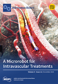
A particular challenge in intravascular treatments is the control of submillimeter guidewires. This requires a new microrobotics approach. A soft magnetic microrobot is required, consisting of (1) a flexible polydimethylsiloxane (PDMS) body, (2) two permanent magnets, and (3) a micro-spring connector designed and controlled in any 2D arbitrary paths. The proposed soft microrobot has the potential to improve guidewire control in a percutaneous coronary intervention (PCI) phantom. View this paper.
  • Issues are regarded as officially published after their release is announced to the table of contents alert mailing list.
  • You may sign up for e-mail alerts to receive table of contents of newly released issues.
  • PDF is the official format for papers published in both, html and pdf forms. To view the papers in pdf format, click on the "PDF Full-text" link, and use the free Adobe Reader to open them.
Order results
Result details
Section
Select all
Export citation of selected articles as:
13 pages, 4377 KiB  
Article
Integration Method of Microchannel and Vertical Micromesh Structure for Three-Dimensional Cell Culture Using Inclined Exposure and Inclined Oxygen Ashing
by Hidetaka Ueno, Kou Yamada and Takaaki Suzuki
Micromachines 2018, 9(12), 681; https://doi.org/10.3390/mi9120681 - 19 Dec 2018
Cited by 5 | Viewed by 3473
Abstract
Culturing cellular tissues inside a microchannel using an artificial three-dimensional (3D) microstructure is normally conducted to elucidate and reproduce a biological function. The thick photoresist SU-8, which has a microscale resolution and high aspect ratio, is widely used for the fabrication of microchannels [...] Read more.
Culturing cellular tissues inside a microchannel using an artificial three-dimensional (3D) microstructure is normally conducted to elucidate and reproduce a biological function. The thick photoresist SU-8, which has a microscale resolution and high aspect ratio, is widely used for the fabrication of microchannels and scaffolds having 3D structures for cell culture. However, it is difficult to accurately fabricate a mesh structure with a pore size that is smaller than the cells that has an overall height greater than 50 μm because of the deterioration of the verticality of exposure light and the diffusion of acid, which accelerates the crosslinking reaction in the SU-8 layer. In this study, we propose a method of integrating a vertical porous membrane into a microchannel. The resolution of the vertical porous membrane becomes more accurate through inclined oxygen ashing, without degrading the robustness. Because a single mask pattern is required for the proposed method, assembly error is not generated using the assembly-free process. The fabricated vertical porous membrane in the microchannel contained micropores that were smaller than the cells and sufficiently robust for a microfluidic system. HepG2 cells were attached three-dimensionally on the fabricated vertical porous membrane to demonstrate 3D cell culture. Full article
(This article belongs to the Special Issue SU-8 for Microfluidics and Lab-on-a-chip)
Show Figures

Figure 1

11 pages, 4226 KiB  
Article
Demulsification of Kerosene/Water Emulsion in the Transparent Asymmetric Plate-Type Micro-Channel
by Da Ruan, Diliyaer Hamiti, Zheng-Dong Ma, Ya-Dong Pu and Xiao Chen
Micromachines 2018, 9(12), 680; https://doi.org/10.3390/mi9120680 - 19 Dec 2018
Cited by 4 | Viewed by 3161
Abstract
Asymmetric plate-type micro-channels (APM) have one hydrophobic wall and one hydrophilic wall. By flowing through APM, a kerosene-in-water emulsion can be de-emulsified in one second. To date, however, the demulsification process in the APM is still a black box. In order to observe [...] Read more.
Asymmetric plate-type micro-channels (APM) have one hydrophobic wall and one hydrophilic wall. By flowing through APM, a kerosene-in-water emulsion can be de-emulsified in one second. To date, however, the demulsification process in the APM is still a black box. In order to observe the demulsification process directly, transparent asymmetric plate-type micro-channels (TAPM) were fabricated with two surface-modified glass plates. Emulsions with oil contents of 10%, 30%, and 50% were pumped through TAPM with heights of 39.2 μm and 159.5 μm. The movement and coalescence of oil droplets (the dispersed phase of a kerosene-in-water emulsion) in the TAPM were observed directly with an optical microscope. By analyzing videos and photographs, it was found that the demulsification process included three steps: oil droplets flowed against and were adsorbed on the hydrophobic wall, then oil droplets coalesced to form larger droplets, whereupon the oil phase was separated. The experimental results showed that the demulsification efficiency was approximately proportional to the oil content (30–50%) of the emulsions and increased when the micro-channel height was reduced. Full article
(This article belongs to the Section B:Biology and Biomedicine)
Show Figures

Figure 1

19 pages, 3134 KiB  
Review
Nanowire-Based Biosensors: From Growth to Applications
by Pranav Ambhorkar, Zongjie Wang , Hyuongho Ko, Sangmin Lee, Kyo-in Koo, Keekyoung Kim and Dong-il (Dan) Cho
Micromachines 2018, 9(12), 679; https://doi.org/10.3390/mi9120679 - 19 Dec 2018
Cited by 98 | Viewed by 8856
Abstract
Over the past decade, synthesized nanomaterials, such as carbon nanotube, nanoparticle, quantum dot, and nanowire, have already made breakthroughs in various fields, including biomedical sensors. Enormous surface area-to-volume ratio of the nanomaterials increases sensitivity dramatically compared with macro-sized material. Herein we present a [...] Read more.
Over the past decade, synthesized nanomaterials, such as carbon nanotube, nanoparticle, quantum dot, and nanowire, have already made breakthroughs in various fields, including biomedical sensors. Enormous surface area-to-volume ratio of the nanomaterials increases sensitivity dramatically compared with macro-sized material. Herein we present a comprehensive review about the working principle and fabrication process of nanowire sensor. Moreover, its applications for the detection of biomarker, virus, and DNA, as well as for drug discovery, are reviewed. Recent advances including self-powering, reusability, sensitivity in high ionic strength solvent, and long-term stability are surveyed and highlighted as well. Nanowire is expected to lead significant improvement of biomedical sensor in the near future. Full article
Show Figures

Figure 1

8 pages, 1995 KiB  
Article
Au@Cu Nanoarrays with Uniform Long-Range Ordered Structure: Synthesis and SERS Applications
by Pinhua Zhang, Haoming Sun, Wenhui Guan, Jinjin Liang, Xiaomeng Zhu, Junkai Zhang, Min Chen, Meng Cao, Wenbing Qian, Kefu Gao and Guangliang Cui
Micromachines 2018, 9(12), 678; https://doi.org/10.3390/mi9120678 - 19 Dec 2018
Cited by 5 | Viewed by 2982
Abstract
The nanostructures with uniform long-range ordered structure are of crucial importance for performance standardization of high-quality surface-enhanced Raman scattering (SERS) spectra. In this paper, we described the fabrication and SERS properties of Au decorated Cu (Au@Cu) nanoarrays. The Cu nanoarrays with uniform long-range [...] Read more.
The nanostructures with uniform long-range ordered structure are of crucial importance for performance standardization of high-quality surface-enhanced Raman scattering (SERS) spectra. In this paper, we described the fabrication and SERS properties of Au decorated Cu (Au@Cu) nanoarrays. The Cu nanoarrays with uniform long-range ordered structure were first synthesized by in-situ electrochemistry assembly on insulated substrate. The Cu nanoarrays can reach a size of centimeters with strictly periodic nano-microstructure, which is beneficial for the production and performance standardization of SERS substrates. Then Au nanoparticals were decorated on the Cu nanoarrays by galvanic reaction without any capping agent. The obtained Au@Cu nanoarrays exhibit excellent SERS activity for 4-Mercaptopyridine, and the sensitivity limit is as low as 10−8 M. Therefore, this facile route provides a useful platform for the fabrication of SERS substrates based on nano ordered arrays. Full article
Show Figures

Figure 1

11 pages, 3564 KiB  
Article
One-Step Preparation of Durable Super-Hydrophobic MSR/SiO2 Coatings by Suspension Air Spraying
by Zhengyong Huang, Wenjie Xu, Yu Wang, Haohuan Wang, Ruiqi Zhang, Ximing Song and Jian Li
Micromachines 2018, 9(12), 677; https://doi.org/10.3390/mi9120677 - 19 Dec 2018
Cited by 10 | Viewed by 4259
Abstract
In this study, we develop a facial one-step approach to prepare durable super-hydrophobic coatings on glass surfaces. The hydrophobic characteristics, corrosive liquid resistance, and mechanical durability of the super-hydrophobic surface are presented. The as-prepared super-hydrophobic surface exhibits a water contact angle (WCA) of [...] Read more.
In this study, we develop a facial one-step approach to prepare durable super-hydrophobic coatings on glass surfaces. The hydrophobic characteristics, corrosive liquid resistance, and mechanical durability of the super-hydrophobic surface are presented. The as-prepared super-hydrophobic surface exhibits a water contact angle (WCA) of 157.2° and contact angle hysteresis of 2.3°. Mico/nano hierarchical structures and elements of silicon and fluorine is observed on super-hydrophobic surfaces. The adhesion strength and hardness of the surface are determined to be 1st level and 4H, respectively. The coating is, thus, capable of maintaining super-hydrophobic state after sand grinding with a load of 200 g and wear distances of 700 mm. The rough surface retained after severe mechanical abrasion observed by atomic force microscope (AFM) microscopically proves the durable origin of the super-hydrophobic coating. Results demonstrate the feasibility of production of the durable super-hydrophobic coating via enhancing its adhesion strength and surface hardness. Full article
(This article belongs to the Special Issue Microscale Surface Tension and Its Applications)
Show Figures

Figure 1

3 pages, 134 KiB  
Editorial
Editorial for the Special Issue on Tactile Sensing for Soft Robotics and Wearables
by Lucia Beccai and Massimo Totaro
Micromachines 2018, 9(12), 676; https://doi.org/10.3390/mi9120676 - 19 Dec 2018
Cited by 1 | Viewed by 2046
Abstract
Tactile feedback is needed for the interaction of humans with a worn device, and to enable robots to gather environmental cues and react to their surroundings [...] Full article
(This article belongs to the Special Issue Tactile Sensing for Soft Robotics and Wearables)
14 pages, 4048 KiB  
Article
A High-Performance Digital Interface Circuit for a High-Q Micro-Electromechanical System Accelerometer
by Xiangyu Li, Jianping Hu and Xiaowei Liu
Micromachines 2018, 9(12), 675; https://doi.org/10.3390/mi9120675 - 19 Dec 2018
Cited by 19 | Viewed by 3750
Abstract
Micro-electromechanical system (MEMS) accelerometers are widely used in the inertial navigation and nanosatellites field. A high-performance digital interface circuit for a high-Q MEMS micro-accelerometer is presented in this work. The mechanical noise of the MEMS accelerometer is decreased by the application of a [...] Read more.
Micro-electromechanical system (MEMS) accelerometers are widely used in the inertial navigation and nanosatellites field. A high-performance digital interface circuit for a high-Q MEMS micro-accelerometer is presented in this work. The mechanical noise of the MEMS accelerometer is decreased by the application of a vacuum-packaged sensitive element. The quantization noise in the baseband of the interface circuit is greatly suppressed by a 4th-order loop shaping. The digital output is attained by the interface circuit based on a low-noise front-end charge-amplifier and a 4th-order Sigma-Delta (ΣΔ) modulator. The stability of high-order ΣΔ was studied by the root locus method. The gain of the integrators was reduced by using the proportional scaling technique. The low-noise front-end detection circuit was proposed with the correlated double sampling (CDS) technique to eliminate the 1/f noise and offset. The digital interface circuit was implemented by 0.35 μm complementary metal-oxide-semiconductor (CMOS) technology. The high-performance digital accelerometer system was implemented by double chip integration and the active interface circuit area was about 3.3 mm × 3.5 mm. The high-Q MEMS accelerometer system consumed 10 mW from a single 5 V supply at a sampling frequency of 250 kHz. The micro-accelerometer system could achieve a third harmonic distortion of −98 dB and an average noise floor in low-frequency range of less than −140 dBV; a resolution of 0.48 μg/Hz1/2 (@300 Hz); a bias stability of 18 μg by the Allen variance program in MATLAB. Full article
(This article belongs to the Special Issue Development of CMOS-MEMS/NEMS Devices)
Show Figures

Figure 1

11 pages, 7536 KiB  
Article
Remote Phonon Scattering in Two-Dimensional InSe FETs with High-κ Gate Stack
by Pengying Chang, Xiaoyan Liu, Fei Liu and Gang Du
Micromachines 2018, 9(12), 674; https://doi.org/10.3390/mi9120674 - 19 Dec 2018
Cited by 8 | Viewed by 4182
Abstract
This work focuses on the effect of remote phonon arising from the substrate and high-κ gate dielectric on electron mobility in two-dimensional (2D) InSe field-effect transistors (FETs). The electrostatic characteristic under quantum confinement is derived by self-consistently solving the Poisson and Schrödinger [...] Read more.
This work focuses on the effect of remote phonon arising from the substrate and high-κ gate dielectric on electron mobility in two-dimensional (2D) InSe field-effect transistors (FETs). The electrostatic characteristic under quantum confinement is derived by self-consistently solving the Poisson and Schrödinger equations using the effective mass approximation. Then mobility is calculated by the Kubo–Greenwood formula accounting for the remote phonon scattering (RPS) as well as the intrinsic phonon scatterings, including the acoustic phonon, homopolar phonon, optical phonon scatterings, and Fröhlich interaction. Using the above method, the mobility degradation due to remote phonon is comprehensively explored in single- and dual-gate InSe FETs utilizing SiO2, Al2O3, and HfO2 as gate dielectric respectively. We unveil the origin of temperature, inversion density, and thickness dependence of carrier mobility. Simulations indicate that remote phonon and Fröhlich interaction plays a comparatively major role in determining the electron transport in InSe. Mobility is more severely degraded by remote phonon of HfO2 dielectric than Al2O3 and SiO2 dielectric, which can be effectively insulated by introducing a SiO2 interfacial layer between the high-κ dielectric and InSe. Due to its smaller in-plane and quantization effective masses, mobility begins to increase at higher density as carriers become degenerate, and mobility degradation with a reduced layer number is much stronger in InSe compared with MoS2. Full article
(This article belongs to the Special Issue Miniaturized Transistors)
Show Figures

Figure 1

11 pages, 2419 KiB  
Communication
Sacrificial Layer Technique for Releasing Metallized Multilayer SU-8 Devices
by Anand Tatikonda, Ville P. Jokinen, Hanno Evard and Sami Franssila
Micromachines 2018, 9(12), 673; https://doi.org/10.3390/mi9120673 - 19 Dec 2018
Cited by 6 | Viewed by 4259
Abstract
The low fabrication cost of SU-8-based devices has opened the fields of point-of-care devices (POC), µTAS and Lab-on-Chip technologies, which call for cheap and disposable devices. Often this translates to free-standing, suspended devices and a reusable carrier wafer. This necessitates a sacrificial layer [...] Read more.
The low fabrication cost of SU-8-based devices has opened the fields of point-of-care devices (POC), µTAS and Lab-on-Chip technologies, which call for cheap and disposable devices. Often this translates to free-standing, suspended devices and a reusable carrier wafer. This necessitates a sacrificial layer to release the devices from the substrates. Both inorganic (metals and oxides) and organic materials (polymers) have been used as sacrificial materials, but they fall short for fabrication and releasing multilayer SU-8 devices. We propose photoresist AZ 15nXT (MicroChemicals GmbH, Ulm, Germany) to be used as a sacrificial layer. AZ 15nXT is stable during SU-8 processing, making it suitable for fabricating free-standing multilayer devices. We show two methods for cross-linking AZ 15nXT for stable sacrificial layers and three routes for sacrificial release of the multilayer SU-8 devices. We demonstrate the capability of our release processes by fabrication of a three-layer free-standing microfluidic electrospray ionization (ESI) chip and a free-standing multilayer device with electrodes in a microchannel. Full article
(This article belongs to the Special Issue SU-8 for Microfluidics and Lab-on-a-chip)
Show Figures

Figure 1

20 pages, 5058 KiB  
Article
Temperature Field of Tool Engaged Cutting Zone for Milling of Titanium Alloy with Ball-End Milling
by Shucai Yang, Chunsheng He, Minli Zheng, Quan Wan and Yuhua Zhang
Micromachines 2018, 9(12), 672; https://doi.org/10.3390/mi9120672 - 18 Dec 2018
Cited by 8 | Viewed by 2872
Abstract
When milling titanium alloy, the cutting temperature has a strong impact on the degree of tool wear and, in turn, tool life and the surface quality of the workpiece. The distribution of the temperature field on a tool’s rake face can be improved [...] Read more.
When milling titanium alloy, the cutting temperature has a strong impact on the degree of tool wear and, in turn, tool life and the surface quality of the workpiece. The distribution of the temperature field on a tool’s rake face can be improved through the use of micro-textures, which help to reduce friction and, ultimately, wear on the tool. In this paper we present a new way to measure cutting temperature and examine heat distribution when milling titanium alloy with micro-textured ball-end milling tools. We first establish the heat flux density function for the contact area between the workpiece and the tool and then for the rest of the tool. Thermal stress simulation shows that adhesive wear tends to happen in the contact area and on the flank face, rather than at the tip of the tool, with the temperature distribution gradient for the rest of the tool being more uniform. The maximum value for thermal stress on the cutting edge was 2.0782 × 10⁶ Pa. This decrease as you move away from the cutting edge along the contact area between the tool and the workpiece. Maximum deformation of the tool is also mainly concentrated at the principal contact point, with a value of 1.9445 × 10⁻⁹ m. This, too, decreases as you move away from the cutting edge and into the rest of the contact area. This research provides the basis for the optimization of tool structure and further investigation of the thermo-mechanical coupling behavior of micro-textured ball-end milling cutters when milling titanium alloy. Full article
Show Figures

Figure 1

12 pages, 1674 KiB  
Article
Development of Microfluidic Stretch System for Studying Recovery of Damaged Skeletal Muscle Cells
by Wanho Kim, Jaesang Kim, Hyung-Soon Park and Jessie S. Jeon
Micromachines 2018, 9(12), 671; https://doi.org/10.3390/mi9120671 - 18 Dec 2018
Cited by 16 | Viewed by 5537
Abstract
The skeletal muscle occupies about 40% mass of the human body and plays a significant role in the skeletal movement control. Skeletal muscle injury also occurs often and causes pain, discomfort, and functional impairment in daily living. Clinically, most studies observed the recovery [...] Read more.
The skeletal muscle occupies about 40% mass of the human body and plays a significant role in the skeletal movement control. Skeletal muscle injury also occurs often and causes pain, discomfort, and functional impairment in daily living. Clinically, most studies observed the recovery phenomenon of muscle by massage or electrical stimulation, but there are limitations on quantitatively analyzing the effects on recovery. Although additional efforts have been made within in vitro biochemical research, some questions still remain for effects of the different cell microenvironment for recovery. To overcome these limitations, we have developed a microfluidic system to investigate appropriate conditions for repairing skeletal muscle injury. First, the muscle cells were cultured in the microfluidic chip and differentiated to muscle fibers. After differentiation, we treated hydrogen peroxide and 18% axial stretch to cause chemical and physical damage to the muscle fibers. Then the damaged muscle fibers were placed under the cyclic stretch condition to allow recovery. Finally, we analyzed the damage and recovery by quantifying morphological change as well as the intensity change of intracellular fluorescent signals and showed the skeletal muscle fibers recovered better in the cyclic stretched condition. In total, our in situ generation of muscle damage and induction recovery platform may be a key system for investigating muscle recovery and rehabilitation. Full article
(This article belongs to the Special Issue Microfluidic Cell Assay Chips)
Show Figures

Figure 1

9 pages, 2192 KiB  
Article
A Trace Carbon Monoxide Sensor Based on Differential Absorption Spectroscopy Using Mid-Infrared Quantum Cascade Laser
by Chen Chen, Qiang Ren, Heng Piao, Peng Wang and Yanzhang Wang
Micromachines 2018, 9(12), 670; https://doi.org/10.3390/mi9120670 - 18 Dec 2018
Cited by 5 | Viewed by 3859
Abstract
Carbon monoxide (CO), as a dangerous emission gas, is easy to accumulate in the complex underground environment and poses a serious threat to the safety of miners. In this paper, a sensor using a quantum cascade laser with an excitation wavelength of 4.65 [...] Read more.
Carbon monoxide (CO), as a dangerous emission gas, is easy to accumulate in the complex underground environment and poses a serious threat to the safety of miners. In this paper, a sensor using a quantum cascade laser with an excitation wavelength of 4.65 μm as the light source, and a compact multiple reflection cell with a light path length of 12 m is introduced to detect trace CO gas. The sensor adopts the long optical path differential absorption spectroscopy technique (LOP-DAST) and obtains minimum detection limit (MDL) of 108 ppbv by comparing the residual difference between the measured spectrum and the Voigt theoretical spectrum. As a comparison, the MDL of the proposed sensor was also estimated by Allan deviation; the minimum value of 61 ppbv is achieved while integration time is 40 s. The stability of the sensor can reach 2.1 × 10⁻³ during the 2 h experimental test and stability of 1.7 × 10⁻² can still be achieved in a longer 12 h experimental test. Full article
(This article belongs to the Special Issue Infrared Nanophotonics: Materials, Devices, and Applications)
Show Figures

Figure 1

11 pages, 2681 KiB  
Article
Hyaluronate-Functionalized Graphene for Label-Free Electrochemical Cytosensing
by Aihua Jing, Chunxin Zhang, Gaofeng Liang, Wenpo Feng, Zhengshan Tian and Chenhuan Jing
Micromachines 2018, 9(12), 669; https://doi.org/10.3390/mi9120669 - 18 Dec 2018
Cited by 10 | Viewed by 3374
Abstract
Electrochemical sensors for early tumor cell detection are currently an important area of research, as this special region directly improves the efficiency of cancer treatment. Functional graphene is a promising alternative for selective recognition and capture of target cancer cells. In our work, [...] Read more.
Electrochemical sensors for early tumor cell detection are currently an important area of research, as this special region directly improves the efficiency of cancer treatment. Functional graphene is a promising alternative for selective recognition and capture of target cancer cells. In our work, an effective cytosensor of hyaluronate-functionalized graphene (HG) was prepared through chemical reduction of graphene oxide. The as-prepared HG nanostructures were characterized with Fourier transform infrared spectroscopy and transmission electron microscopy coupled with cyclic voltammograms and electrochemical impedance spectroscopy, respectively. The self-assembly of HG with ethylene diamine, followed by sodium hyaluronate, enabled the fabrication of a label-free electrochemical impedance spectroscopy cytosensor with high stability and biocompatibility. Finally, the proposed cytosensor exhibited satisfying electrochemical behavior and cell-capture capacity for human colorectal cancer cells HCT-116, and also displayed a wide linear range, from 5.0 × 10² cells∙mL−1 to 5.0 × 10⁶ cells∙mL−1, and a low detection limit of 100 cells∙mL−1 (S/N = 3) for quantification. This work paves the way for graphene applications in electrochemical cytosensing and other bioassays. Full article
(This article belongs to the Special Issue Graphene Nanoelectronic Devices)
Show Figures

Figure 1

18 pages, 5296 KiB  
Article
Numerical and Experimental Analyses of Three-Dimensional Unsteady Flow around a Micro-Pillar Subjected to Rotational Vibration
by Kanji Kaneko, Takayuki Osawa, Yukinori Kametani, Takeshi Hayakawa, Yosuke Hasegawa and Hiroaki Suzuki
Micromachines 2018, 9(12), 668; https://doi.org/10.3390/mi9120668 - 17 Dec 2018
Cited by 9 | Viewed by 4860
Abstract
The steady streaming (SS) phenomenon is gaining increased attention in the microfluidics community, because it can generate net mass flow from zero-mean vibration. We developed numerical simulation and experimental measurement tools to analyze this vibration-induced flow, which has been challenging due to its [...] Read more.
The steady streaming (SS) phenomenon is gaining increased attention in the microfluidics community, because it can generate net mass flow from zero-mean vibration. We developed numerical simulation and experimental measurement tools to analyze this vibration-induced flow, which has been challenging due to its unsteady nature. The validity of these analysis methods is confirmed by comparing the three-dimensional (3D) flow field and the resulting particle trajectories induced around a cylindrical micro-pillar under circular vibration. In the numerical modeling, we directly solved the flow in the Lagrangian frame so that the substrate with a micro-pillar becomes stationary, and the results were converted to a stationary Eulerian frame to compare with the experimental results. The present approach enables us to avoid the introduction of a moving boundary or infinitesimal perturbation approximation. The flow field obtained by the micron-resolution particle image velocimetry (micro-PIV) measurement supported the three-dimensionality observed in the numerical results, which could be important for controlling the mass transport and manipulating particulate objects in microfluidic systems. Full article
Show Figures

Graphical abstract

19 pages, 5405 KiB  
Article
Modeling and Analysis of Upright Piezoelectric Energy Harvester under Aerodynamic Vortex-induced Vibration
by Jinda Jia, Xiaobiao Shan, Deepesh Upadrashta, Tao Xie, Yaowen Yang and Rujun Song
Micromachines 2018, 9(12), 667; https://doi.org/10.3390/mi9120667 - 17 Dec 2018
Cited by 26 | Viewed by 5012
Abstract
This paper presents an upright piezoelectric energy harvester (UPEH) with cylinder extension along its longitudinal direction. The UPEH can generate energy from low-speed wind by bending deformation produced by vortex-induced vibrations (VIVs). The UPEH has the advantages of less working space and ease [...] Read more.
This paper presents an upright piezoelectric energy harvester (UPEH) with cylinder extension along its longitudinal direction. The UPEH can generate energy from low-speed wind by bending deformation produced by vortex-induced vibrations (VIVs). The UPEH has the advantages of less working space and ease of setting up an array over conventional vortex-induced vibration harvesters. The nonlinear distributed modeling method is established based on Euler–Bernoulli beam theory and aerodynamic vortex-induced force of the cylinder is obtained by the van der Pol wake oscillator theory. The fluid–solid–electricity governing coupled equations are derived using Lagrange’s equation and solved through Galerkin discretization. The effect of cylinder gravity on the dynamic characteristics of the UPEH is also considered using the energy method. The influences of substrate dimension, piezoelectric dimension, the mass of cylinder extension, and electrical load resistance on the output performance of harvester are studied using the theoretical model. Experiments were carried out and the results were in good agreement with the numerical results. The results showed that a UPEH configuration achieves the maximum power of 635.04 μW at optimum resistance of 250 kΩ when tested at a wind speed of 4.20 m/s. The theoretical results show that the UPEH can get better energy harvesting output performance with a lighter tip mass of cylinder, and thicker and shorter substrate in its synchronization working region. This work will provide the theoretical guidance for studying the array of multiple upright energy harvesters. Full article
(This article belongs to the Special Issue Smart Miniaturised Energy Harvesting)
Show Figures

Figure 1

14 pages, 3792 KiB  
Article
A Miniature Resonant and Torsional Magnetometer Based on Lorentz Force
by Lingqi Wu, Zheng Tian, Dahai Ren and Zheng You
Micromachines 2018, 9(12), 666; https://doi.org/10.3390/mi9120666 - 17 Dec 2018
Cited by 11 | Viewed by 4280
Abstract
A microelectromechanical system (MEMS) torsional resonant magnetometer based on Lorentz force was investigated, consisting of torsional structures, torsional beams, metal plates, a coil, and a glass substrate. The Lorentz force, introduced by the interaction between the current in the MEMS coil and an [...] Read more.
A microelectromechanical system (MEMS) torsional resonant magnetometer based on Lorentz force was investigated, consisting of torsional structures, torsional beams, metal plates, a coil, and a glass substrate. The Lorentz force, introduced by the interaction between the current in the MEMS coil and an external horizontal magnetic field, leads to displacement of the torsional structure. The strength of the magnetic field is proportional to this displacement, and can be detected with two sensing capacitors fabricated on the torsion structure and the substrate. To improve sensor sensitivity, a folded torsional beam and a double-layer excitation coil were introduced. The fabrication processes included lift-off, anodic bonding, chemical mechanical planarization, silicon nitride (SiNx) deposition, plasma-enhanced chemical vapor deposition, and inductively coupled plasma release. The prototype of the magnetometer was finished and packaged. The sensor performance, including its sensitivity and repeatability, was tested in a low-pressure environment. Additionally, the influences of structural parameters were analyzed, including the resistance of the excitation coil, the initial value of the capacitors, the elastic coefficient of the torsional beam, and the number of layers in the excitation coil. The test results demonstrated that this sensor could meet the requirements for attitude determination systems in low earth orbit satellites. Full article
Show Figures

Figure 1

11 pages, 8380 KiB  
Article
In Situ Analysis of Interactions between Fibroblast and Tumor Cells for Drug Assays with Microfluidic Non-Contact Co-Culture
by Hongmei Chen, Wenting Liu, Bin Wang and Zhifeng Zhang
Micromachines 2018, 9(12), 665; https://doi.org/10.3390/mi9120665 - 17 Dec 2018
Cited by 4 | Viewed by 3238
Abstract
Fibroblasts have significant involvement in cancer progression and are an important therapeutic target for cancer. Here, we present a microfluidic non-contact co-culture device to analyze interactions between tumor cells and fibroblasts. Further, we investigate myofibroblast behaviors induced by lung tumor cells as responses [...] Read more.
Fibroblasts have significant involvement in cancer progression and are an important therapeutic target for cancer. Here, we present a microfluidic non-contact co-culture device to analyze interactions between tumor cells and fibroblasts. Further, we investigate myofibroblast behaviors induced by lung tumor cells as responses to gallic acid and baicalein. Human lung fibroblast (HLF) and lung cancer cell line (A549) cells were introduced into neighboring, separated regions by well-controlled laminar flows. The phenotypic behavior and secretion activity of the tumor cells indicate that fibroblasts could become activated through paracrine signaling to create a supportive microenvironment for cancer cells when HLF is co-cultured with A549. Furthermore, both gallic acid (GA) and baicalein (BAE) could inhibit the activation of fibroblasts. In situ analysis of various cell communications via the paracrine pathway could be realizable in this contactless co-culture single device. This device facilitates a better understanding of interactions between heterotypic cells, thus exploring the mechanism of cancer, and performs anti-invasion drug assays in a relatively complex microenvironment. Full article
(This article belongs to the Special Issue Microfluidics for Cells and Other Organisms)
Show Figures

Figure 1

13 pages, 2788 KiB  
Article
Heterodimeric Plasmonic Nanogaps for Biosensing
by Sharmistha Chatterjee, Loredana Ricciardi, Julia I. Deitz, Robert E. A. Williams, David W. McComb and Giuseppe Strangi
Micromachines 2018, 9(12), 664; https://doi.org/10.3390/mi9120664 - 16 Dec 2018
Cited by 2 | Viewed by 3254
Abstract
We report the study of heterodimeric plasmonic nanogaps created between gold nanostar (AuNS) tips and gold nanospheres. The selective binding is realized by properly functionalizing the two nanostructures; in particular, the hot electrons injected at the nanostar tips trigger a regio-specific chemical link [...] Read more.
We report the study of heterodimeric plasmonic nanogaps created between gold nanostar (AuNS) tips and gold nanospheres. The selective binding is realized by properly functionalizing the two nanostructures; in particular, the hot electrons injected at the nanostar tips trigger a regio-specific chemical link with the functionalized nanospheres. AuNSs were synthesized in a simple, one-step, surfactant-free, high-yield wet-chemistry method. The high aspect ratio of the sharp nanostar tip collects and concentrates intense electromagnetic fields in ultrasmall surfaces with small curvature radius. The extremities of these surface tips become plasmonic hot spots, allowing significant intensity enhancement of local fields and hot-electron injection. Electron energy-loss spectroscopy (EELS) was performed to spatially map local plasmonic modes of the nanostar. The presence of different kinds of modes at different position of these nanostars makes them one of the most efficient, unique, and smart plasmonic antennas. These modes are harnessed to mediate the formation of heterodimers (nanostar-nanosphere) through hot-electron-induced chemical modification of the tip. For an AuNS-nanosphere heterodimeric gap, the intensity enhancement factor in the hot-spot region was determined to be 106, which is an order of magnitude greater than the single nanostar tip. The intense local electric field within the nanogap results in ultra-high sensitivity for the presence of bioanalytes captured in that region. In case of a single BSA molecule (66.5 KDa), the sensitivity was evaluated to be about 1940 nm/RIU for a single AuNS, but was 5800 nm/RIU for the AuNS-nanosphere heterodimer. This indicates that this heterodimeric nanostructure can be used as an ultrasensitive plasmonic biosensor to detect single protein molecules or nucleic acid fragments of lower molecular weight with high specificity. Full article
(This article belongs to the Special Issue Nanocrystal based Nanophotonic Devices)
Show Figures

Figure 1

11 pages, 1759 KiB  
Article
Role of Solid Wall Properties in the Interface Slip of Liquid in Nanochannels
by Wei Gao, Xuan Zhang, Xiaotian Han and Chaoqun Shen
Micromachines 2018, 9(12), 663; https://doi.org/10.3390/mi9120663 - 16 Dec 2018
Cited by 8 | Viewed by 2947
Abstract
A two-dimensional molecular dynamics model of the liquid flow inside rough nanochannels is developed to investigate the effect of a solid wall on the interface slip of liquid in nanochannels with a surface roughness constructed by rectangular protrusions. The liquid structure, velocity profile, [...] Read more.
A two-dimensional molecular dynamics model of the liquid flow inside rough nanochannels is developed to investigate the effect of a solid wall on the interface slip of liquid in nanochannels with a surface roughness constructed by rectangular protrusions. The liquid structure, velocity profile, and confined scale on the boundary slip in a rough nanochannel are investigated, and the comparison of those with a smooth nanochannel are presented. The influence of solid wall properties, including the solid wall density, wall-fluid coupling strength, roughness height and spacing, on the interfacial velocity slip are all analyzed and discussed. It is indicated that the rough surface induces a smaller magnitude of the density oscillations and extra energy losses compared with the smooth solid surface, which reduce the interfacial slip of liquid in a nanochannel. In addition, once the roughness spacing is very small, the near-surface liquid flow dominates the momentum transfer at the interface between liquid and solid wall, causing the role of both the corrugation of wall potential and wall-fluid coupling strength to be less obvious. In particular, the slip length increases with increasing confined scales and shows no dependence on the confined scale once the confined scale reaches a critical value. The critical confined scale for the rough channel is larger than that of the smooth scale. Full article
(This article belongs to the Section A:Physics)
Show Figures

Figure 1

8 pages, 3386 KiB  
Article
Etching-Assisted Ablation of the UV-Transparent Fluoropolymer CYTOP Using Various Laser Pulse Widths and Subsequent Microfluidic Applications
by Keisuke Nemoto and Yasutaka Hanada
Micromachines 2018, 9(12), 662; https://doi.org/10.3390/mi9120662 - 15 Dec 2018
Cited by 4 | Viewed by 3320
Abstract
This work demonstrated the surface microfabrication of the UV-transparent fluoropolymer CYTOP (perfluoro 1-butenyl vinyl ether), by etching-assisted ablation using lasers with different pulse widths. In previous studies, we developed a technique for CYTOP microfluidic fabrication using laser ablation followed by etching and annealing. [...] Read more.
This work demonstrated the surface microfabrication of the UV-transparent fluoropolymer CYTOP (perfluoro 1-butenyl vinyl ether), by etching-assisted ablation using lasers with different pulse widths. In previous studies, we developed a technique for CYTOP microfluidic fabrication using laser ablation followed by etching and annealing. However, this technique was not suitable for some industrial applications due to the requirement for prolonged etching of the irradiated areas. The present work developed a faster etching-assisted ablation method in which the laser ablation of CYTOP took place in fluorinated etching solvent and investigated into the fabrication mechanism of ablated craters obtained from various pulse width lasers. The mechanism study revealed that the efficient CYTOP microfabrication can be achieved with a longer pulse width laser using this technique. Therefore, the rapid, high-quality surface microfabrication of CYTOP was demonstrated using a conventional nanosecond laser. Additionally, Microfluidic systems were produced on a CYTOP substrate via the new etching-assisted laser ablation process followed by annealing within 1 h, which is faster than the prior work of the microfluidic chip fabrication. Subsequently, CYTOP and polydimethylsiloxane substrates were bonded to create a 3D microfluidic chip that allowed for a clear microscopic image of the fluid boundary. Full article
(This article belongs to the Special Issue Microfluidic Cell Assay Chips)
Show Figures

Graphical abstract

23 pages, 11613 KiB  
Article
Investigation of Product and Process Fingerprints for Fast Quality Assurance in Injection Molding of Micro-Structured Components
by Nikolaos Giannekas, Per Magnus Kristiansen, Yang Zhang and Guido Tosello
Micromachines 2018, 9(12), 661; https://doi.org/10.3390/mi9120661 - 15 Dec 2018
Cited by 11 | Viewed by 2896
Abstract
Injection molding is increasingly gaining favor in the manufacturing of polymer components since it can ensure a cost-efficient production with short cycle times. To ensure the quality of the finished parts and the stability of the process, it is essential to perform frequent [...] Read more.
Injection molding is increasingly gaining favor in the manufacturing of polymer components since it can ensure a cost-efficient production with short cycle times. To ensure the quality of the finished parts and the stability of the process, it is essential to perform frequent metrological inspections. In contrast to the short cycle time of injection molding itself, a metrological quality control can require a significant amount of time and the late detection of a problem may then result in increased wastage. This paper presents an alternative approach to process monitoring and the quality control of injection molded parts with the concept of “Product and Process Fingerprints” that use direct and indirect quality indicators extracted from part quality data in-mold and machine processed data. The proposed approach is based on the concept of product and process fingerprints in the form of calculated indices that are correlated to the quality of the molded parts. A statistically designed set of experiments was undertaken to map the experimental space and quantify the replication of micro-features depending on their position and on combinations of processing parameters with their main effects to discover to what extent the effects of process variation were dependent on feature shape, size, and position. The results show that a number of product and process fingerprints correlate well with the quality of the micro features of the manufactured part depending on their geometry and location and can be used as indirect indicators of part quality. The concept can, thus, support the creation of a rapid quality monitoring system that has the potential to decrease the use of off-line, time-consuming, and detailed metrology for part approval and can thus act as an early warning system during manufacturing. Full article
(This article belongs to the Special Issue Product/Process Fingerprint in Micro Manufacturing)
Show Figures

Figure 1

12 pages, 2901 KiB  
Article
Separation and Characterization of Prostate Cancer Cell Subtype according to Their Motility Using a Multi-Layer CiGiP Culture
by Lin-Xiang Wang, Ying Zhou, Jing-Jing Fu, Zhisong Lu and Ling Yu
Micromachines 2018, 9(12), 660; https://doi.org/10.3390/mi9120660 - 14 Dec 2018
Cited by 8 | Viewed by 2724
Abstract
Cancer cell metastasis has been recognized as one hallmark of malignant tumor progression; thus, measuring the motility of cells, especially tumor cell migration, is important for evaluating the therapeutic effects of anti-tumor drugs. Here, we used a paper-based cell migration platform to separate [...] Read more.
Cancer cell metastasis has been recognized as one hallmark of malignant tumor progression; thus, measuring the motility of cells, especially tumor cell migration, is important for evaluating the therapeutic effects of anti-tumor drugs. Here, we used a paper-based cell migration platform to separate and isolate cells according to their distinct motility. A multi-layer cells-in-gels-in-paper (CiGiP) stack was assembled. Only a small portion of DU 145 prostate cancer cells seeded in the middle layer could successfully migrate into the top and bottom layers of the stack, showing heterogeneous motility. The cells with distinct migration were isolated for further analysis. Quantitative PCR assay results demonstrated that cells with higher migration potential had increased expression of the ALDH1A1, SRY (sex-determining region Y)-box 2, NANOG, and octamer-binding transcription 4. Increased doxorubicin tolerance was also observed in cells that migrated through the CiGiP layers. In summary, the separation and characterization of prostate cancer cell subtype can be achieved by using the multi-layer CiGiP cell migration platform. Full article
(This article belongs to the Special Issue Microfluidics for Cells and Other Organisms)
Show Figures

Figure 1

8 pages, 1203 KiB  
Article
3D Numerical Simulation of a Z Gate Layout MOSFET for Radiation Tolerance
by Ying Wang, Chan Shan, Wei Piao, Xing-ji Li, Jian-qun Yang, Fei Cao and Cheng-hao Yu
Micromachines 2018, 9(12), 659; https://doi.org/10.3390/mi9120659 - 14 Dec 2018
Cited by 8 | Viewed by 3987
Abstract
In this paper, for the first time, an n-channel metal-oxide-semiconductor field-effect transistor (NMOSFET) layout with a Z gate and an improved total ionizing dose (TID) tolerance is proposed. The novel layout can be radiation-hardened with a fixed charge density at the shallow trench [...] Read more.
In this paper, for the first time, an n-channel metal-oxide-semiconductor field-effect transistor (NMOSFET) layout with a Z gate and an improved total ionizing dose (TID) tolerance is proposed. The novel layout can be radiation-hardened with a fixed charge density at the shallow trench isolation (STI) of 3.5 × 1012 cm−2. Moreover, it has the advantages of a small footprint, no limitation in W/L design, and a small gate capacitance compared with the enclosed gate layout. Beside the Z gate layout, a non-radiation-hardened single gate layout and a radiation-hardened enclosed gate layout are simulated using the Sentaurus 3D technology computer-aided design (TCAD) software. First, the transfer characteristics curves (Id-Vg) curves of the three layouts are compared to verify the radiation tolerance characteristic of the Z gate layout; then, the threshold voltage and the leakage current of the three layouts are extracted to compare their TID responses. Lastly, the threshold voltage shift and the leakage current increment at different radiation doses for the three layouts are presented and analyzed. Full article
(This article belongs to the Special Issue Miniaturized Transistors)
Show Figures

Figure 1

12 pages, 2677 KiB  
Article
Model Development for Threshold Voltage Stability Dependent on High Temperature Operations in Wide-Bandgap GaN-Based HEMT Power Devices
by Huolin Huang, Feiyu Li, Zhonghao Sun and Yaqing Cao
Micromachines 2018, 9(12), 658; https://doi.org/10.3390/mi9120658 - 14 Dec 2018
Cited by 12 | Viewed by 3719
Abstract
Temperature-dependent threshold voltage (Vth) stability is a significant issue in the practical application of semi-conductor power devices, especially when they are undergoing a repeated high-temperature operation condition. The Vth analytical model and its stability are dependent on high-temperature operations [...] Read more.
Temperature-dependent threshold voltage (Vth) stability is a significant issue in the practical application of semi-conductor power devices, especially when they are undergoing a repeated high-temperature operation condition. The Vth analytical model and its stability are dependent on high-temperature operations in wide-bandgap gallium nitride (GaN)-based high electron mobility transistor (HEMT) devices that were investigated in this work. The temperature effects on the physical parameters—such as barrier height, conduction band, and polarization charge—were analysed to understand the mechanism of Vth stability. The Vth analytical model under high-temperature operation was then proposed and developed to study the measurement temperatures and repeated rounds dependent on Vth stability. The validity of the model was verified by comparing the theoretical calculation data with the experimental measurement and technology computer-aided design (TCAD) simulation results. This work provides an effective theoretical reference on the Vth stability of power devices in practical, high-temperature applications. Full article
(This article belongs to the Special Issue Wide Bandgap Semiconductor Based Micro/Nano Devices)
Show Figures

Figure 1

10 pages, 2875 KiB  
Article
Improving ESD Protection Robustness Using SiGe Source/Drain Regions in Tunnel FET
by Zhaonian Yang, Yuan Yang, Ningmei Yu and Juin J. Liou
Micromachines 2018, 9(12), 657; https://doi.org/10.3390/mi9120657 - 12 Dec 2018
Cited by 7 | Viewed by 4718
Abstract
Currently, a tunnel field-effect transistor (TFET) is being considered as a suitable electrostatic discharge (ESD) protection device in advanced technology. In addition, silicon-germanium (SiGe) engineering is shown to improve the performance of TFET-based ESD protection devices. In this paper, a new TFET with [...] Read more.
Currently, a tunnel field-effect transistor (TFET) is being considered as a suitable electrostatic discharge (ESD) protection device in advanced technology. In addition, silicon-germanium (SiGe) engineering is shown to improve the performance of TFET-based ESD protection devices. In this paper, a new TFET with SiGe source/drain (S/D) regions is proposed, and its ESD characteristics are evaluated using technology computer aided design (TCAD) simulations. Under a transmission line pulsing (TLP) stressing condition, the triggering voltage of the SiGe S/D TFET is reduced by 35% and the failure current is increased by 17% in comparison with the conventional Si S/D TFET. Physical insights relevant to the ESD enhancement of the SiGe S/D TFET are provided and discussed. Full article
(This article belongs to the Special Issue Miniaturized Transistors)
Show Figures

Figure 1

11 pages, 2490 KiB  
Article
Mesoporous Highly-Deformable Composite Polymer for a Gapless Triboelectric Nanogenerator via a One-Step Metal Oxidation Process
by Hee Jae Hwang, Younghoon Lee, Choongyeop Lee, Youngsuk Nam, Jinhyoung Park, Dukhyun Choi and Dongseob Kim
Micromachines 2018, 9(12), 656; https://doi.org/10.3390/mi9120656 - 11 Dec 2018
Cited by 23 | Viewed by 5418
Abstract
The oxidation of metal microparticles (MPs) in a polymer film yields a mesoporous highly-deformable composite polymer for enhancing performance and creating a gapless structure of triboelectric nanogenerators (TENGs). This is a one-step scalable synthesis for developing large-scale, cost-effective, and light-weight mesoporous polymer composites. [...] Read more.
The oxidation of metal microparticles (MPs) in a polymer film yields a mesoporous highly-deformable composite polymer for enhancing performance and creating a gapless structure of triboelectric nanogenerators (TENGs). This is a one-step scalable synthesis for developing large-scale, cost-effective, and light-weight mesoporous polymer composites. We demonstrate mesoporous aluminum oxide (Al2O3) polydimethylsiloxane (PDMS) composites with a nano-flake structure on the surface of Al2O3 MPs in pores. The porosity of mesoporous Al2O3-PDMS films reaches 71.35% as the concentration of Al MPs increases to 15%. As a result, the film capacitance is enhanced 1.8 times, and TENG output performance is 6.67-times greater at 33.3 kPa and 4 Hz. The pressure sensitivity of 6.71 V/kPa and 0.18 μA/kPa is determined under the pressure range of 5.5–33.3 kPa. Based on these structures, we apply mesoporous Al2O3-PDMS film to a gapless TENG structure and obtain a linear pressure sensitivity of 1.00 V/kPa and 0.02 μA/kPa, respectively. Finally, we demonstrate self-powered safety cushion sensors for monitoring human sitting position by using gapless TENGs, which are developed with a large-scale and highly-deformable mesoporous Al2O3-PDMS film with dimensions of 6 × 5 pixels (33 × 27 cm2). Full article
(This article belongs to the Special Issue Nanogenerators in Korea)
Show Figures

Figure 1

9 pages, 2901 KiB  
Article
White-Light Photosensors Based on Ag Nanoparticle-Reduced Graphene Oxide Hybrid Materials
by Wei-Chen Tu, Xiang-Sheng Liu, Shih-Lun Chen, Ming-Yi Lin, Wu-Yih Uen, Yu-Cheng Chen and Yu-Chiang Chao
Micromachines 2018, 9(12), 655; https://doi.org/10.3390/mi9120655 - 11 Dec 2018
Cited by 12 | Viewed by 3206
Abstract
The unique and outstanding electrical and optical properties of graphene make it a potential material to be used in the construction of high-performance photosensors. However, the fabrication process of a graphene photosensor is usually complicated and the size of the device also is [...] Read more.
The unique and outstanding electrical and optical properties of graphene make it a potential material to be used in the construction of high-performance photosensors. However, the fabrication process of a graphene photosensor is usually complicated and the size of the device also is restricted to micrometer scale. In this work, we report large-area photosensors based on reduced graphene oxide (rGO) implemented with Ag nanoparticles (AgNPs) via a simple and cost-effective method. To further optimize the performance of photosensors, the absorbance and distribution of the electrical field intensity of graphene with AgNPs was simulated using the finite-difference time-domain (FDTD) method through use of the surface plasmon resonance effect. Based on the simulated results, we constructed photosensors using rGO with 60–80 nm AgNPs and analyzed the characteristics at room temperature under white-light illumination for outdoor environment applications. The on/off ratio of the photosensor with AgNPs was improved from 1.166 to 9.699 at the bias voltage of −1.5 V, which was compared as a sample without AgNPs. The proposed photosensor affords a new strategy to construct cost-effective and large-area graphene films which raises opportunities in the field of next-generation optoelectronic devices operated in an outdoor environment. Full article
(This article belongs to the Special Issue Carbon Based Electronic Devices)
Show Figures

Figure 1

24 pages, 2909 KiB  
Review
Nanoindentation of Soft Biological Materials
by Long Qian and Hongwei Zhao
Micromachines 2018, 9(12), 654; https://doi.org/10.3390/mi9120654 - 11 Dec 2018
Cited by 94 | Viewed by 8756
Abstract
Nanoindentation techniques, with high spatial resolution and force sensitivity, have recently been moved into the center of the spotlight for measuring the mechanical properties of biomaterials, especially bridging the scales from the molecular via the cellular and tissue all the way to the [...] Read more.
Nanoindentation techniques, with high spatial resolution and force sensitivity, have recently been moved into the center of the spotlight for measuring the mechanical properties of biomaterials, especially bridging the scales from the molecular via the cellular and tissue all the way to the organ level, whereas characterizing soft biomaterials, especially down to biomolecules, is fraught with more pitfalls compared with the hard biomaterials. In this review we detail the constitutive behavior of soft biomaterials under nanoindentation (including AFM) and present the characteristics of experimental aspects in detail, such as the adaption of instrumentation and indentation response of soft biomaterials. We further show some applications, and discuss the challenges and perspectives related to nanoindentation of soft biomaterials, a technique that can pinpoint the mechanical properties of soft biomaterials for the scale-span is far-reaching for understanding biomechanics and mechanobiology. Full article
(This article belongs to the Special Issue Small Scale Deformation using Advanced Nanoindentation Techniques)
Show Figures

Figure 1

21 pages, 14529 KiB  
Article
Manufacturing Signatures of Injection Molding and Injection Compression Molding for Micro-Structured Polymer Fresnel Lens Production
by Dario Loaldi, Danilo Quagliotti, Matteo Calaon, Paolo Parenti, Massimiliano Annoni and Guido Tosello
Micromachines 2018, 9(12), 653; https://doi.org/10.3390/mi9120653 - 10 Dec 2018
Cited by 29 | Viewed by 7620
Abstract
Injection compression molding (ICM) provides enhanced optical performances of molded polymer optics in terms of birefringence and transmission of light compared to Injection molding (IM). Nevertheless, ICM requires case-dedicated process optimization to ensure that the required high accuracy geometrical replication is achieved, particularly [...] Read more.
Injection compression molding (ICM) provides enhanced optical performances of molded polymer optics in terms of birefringence and transmission of light compared to Injection molding (IM). Nevertheless, ICM requires case-dedicated process optimization to ensure that the required high accuracy geometrical replication is achieved, particularly especially in the case of surface micro-features. In this study, two factorial designs of experiments (DOE) were carried out to investigate the replication capability of IM and ICM on a micro structured Fresnel lens. A laser scanning confocal microscope was employed for the quality control of the optical components. Thus, a detailed uncertainty budget was established for the dimensional measurements of the replicated Fresnel lenses, considering specifically peak-to-valley (PV) step height and the pitch of the grooves. Additional monitoring of injection pressure allowed for the definition of a manufacturing signature, namely, the process fingerprint for the evaluation of the replication fidelity under different process conditions. Moreover, considerations on the warpage of parts were related to a manufacturing signature of the molding processes. At last, the global part mass average and standard deviation were measured to correlate local geometrical replication performances with global part quality trends. Full article
(This article belongs to the Special Issue Product/Process Fingerprint in Micro Manufacturing)
Show Figures

Figure 1

14 pages, 4180 KiB  
Article
Explosion Suppression Mechanism Characteristics of MEMS S&A Device With In Situ Synthetic Primer
by Hengzhen Feng, Wenzhong Lou, Dakui Wang and Fuquan Zheng
Micromachines 2018, 9(12), 652; https://doi.org/10.3390/mi9120652 - 10 Dec 2018
Cited by 7 | Viewed by 3137
Abstract
The traditional silicon-based micro-electro-mechanical systems (MEMS) safety and arming (S&A) device fuze cannot isolate abnormal outputs in the detonation environment, which creates hazards for personnel. To address this problem, we report the design of a MEMS S&A device with integrated silver, copper, nickel [...] Read more.
The traditional silicon-based micro-electro-mechanical systems (MEMS) safety and arming (S&A) device fuze cannot isolate abnormal outputs in the detonation environment, which creates hazards for personnel. To address this problem, we report the design of a MEMS S&A device with integrated silver, copper, nickel and polyimide (PI) films, which is based on the principle of a MEMS S&A device and uses copper azide as the primer. The MEMS S&A device was optimized using theoretical calculations of the explosion suppression mechanism performance in a detonation field, where the theoretical model was verified by dynamic simulation (LS-Dyna). Silicon-based MEMS processing technology was used to integrate the MEMS S&A device with energy-absorbing materials, and the device performance was compared in detonation tests. Silicon-based MEMS S&A devices with silver, copper, nickel, and PI (100-μm-thick) achieved a reliable explosion suppression mechanism capability when exposed to a detonation wave. The residual stress was measured using Raman microscopy, and the PI film exhibited the best explosion suppression mechanism performance of the four materials. A reliability test to determine the maximum explosion suppression mechanism dose for a MEMS S&A device attached to a PI film (100-μm-thick) showed that the maximum amount of primer needed for the effective explosion suppression mechanism capability on the MEMS S&A device was 0.45 mg. Full article
Show Figures

Figure 1

Previous Issue
Next Issue
Back to TopTop