
Design of Multi-DC Overdriving Waveform of Electrowetting Displays for Gray Scale Consistency
 ,
,
Abstract
:1. Introduction
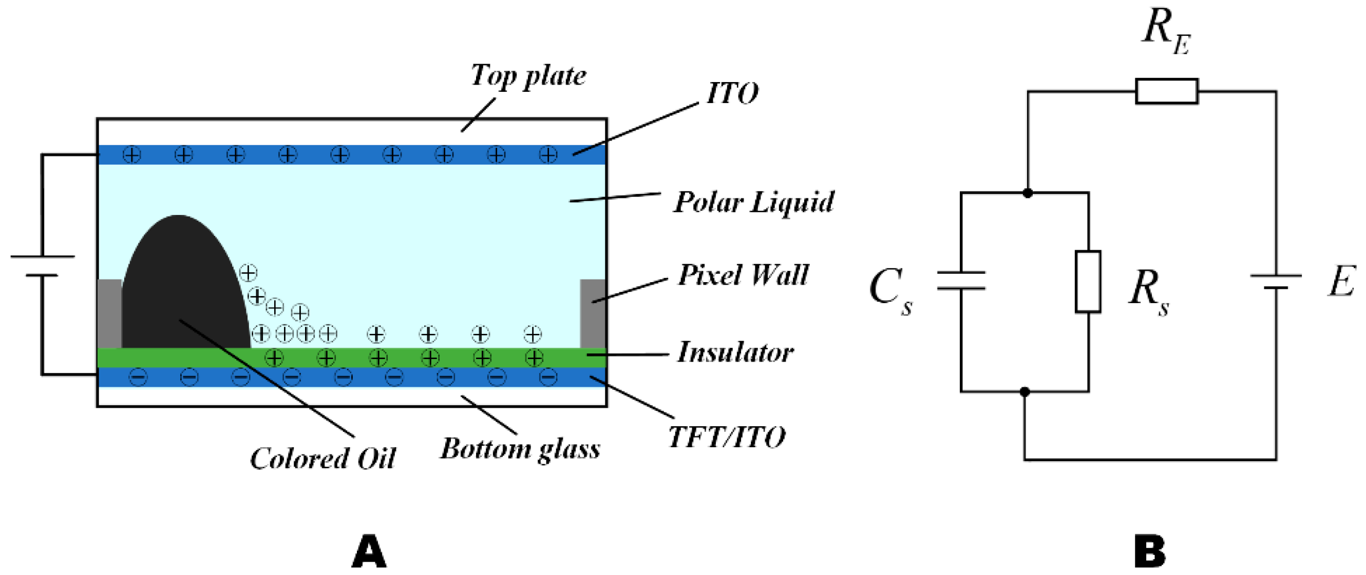
2. Principle of EWDs
2.1. Principle of EWDs
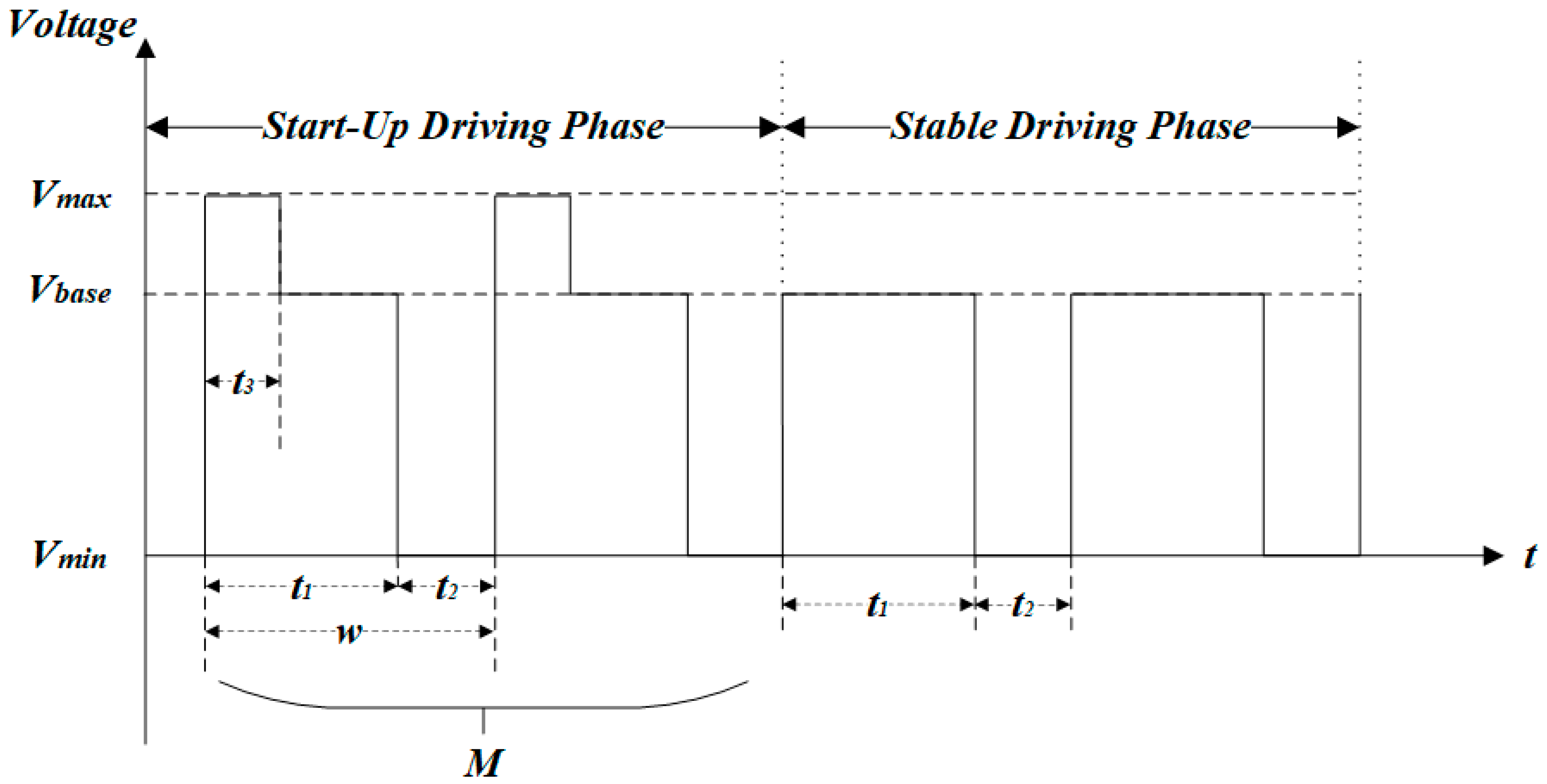
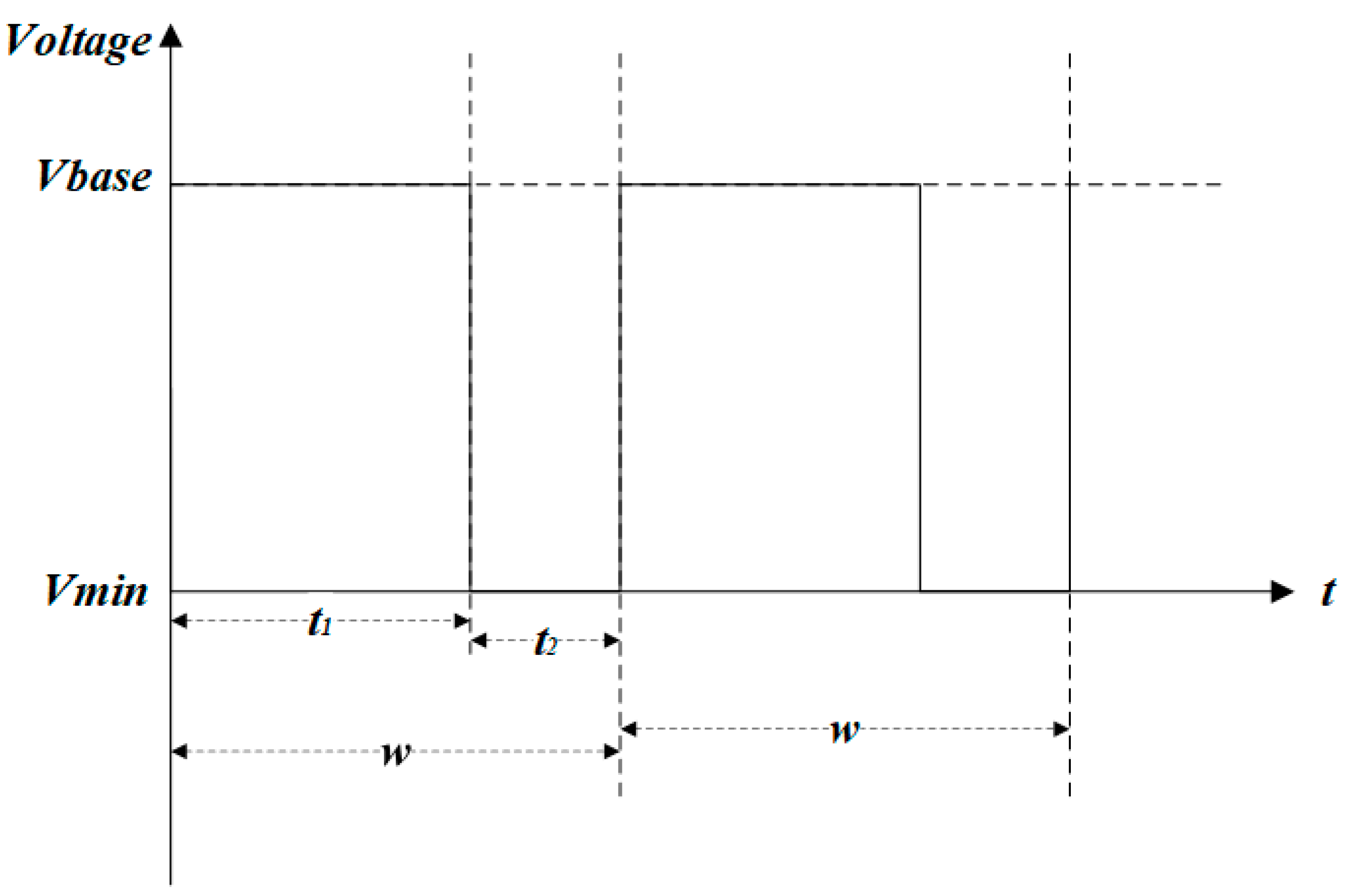
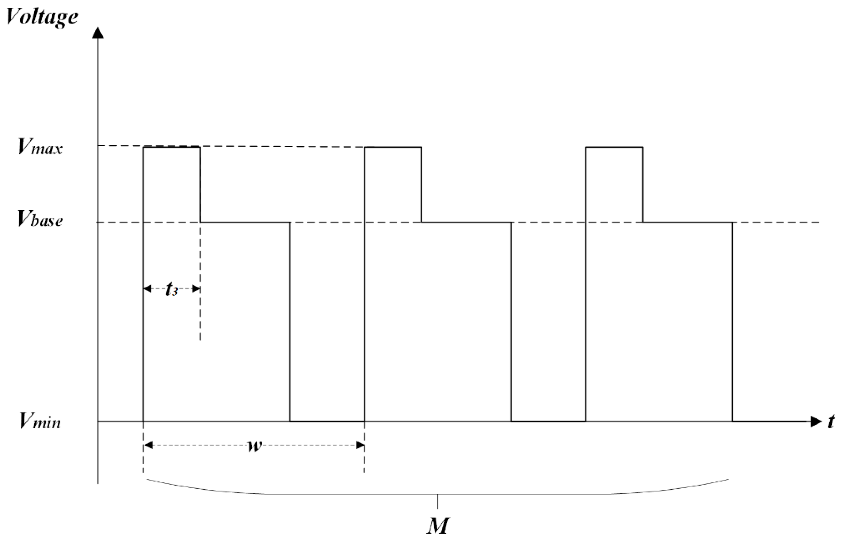
2.2. Multi-DC Driving Waveform
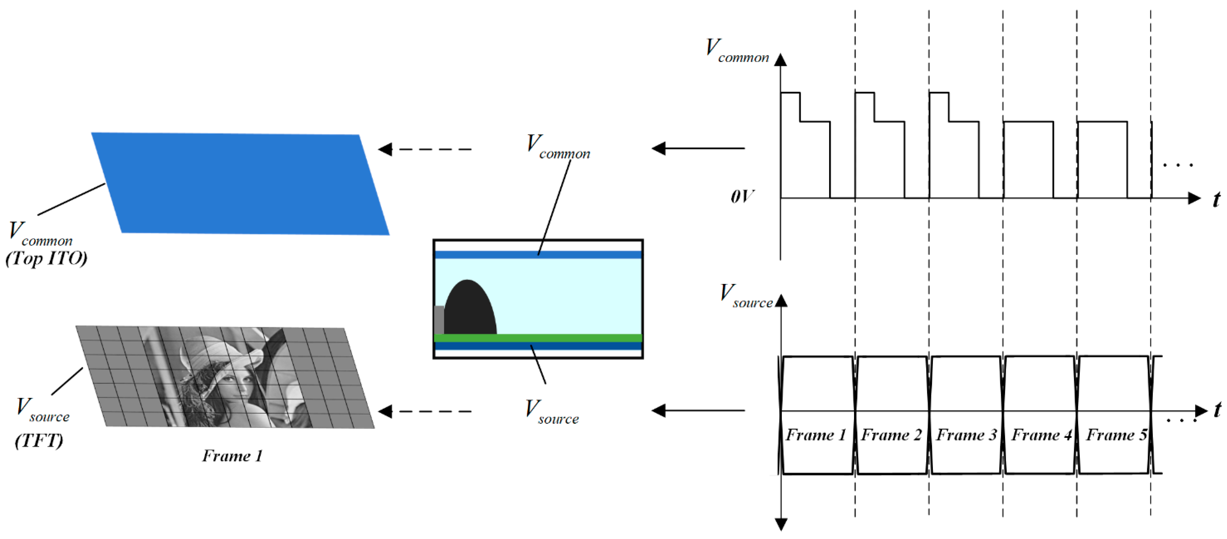
2.3. Multi-DC Driving Waveform Applied on the TFT-EWD
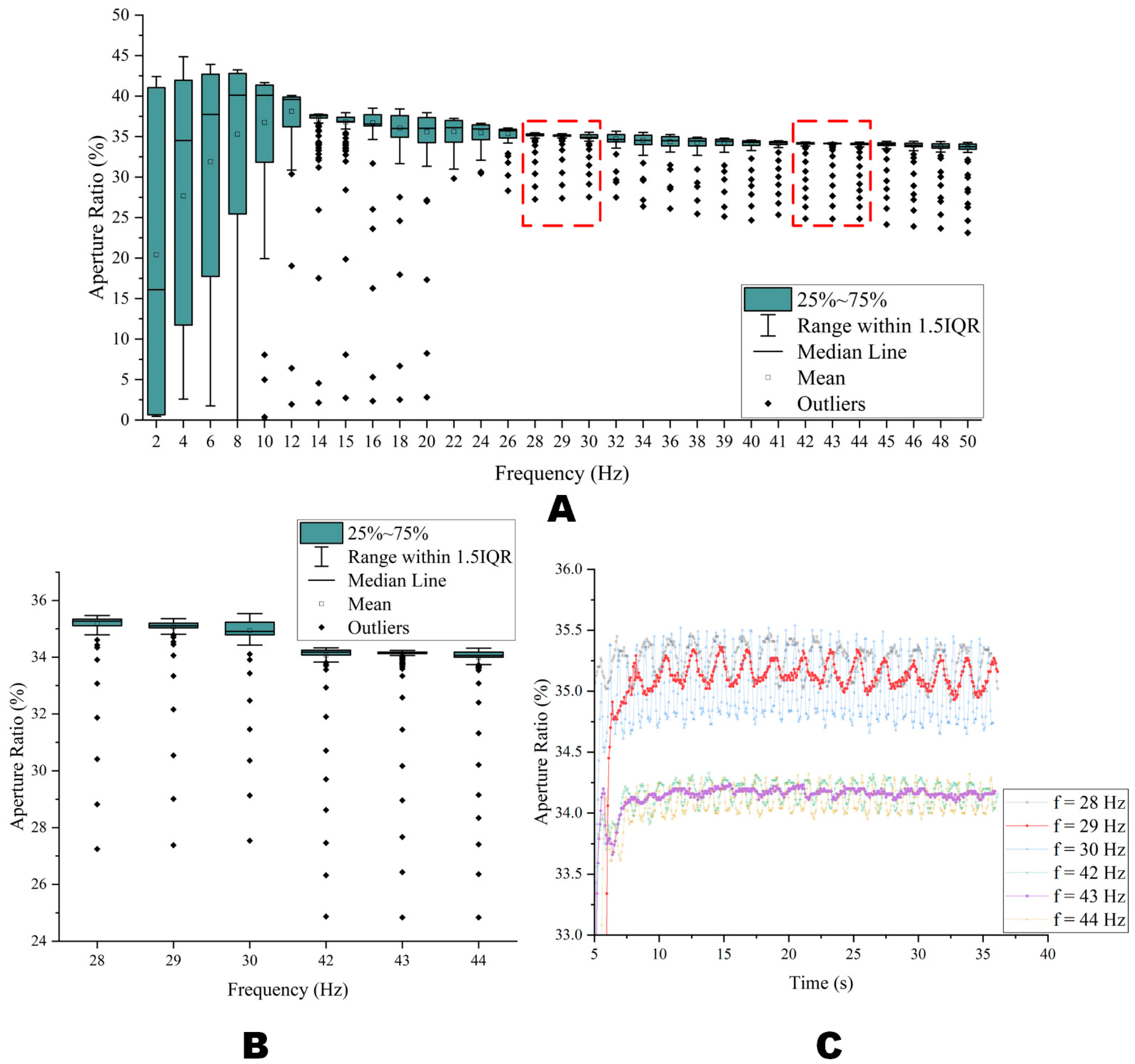
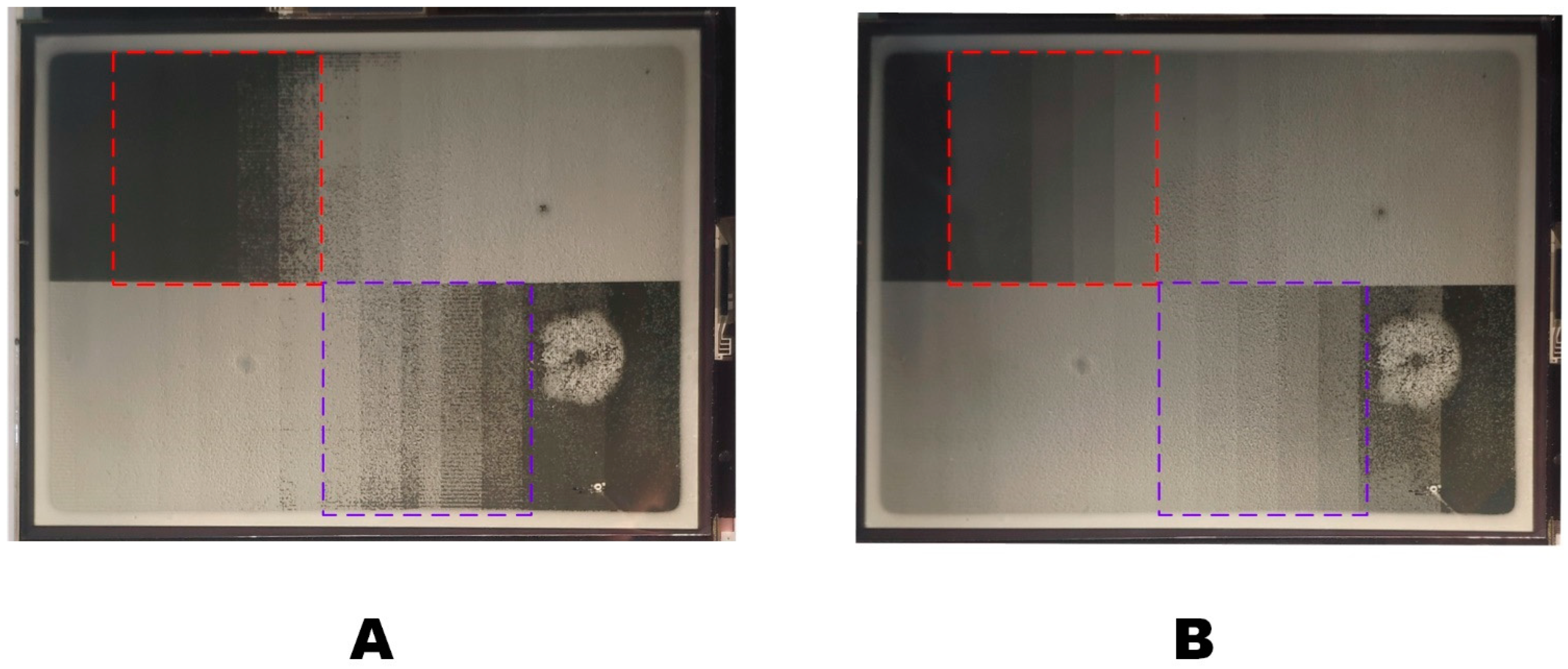
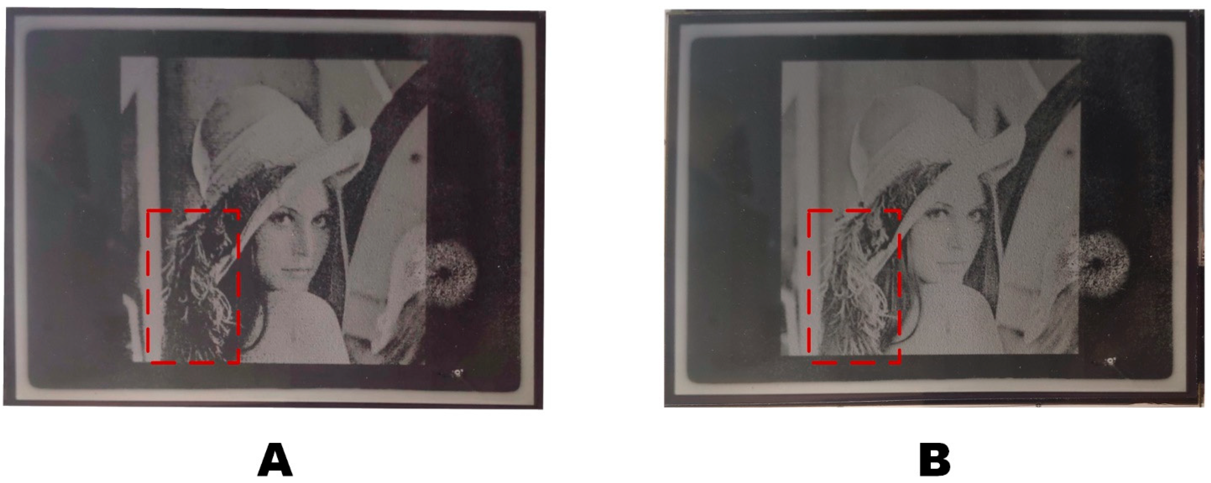
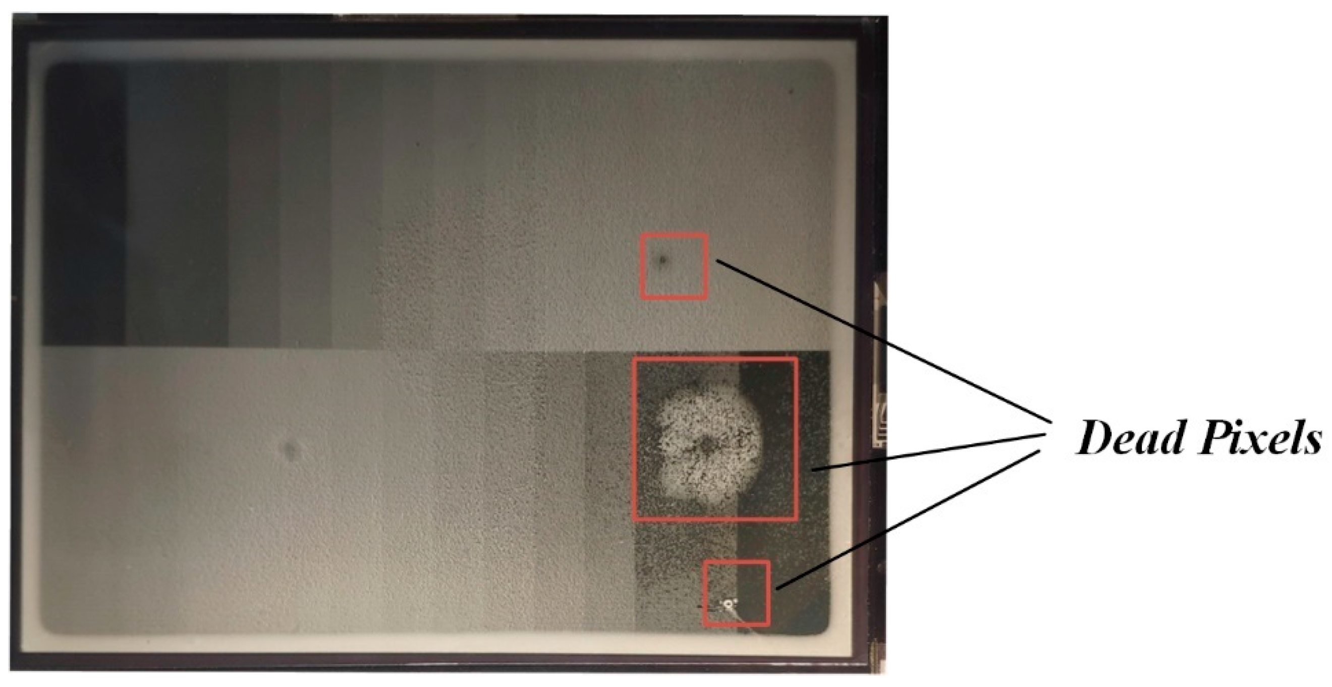
3. Results and Discussion
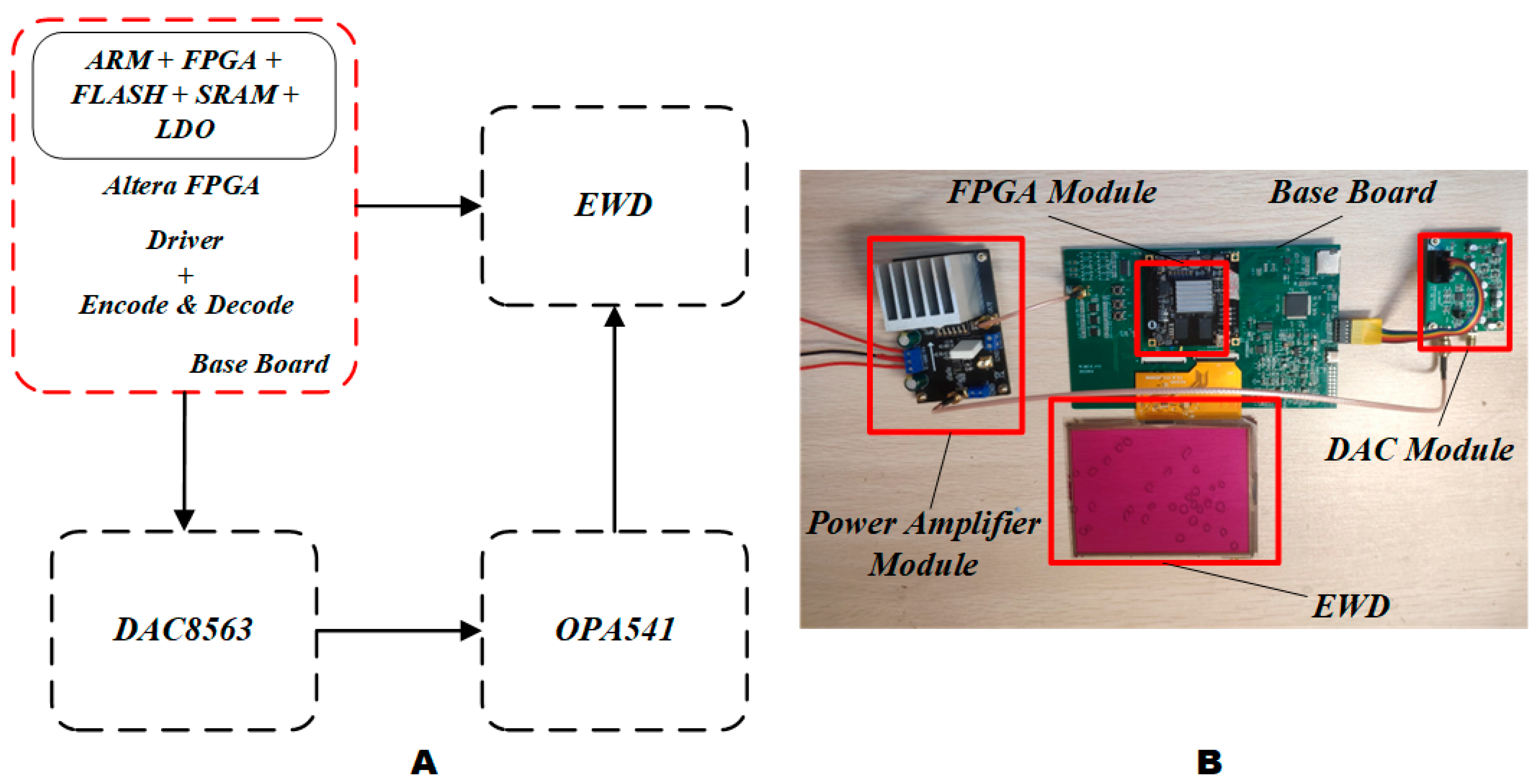
3.1. Experiment System
3.2. Stable Driving Phase Waveform
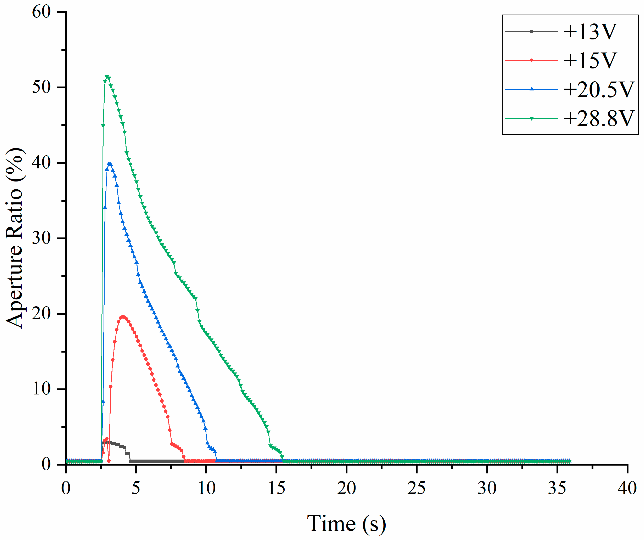
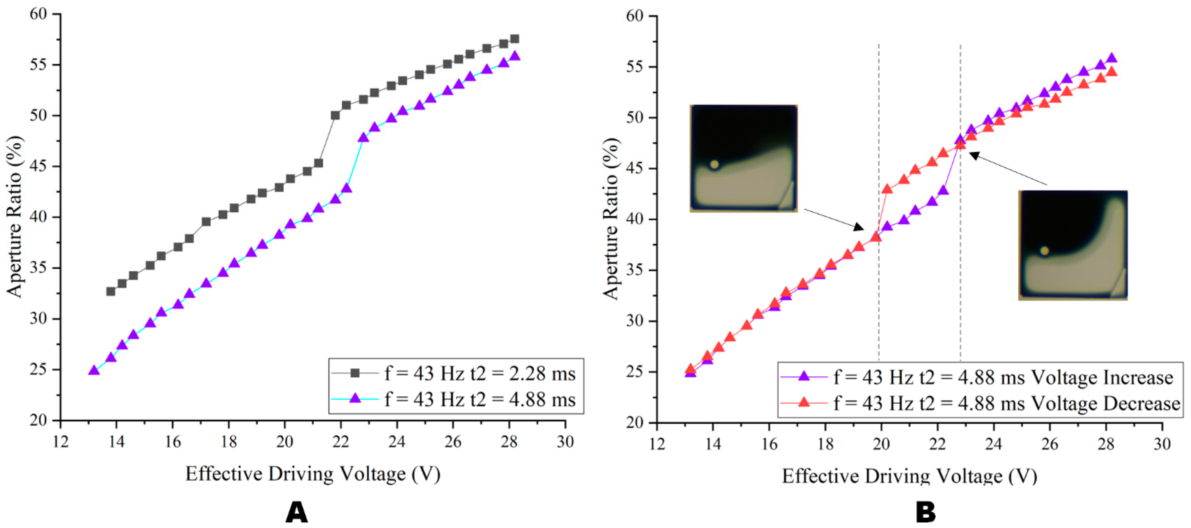
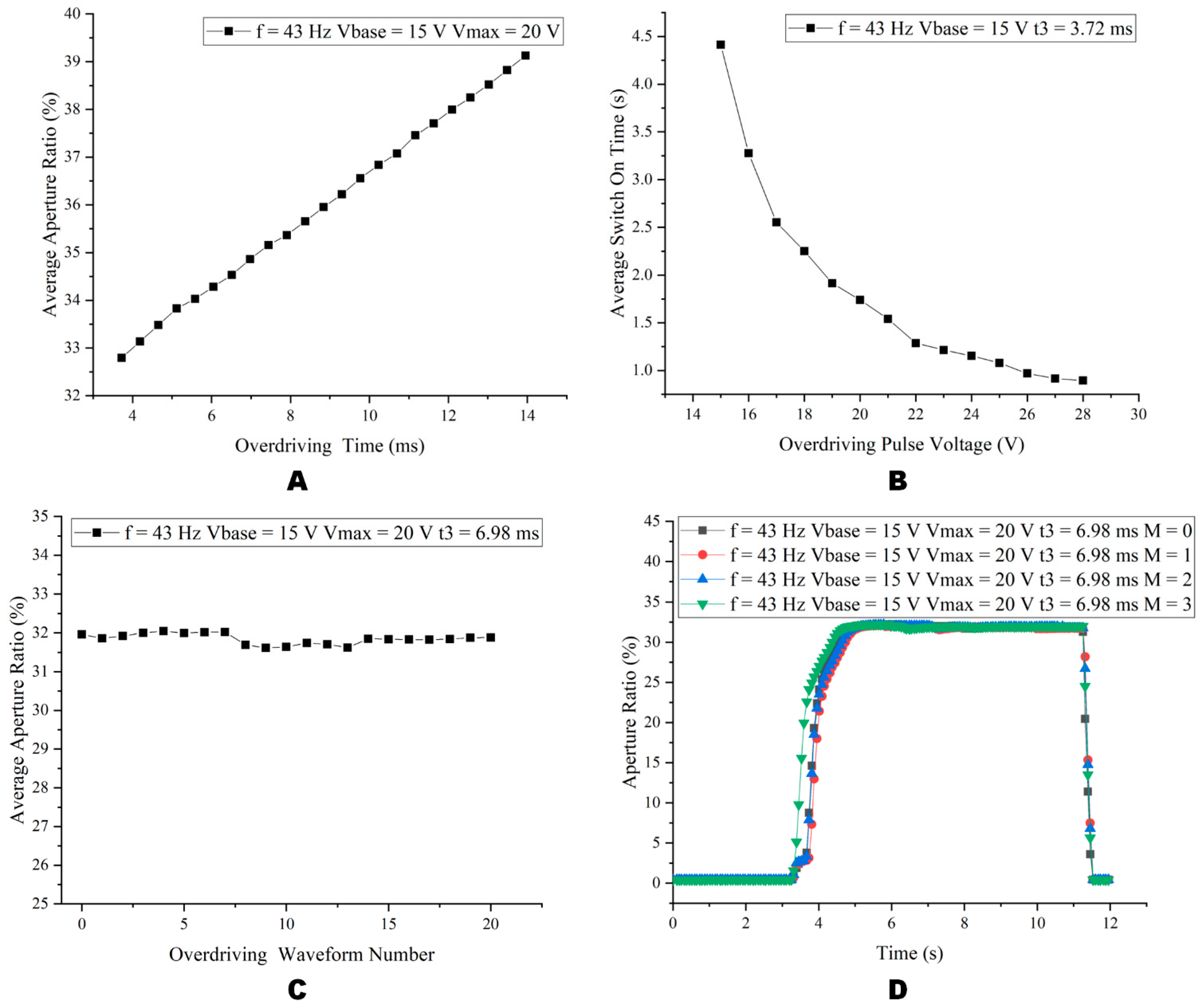
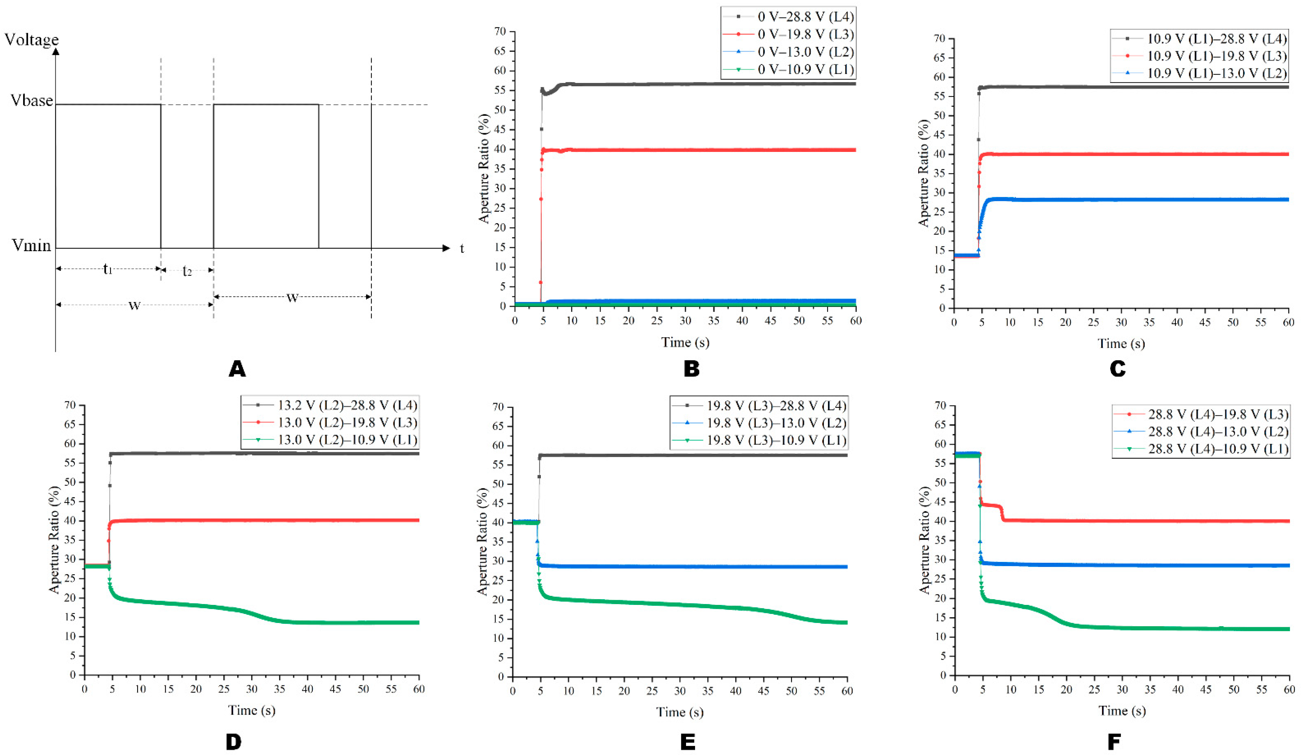
3.2.1. Driving Waveform Period ()
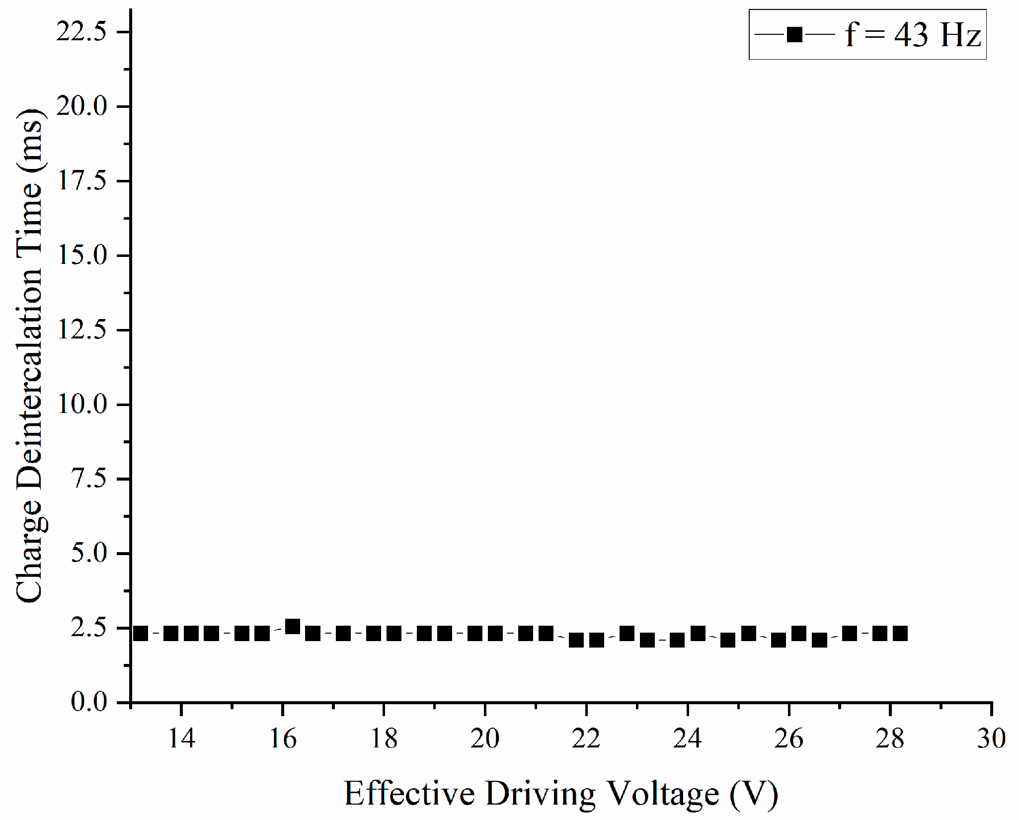
3.2.2. Charge Deintercalation Time ()
3.2.3. Effective Driving Voltage ()
3.3. Start-Up Driving Phase Waveform
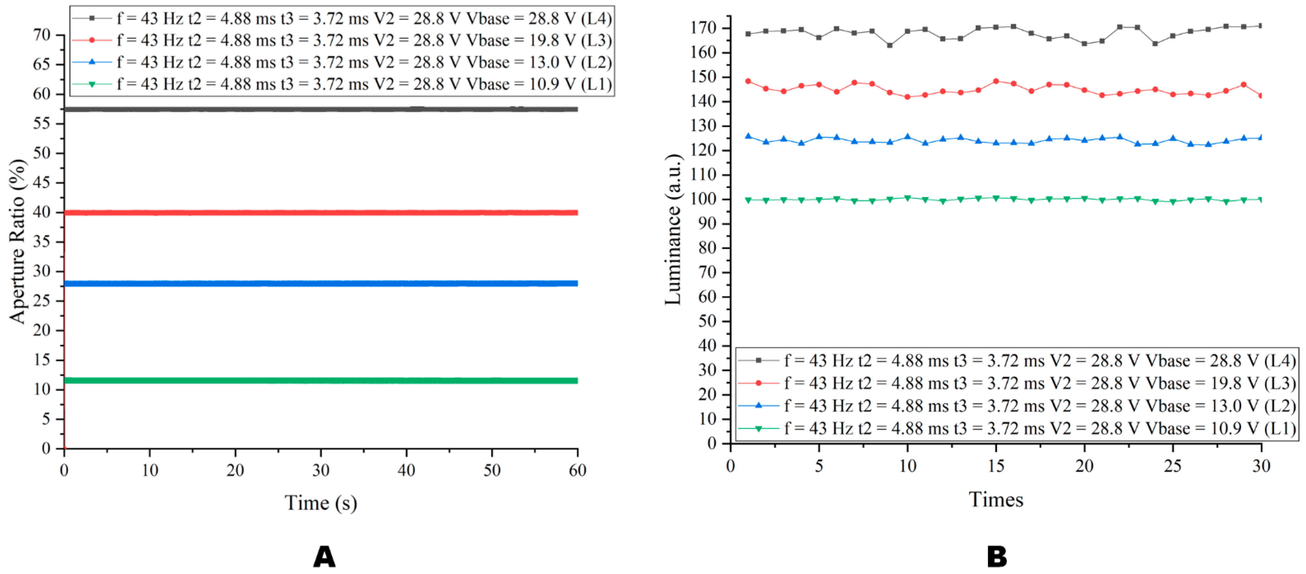
3.4. Multi-DC Driving Waveform Applied to TFT-EWD
4. Conclusions
Author Contributions
Funding
Data Availability Statement
Conflicts of Interest
References
- Guo, Y.; Tang, B.; Yuan, D.; Bai, P.; Li, H.; Yi, Z.; Deng, Y.; Zhou, R.; Zhong, B.; Jang, H.; et al. 3.1: Invited Paper: Electrowetting display: Towards full-color video reflective display. In Proceedings of the International Conference on Display Technology (ICDT 2021), Beijing, China, 30 May–2 June 2021; 52, pp. 59–63. [Google Scholar] [CrossRef]
- Bai, P.F.; Hayes, R.A.; Jin, M.L.; Shui, L.L.; Yi, Z.C.; Wang, L.; Zhang, X.; Zhou, G.F. Review of Paper-Like Display Technologies. Prog. Electromagn. Res.-Pier 2014, 147, 95–116. [Google Scholar] [CrossRef] [Green Version]
- Long, Z.; Yi, Z.; Zhang, H.; Lv, J.; Liu, L.; Chi, F.; Shui, L.; Zhang, C. Toward Suppressing Oil Backflow Based on a Combined Driving Waveform for Electrowetting Displays. Micromachines 2022, 13, 948. [Google Scholar] [CrossRef] [PubMed]
- Heikenfeld, J.; Drzaic, P.; Yeo, J.-S.; Koch, T. Review Paper: A critical review of the present and future prospects for electronic paper. J. Soc. Info. Disp. 2011, 19, 129–156. [Google Scholar] [CrossRef] [Green Version]
- Yi, Z.; Zhang, H.; Zeng, W.; Feng, H.; Long, Z.; Liu, L.; Hu, Y.; Zhou, X.; Zhang, C. Review of Driving Waveform for Electrowetting Displays. Front. Phys. 2021, 9, 728804. [Google Scholar] [CrossRef]
- Yi, Z.; Zeng, W.; Ma, S.; Feng, H.; Zeng, W.; Shen, S.; Shui, L.; Zhou, G.; Zhang, C. Design of Driving Waveform Based on a Damping Oscillation for Optimizing Red Saturation in Three-Color Electrophoretic Displays. Micromachines 2021, 12, 162. [Google Scholar] [CrossRef] [PubMed]
- Zhang, T.; Guo, Y.; Deng, Y.; Sun, H. An extensible driving model for multiple grayscales colorful electrowetting displays. Front. Phys. 2022, 10, 1077. [Google Scholar] [CrossRef]
- Beni, G.; Hackwood, S. Electro-wetting displays. Appl. Phys. Lett. 1981, 38, 207–209. [Google Scholar] [CrossRef]
- Hayes, R.A.; Feenstra, B.J. Video-speed electronic paper based on electrowetting. Nature 2003, 425, 383–385. [Google Scholar] [CrossRef]
- Feng, H.; Yi, Z.; Yang, R.; Qin, X.; Shen, S.; Zeng, W.; Shui, L.; Zhou, G.; Zhang, C. Designing Splicing Digital Microfluidics Chips Based on Polytetrafluoroethylene Membrane. Micromachines 2020, 11, 1067. [Google Scholar] [CrossRef]
- Torabinia, M.; Asgari, P.; Dakarapu, U.S.; Jeon, J.; Moon, H. On-chip organic synthesis enabled using an engine-and-cargo system in an electrowetting-on-dielectric digital microfluidic device. Lab Chip 2019, 19, 3054–3064. [Google Scholar] [CrossRef]
- Berge, B. Liquid lens technology: Principle of electrowetting based lenses and applications to imaging. In Proceedings of the 18th IEEE International Conference on Micro Electro Mechanical Systems, MEMS 2005, Miami Beach, FL, USA, 30 January–3 February 2005; pp. 227–230. [Google Scholar]
- Hu, X.; Zhang, S.; Qu, C.; Zhang, Q.; Lu, L.; Ma, X.; Zhang, X.; Deng, Y. Ionic liquid based variable focus lenses. Soft Matter 2011, 7, 5941–5943. [Google Scholar] [CrossRef]
- Qian, M.; Lin, S.; Zeng, S.; Lin, Z.; Guo, T.; Tang, B. Real-time dynamic driving system implementation of electrowetting display. Opto-Electron. Eng. 2019, 46, 180623. [Google Scholar] [CrossRef]
- Zhou, R.; Fu, S.; Jiang, H.; Li, X.; Zhou, G. Thermal accelerated aging study of water/fluoropolymer/ITO contact in electrowetting display systems. Results Phys. 2019, 15, 102737. [Google Scholar] [CrossRef]
- Tian, L.; Zhang, H.; Yi, Z.; Zhang, B.; Zhou, R.; Zhou, G.; Gong, J. Inhibiting Oil Splitting and Backflow in Electrowetting Displays by Designing a Power Function Driving Waveform. Electronics 2022, 11, 2081. [Google Scholar] [CrossRef]
- Wang, L.; Zhang, H.; Li, W.; Li, J.; Yi, Z.; Wan, Q.; Zhang, J.; Ma, P. Driving Scheme Optimization for Electrowetting Displays Based on Contact Angle Hysteresis to Achieve Precise Gray-Scales. Front. Phys. 2021, 9, 655547. [Google Scholar] [CrossRef]
- Li, S.; Xu, Y.; Zhan, Z.; Liu, L.; Bai, P. A high integration electrowetting displays system based on AC driving model. Front. Phys. 2022, 10, 1009. [Google Scholar] [CrossRef]
- Liu, L.; Wu, Z.; Wang, L.; Zhang, T.; Li, W.; Lai, S.; Bai, P. Design of an AC Driving Waveform Based on Characteristics of Electrowetting Stability for Electrowetting Displays. Front. Phys. 2020, 8, 618752. [Google Scholar] [CrossRef]
- Yi, Z.; Shui, L.; Wang, L.; Jin, M.; Hayes, R.A.; Zhou, G. A novel driver for active matrix electrowetting displays. Displays 2015, 37, 86–93. [Google Scholar] [CrossRef]
- Zhang, T.; Deng, Y. Driving Waveform Design of Electrowetting Displays Based on a Reset Signal for Suppressing Charge Trapping Effect. Front. Phys. 2021, 9, 672541. [Google Scholar] [CrossRef]
- Li, W.; Wang, L.; Henzen, A. A Multi Waveform Adaptive Driving Scheme for Reducing Hysteresis Effect of Electrowetting Displays. Front. Phys. 2020, 8, 618811. [Google Scholar] [CrossRef]
- Chiu, Y.-H.; Liang, C.-C.; Chen, Y.-C.; Lee, W.-Y.; Chen, H.-Y.; Wu, S.-H. Accurate-gray-level and quick-response driving methods for high-performance electrowetting displays. J. Soc. Inf. Disp. 2011, 19, 741–748. [Google Scholar] [CrossRef]
- Li, S.; Xu, Y.; Zhan, Z.; Du, P.; Liu, L.; Li, Z.; Wang, H.; Bai, P. Dynamic Adaptive Display System for Electrowetting Displays Based on Alternating Current and Direct Current. Micromachines 2022, 13, 1791. [Google Scholar] [CrossRef] [PubMed]
- Verheijen, H.J.J.; Prins, M.W.J. Reversible Electrowetting and Trapping of Charge: Model and Experiments. Langmuir 1999, 15, 6616–6620. [Google Scholar] [CrossRef] [Green Version]
- Zhao, Q.; Tang, B.; Dong, B.Q.; Li, H.; Zhou, R.; Guo, Y.Y.; Dou, Y.Y.; Deng, Y.; Groenewold, J.; Henzen, A.V.; et al. Electrowetting on dielectric: Experimental and model study of oil conductivity on rupture voltage. J. Phys. D-Appl. Phys. 2018, 51, 195102. [Google Scholar] [CrossRef]
- Zeng, W.; Yi, Z.; Zhao, Y.; Zeng, W.; Ma, S.; Zhou, X.; Feng, H.; Liu, L.; Shui, L.; Zhang, C.; et al. Design of Driving Waveform Based on Overdriving Voltage for Shortening Response Time in Electrowetting Displays. Front. Phys. 2021, 9, 642682. [Google Scholar] [CrossRef]
- Li, W.; Wang, L.; Zhang, T.; Lai, S.; Liu, L.; He, W.; Zhou, G.; Yi, Z. Driving Waveform Design with Rising Gradient and Sawtooth Wave of Electrowetting Displays for Ultra-Low Power Consumption. Micromachines 2020, 11, 145. [Google Scholar] [CrossRef] [Green Version]
- Chen, C.-H.; Tsai, S.-L.; Chen, M.-K.; Jang, L.-S.J.S.; Chemical, A.B. Effects of gap height, applied frequency, and fluid conductivity on minimum actuation voltage of electrowetting-on-dielectric and liquid dielectrophoresis. Sens. Actuators B: Chem. 2011, 159, 321–327. [Google Scholar] [CrossRef]
- Kumar, A.; Pluntke, M.; Cross, B.; Baret, J.-C.; Mugele, F.J.M.O.P.L. Finite conductivity effects and apparent contact angle saturation in AC electrowetting. MRS Online Proc. Libr. 2005, 899, 601. [Google Scholar] [CrossRef]
- Liang, C.C.; Chen, Y.C.; Chiu, Y.H.; Chen, H.Y.; Cheng, W.Y.; Lee, W.Y. 27.3: A Decoupling Driving Scheme for Low Voltage Stress in Driving a Large-Area High-Resolution Electrowetting Display. In SID Symposium Digest of Technical Papers; Blackwell Publishing Ltd.: Oxford, UK, 2009; pp. 375–378. [Google Scholar]
- Li, X.; Tian, H.; Shao, J.; Ding, Y.; Chen, X.; Wang, L.; Lu, B. Decreasing the Saturated Contact Angle in Electrowetting-on-Dielectrics by Controlling the Charge Trapping at Liquid-Solid Interfaces. Adv. Funct. Mater. 2016, 26, 2994–3002. [Google Scholar] [CrossRef]
- Chen, Y.C.; Chiu, Y.H.; Lee, W.Y.; Liang, C.C. 56.3: A charge trapping suppression method for quick response electrowetting displays. In SID Symposium Digest of Technical Papers; Blackwell Publishing Ltd.: Oxford, UK, 2010; pp. 842–845. [Google Scholar]
- Feenstra, J. Video-Speed Electrowetting Display Technology. In Handbook of Visual Display Technology; Chen, J., Cranton, W., Fihn, M., Eds.; Springer: Berlin/Heidelberg, Germany, 2012; pp. 1731–1745. [Google Scholar]
- Jiang, J.-W.; Xie, C.-M.; Xu, L.-H.; Li, L.; Huang, W.-X. The groove at blade tip designed for suppression of tip-leakage vortex may bring the risk of inducing new cavitation. Phys. Fluids 2022, 34, 121701. [Google Scholar] [CrossRef]
- Wang, Q.; Li, L.; Gu, J.; Zhang, C.; Lyu, J.; Yao, W. Manipulation of a Nonconductive Droplet in an Aqueous Fluid with AC Electric Fields: Droplet Dewetting, Oscillation, and Detachment. Langmuir 2021, 37, 12098–12111. [Google Scholar] [CrossRef] [PubMed]
- Kashina, M.A.; Alabuzhev, A.A. The Forced Oscillations of an Oblate Drop Sandwiched Between Different Inhomogeneous Surfaces under AC Vibrational Force. Microgravity Sci. Technol. 2021, 33, 35. [Google Scholar] [CrossRef]
- Roques-Carmes, T.; Hayes, R.A.; Feenstra, B.J.; Schlangen, L.J.M. Liquid behavior inside a reflective display pixel based on electrowetting. J. Appl. Phys. 2004, 95, 4389–4396. [Google Scholar] [CrossRef]
- Long, Z.; Yi, Z.; Zhang, H.; Liu, L.; Shui, L. Toward Suppressing Charge Trapping Based on a Combined Driving Waveform with an AC Reset Signal for Electro-Fluidic Displays. Membranes 2022, 12, 1072. [Google Scholar] [CrossRef]
- Guo, Y.; Jiang, H.; Yuan, D.; Tang, B.; Zhou, G. Progress in electrowetting display materials and device technology. Chin. J. Liq. Cryst. Disp. 2022, 37, 925–941. [Google Scholar] [CrossRef]


| Sample Number | Process Conditions | Characteristic of Oil | Pixel Wall Height (µm) | Oil Droplet | Aperture Ratio (DC 30 V) | ||
|---|---|---|---|---|---|---|---|
| Descum Parameter | Reflow Temperature | Oil Color | Concentration | ||||
| ITO-EWD | 100 W/100 S | 185 °C/2H | Black | 18% | 3.5 | 18 | 61.48% |
| TFT-EWD | 100 W/100 S | 210 °C/1H | Black | 18% | 3.5 | 18 | \ |
Disclaimer/Publisher’s Note: The statements, opinions and data contained in all publications are solely those of the individual author(s) and contributor(s) and not of MDPI and/or the editor(s). MDPI and/or the editor(s) disclaim responsibility for any injury to people or property resulting from any ideas, methods, instructions or products referred to in the content. |
© 2023 by the authors. Licensee MDPI, Basel, Switzerland. This article is an open access article distributed under the terms and conditions of the Creative Commons Attribution (CC BY) license (https://creativecommons.org/licenses/by/4.0/).
Share and Cite
Xu, Y.; Li, S.; Wang, Z.; Zhang, H.; Li, Z.; Xiao, B.; Guo, W.; Liu, L.; Bai, P. Design of Multi-DC Overdriving Waveform of Electrowetting Displays for Gray Scale Consistency. Micromachines 2023, 14, 684. https://doi.org/10.3390/mi14030684
Xu Y, Li S, Wang Z, Zhang H, Li Z, Xiao B, Guo W, Liu L, Bai P. Design of Multi-DC Overdriving Waveform of Electrowetting Displays for Gray Scale Consistency. Micromachines. 2023; 14(3):684. https://doi.org/10.3390/mi14030684
Chicago/Turabian StyleXu, Yijian, Shixiao Li, Ziyang Wang, Heng Zhang, Zikai Li, Bo Xiao, Wei Guo, Linwei Liu, and Pengfei Bai. 2023. "Design of Multi-DC Overdriving Waveform of Electrowetting Displays for Gray Scale Consistency" Micromachines 14, no. 3: 684. https://doi.org/10.3390/mi14030684