
Bi2Te3 Thin Films Deposited by the Combination of Bi and Te Plasmas in a PLD Process

 , , ,
, , , 
Abstract
:1. Introduction
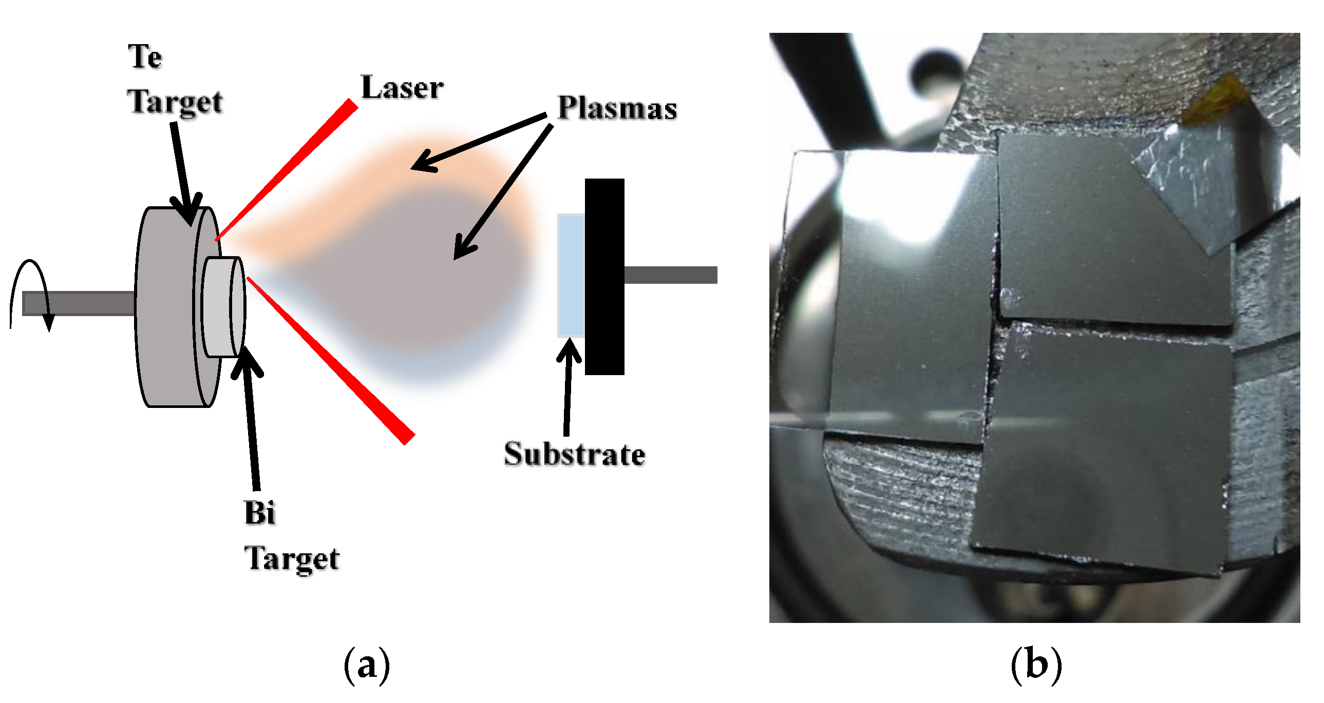
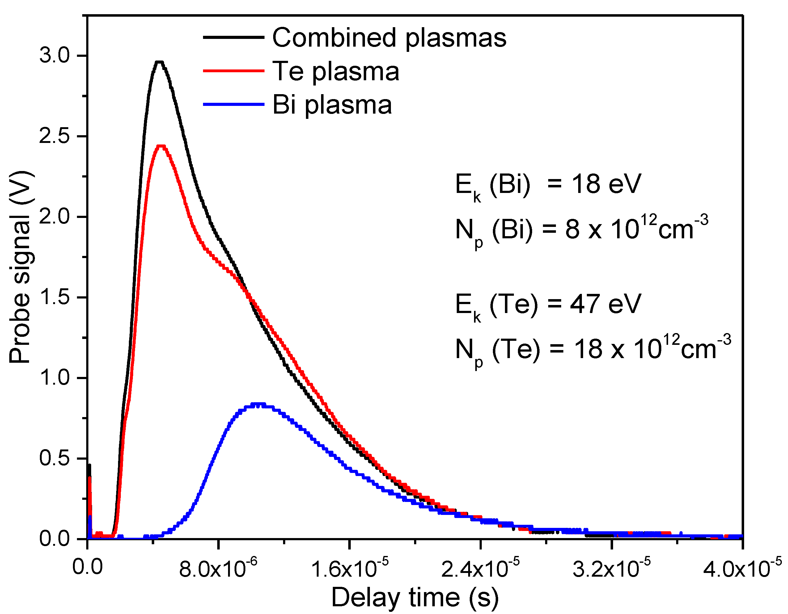
2. Materials and Methods
3. Results and Discussion
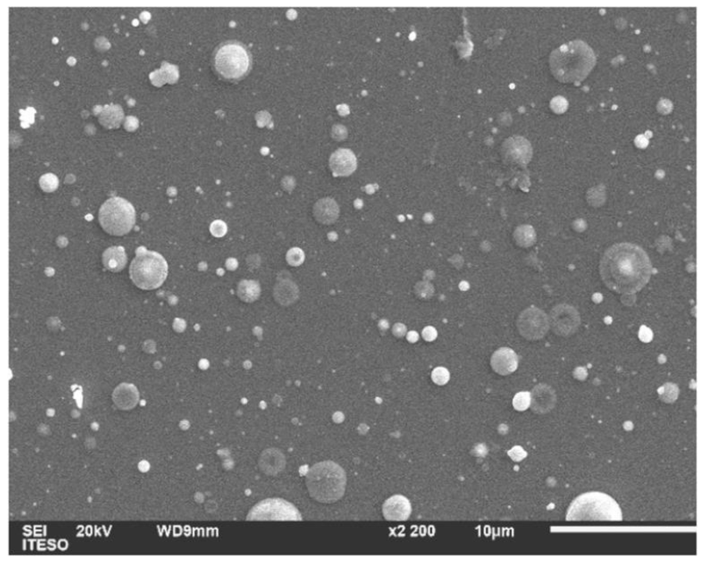
3.1. Scanning Electron Microscopy
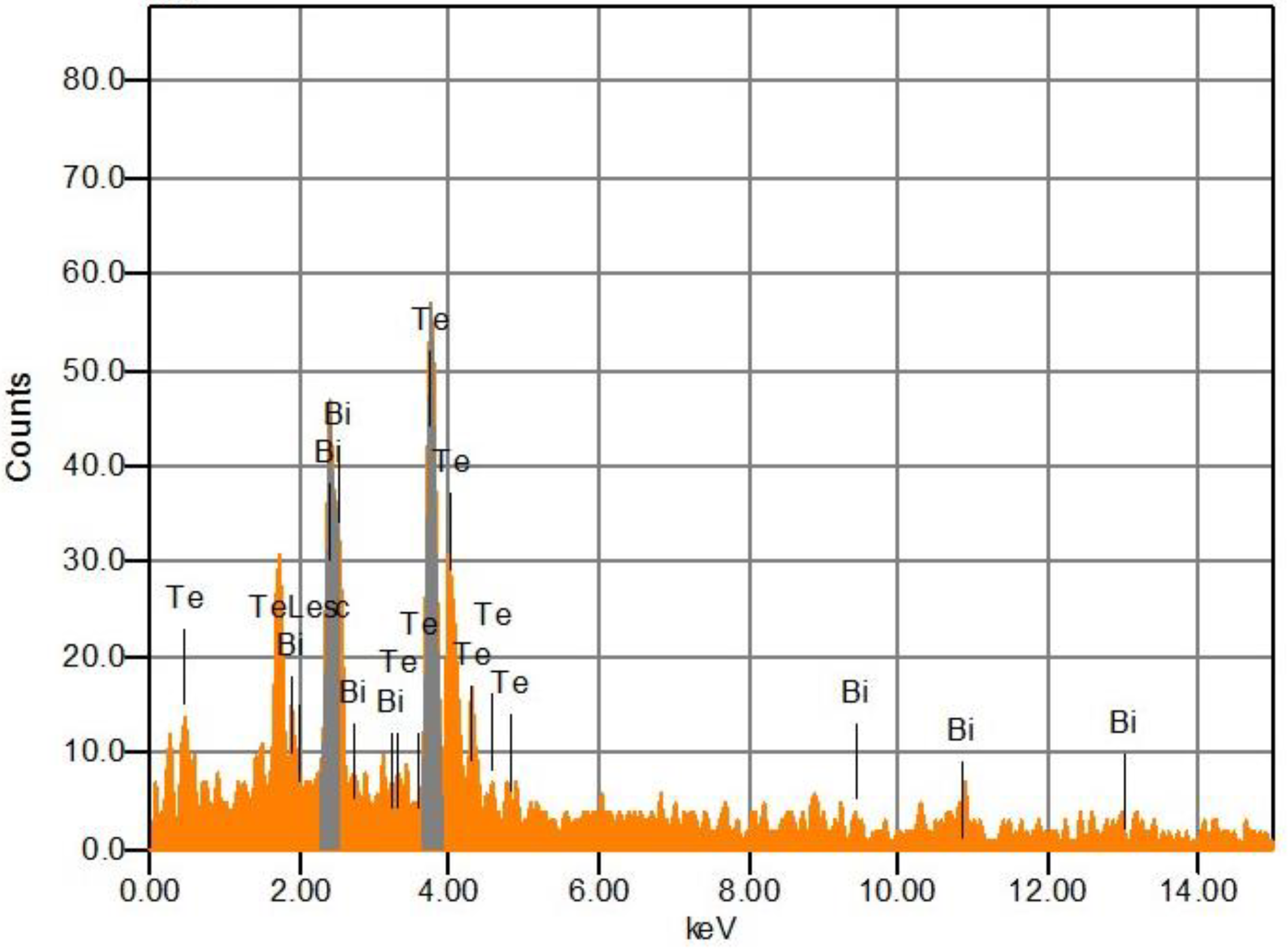
3.2. EDS Analysis
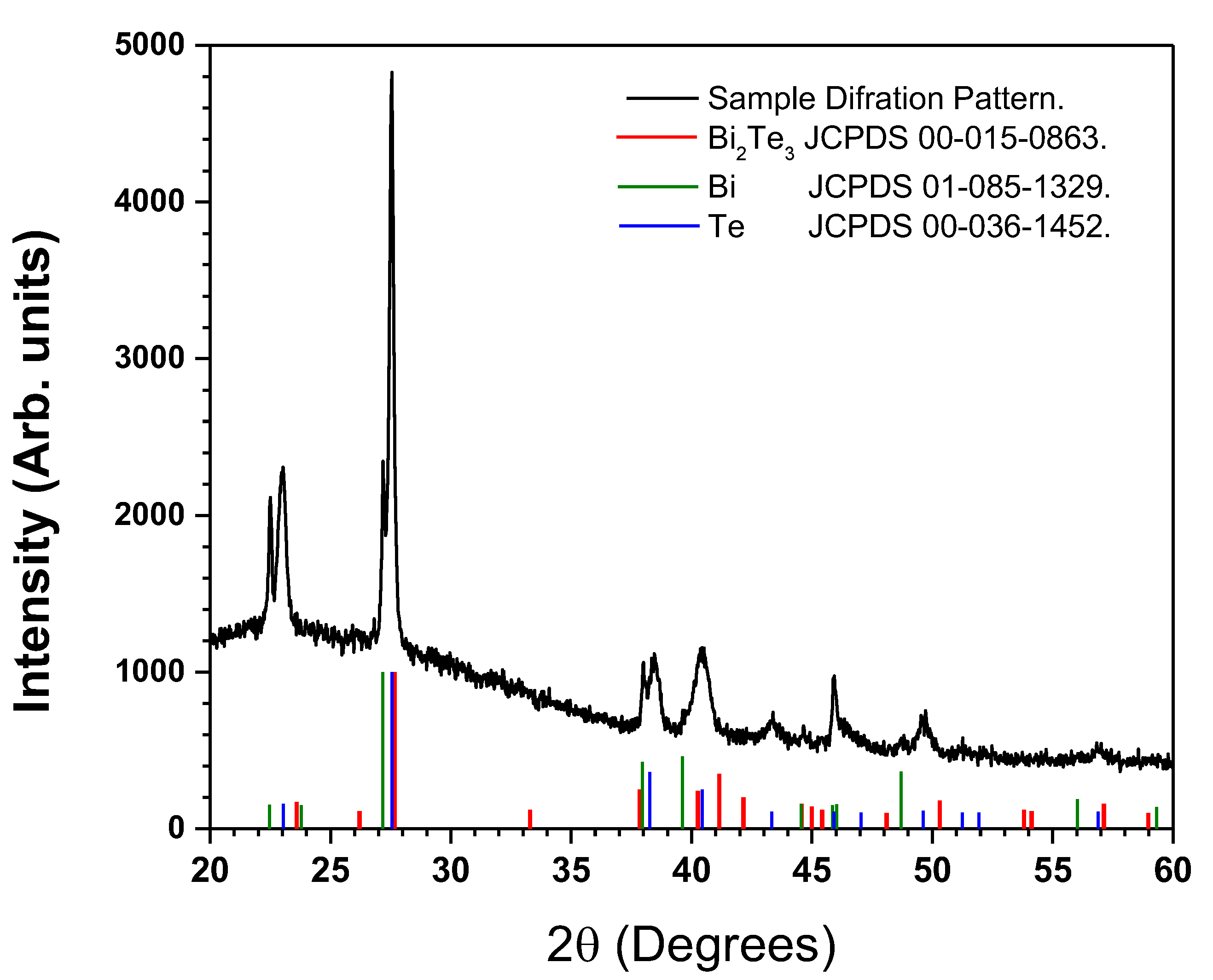
3.3. XRD Analysis
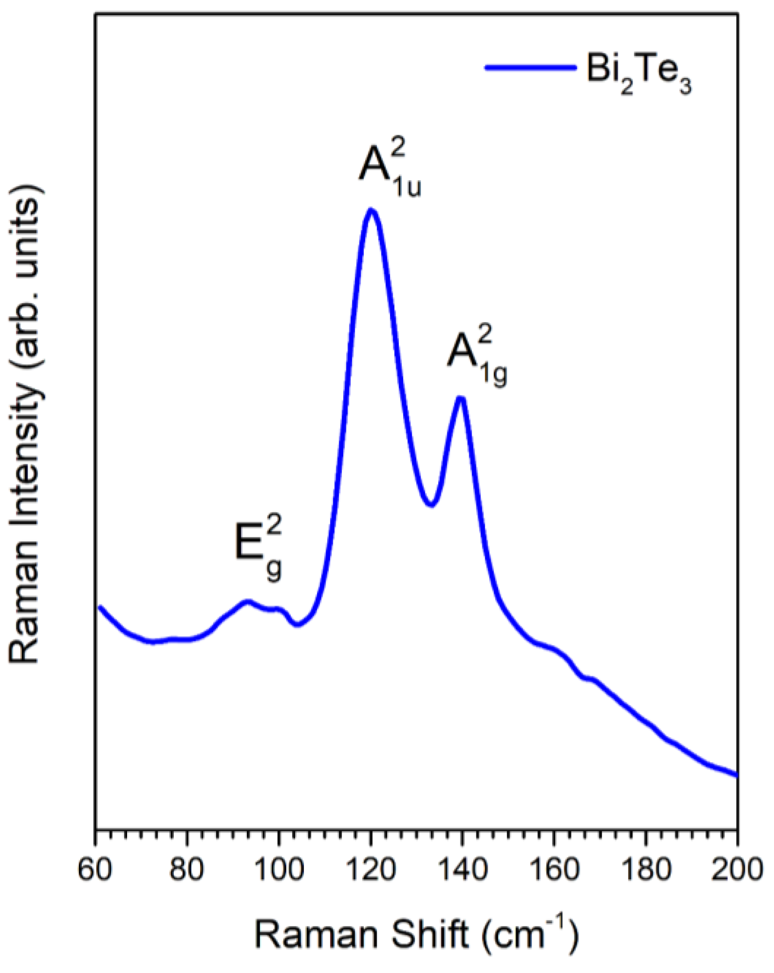
3.4. Raman Analysis
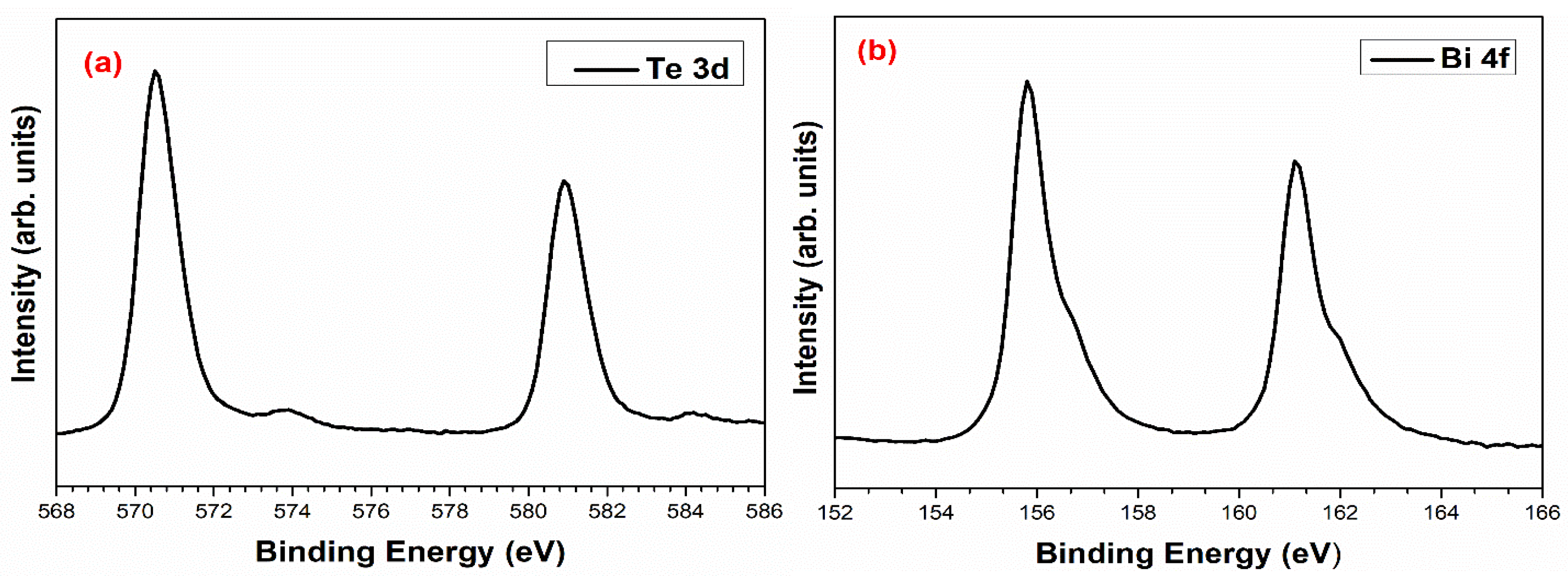
3.5. XPS Analysis
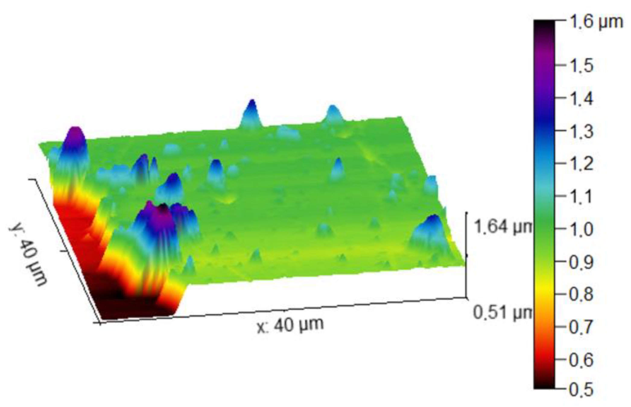
3.6. AFM Analysis
4. Conclusions
Author Contributions
Funding
Data Availability Statement
Acknowledgments
Conflicts of Interest
References
- Liang, Y.; Wang, W.; Zeng, B.; Zhang, G.; Huang, J.; Li, J.; Li, T.; Song, Y.; Zhang, X. Raman scattering investigation of Bi2Te3 hexagonal nanoplates prepared by a solvothermal process in the absence of NaOH. J. Alloys Compd. 2011, 509, 5147–5151. [Google Scholar] [CrossRef]
- Kullmann, W.; Geurts, J.; Richter, W.; Lehner, N.; Rauh, H.; Steigenberger, U.; Eichhorn, G.; Geick, R. Effect of Hydrostatic and Uniaxial Pressure on Structural Properties and Raman Active Lattice Vibrations in Bi2Te3. Phys. Stat. Sol. B 1984, 125, 131. [Google Scholar] [CrossRef]
- Witting, I.T.; Chasapis, T.C.; Ricci, F.; Peters, M.; Heinz, N.A.; Hautier, G.; Snyder, G.J. The Thermoelectric Properties of Bismuth Telluride. Adv. Electron. Mater. 2019, 5, 1800904. [Google Scholar] [CrossRef]
- Lee, S.; Esfarjani, K.; Luo, T.; Zhou, J.; Tian, Z.; Chen, G. Resonant bonding leads to low lattice thermal conductivity. Nat. Commun. 2014, 5, 3525. [Google Scholar] [CrossRef] [Green Version]
- Zeier, W.G.; Zevalkink, A.; Gibbs, Z.M.; Hautier, G.; Kanatzidis, M.G.; Snyder, G.J. Thinking Like a Chemist: Intuition in Thermoelectric Materials. Angew. Chem. Int. Ed. 2016, 55, 6826. [Google Scholar] [CrossRef]
- Scidone, L.; Diliberto, S.; Stein, N.; Boulanger, C.; Lecuire, J.M. Electroless method for Bi2Te3 film deposition. Mat. Lett. 2005, 59, 746–748. [Google Scholar] [CrossRef]
- Kang, W.-S.; Chou, W.-C.; Li, W.-J.; Shen, T.-H.; Lin, C.-S. Electrodeposition of Bi2Te3-based p and n-type ternary thermoelectric compounds in chloride baths. Thin Solid Films 2018, 660, 108–119. [Google Scholar] [CrossRef]
- Zhao, Y.-J.; Zhou, F. Synthesis, Evolution of Morphology, Transport Properties for Bi2Te3 Nanoplates. Crystals 2022, 12, 1668. [Google Scholar] [CrossRef]
- Yan, Z.; Chrisey, D.B. Pulsed laser ablation in liquid for micro-/nanostructure generation. J. Photochem. Photobiol. C Photochem. Rev. 2012, 13, 204–223. [Google Scholar] [CrossRef]
- Lowndes, D.H.; Geohegan, D.B.; Puretzky, A.A.; Norton, D.P.; Rouleau, C.M. Synthesis of Novel Thin-Film Materials by Pulsed Laser Deposition. Science 1996, 273, 898. [Google Scholar] [CrossRef] [Green Version]
- Wicklein, S.; Sambri, A.; Amoruso, S.; Wang, X.; Bruzzese, R.; Koehl, A.; Dittmann, R. Pulsed laser ablation of complex oxides: The role of congruent ablation and preferential scattering for the film stoichiometry. Appl. Phys. Lett. 2012, 101, 131601. [Google Scholar] [CrossRef] [Green Version]
- Quiñones-Galván, J.G.; Lozada-Morales, R.; Jiménez-Sandoval, S.; Camps, E.; Castrejón-Sánchez, V.H.; Campos-González, E.; Zapata-Torres, M.; Pérez-Centeno, A.; Santana-Aranda, M.A. Physical properties of a non-transparent cadmium oxide thick film deposited at low fluence by pulsed laser deposition. Mat. Res. Bull. 2016, 76, 376–383. [Google Scholar] [CrossRef]
- Quiñones-Galván, J.G.; Camps, E.; Campos-González, E.; Hernández-Hernández, A.; Santana-Aranda, M.A.; Pérez-Centeno, A.; Guillén-Cervantes, A.; Santoyo-Salazar, J.; Zelaya-Angel, O.; de Moure-Flores, F. Influence of plasma parameters and substrate temperature on the structural and optical properties of CdTe thin films deposited on glass by laser ablation. J. Appl. Phys. 2015, 118, 125304. [Google Scholar] [CrossRef]
- Le, P.H.; Liao, C.-N.; Luo, C.W.; Leu, J. Thermoelectric properties of nanostructured bismuth–telluride thin films grown using pulsed laser deposition. J. Alloys Compd. 2014, 615, 546. [Google Scholar] [CrossRef]
- Dauscher, A.; Thomy, A.; Scherrer, H. Pulsed laser deposition of Bi2Te3 thin films. Thin Solid Films 1996, 280, 61–66. [Google Scholar] [CrossRef]
- Faraji, L.S.; Singh, R.P.; Allahkarami, M. Pulsed laser deposition of bismuth telluride thin film and annealing effects. Eur. Phys. J. Appl. Phys. 2009, 46, 20501. [Google Scholar] [CrossRef]
- Raghuveer, S.; Makala, K.; Jagannadham, B.C. Sales, Pulsed laser deposition of Bi2Te3-based thermoelectric thin films. J. App. Phys. 2003, 94, 3907. [Google Scholar]
- Shupenev, A.E.; Korshunov, I.S.; Grigoryants, A.G. On the Pulsed-Laser Deposition of Bismuth-Telluride Thin Films on Polyimide Substrates. Semiconductors 2020, 54, 378–382. [Google Scholar] [CrossRef]
- Tuyen, L.T.C.; Le, P.H.; Jian, S.-R. Nanostructuring Bi2Te3-Based Thermoelectric Thin-Films Grown Using Pulsed Laser Deposition. In Materials at the Nanoscale; Awadesh Kumar Mallik; IntechOpen Limited: London, UK, 2021. [Google Scholar]
- Quiñones-Galván, J.G.; Camps, E.; Muhl, S.; Flores, M.; Campos-González, E. Influence of plasma density on the chemical composition and structural properties of pulsed laser deposited TiAlN thin films. Phys. Plasmas 2014, 21, 053509. [Google Scholar] [CrossRef]
- Guerrero de León, J.A.; Quiñones-Galván, J.G.; Pérez-Centeno, A.; Gómez-Rosas, G.; Camps, E.; Santana-Aranda, M.A. Effect of the Cu plasma density on ZnO:Cu thin films grown by PLD. Mater. Res. Express 2018, 5, 066417. [Google Scholar] [CrossRef]
- Saracho-González, S.; Pérez-Centeno, A.; Santana-Aranda, M.A.; Gómez-Rosas, G.; Chávez-Chávez, A.; Camps, E.; Rivera, L.P.; de Moure-Flores, F.; Zelaya-Angel, O.; Quiñones-Galván, J.G. Effect of the combination of Cu and CdTe plasmas on the structural and optical properties of CdTe:Cu thin films deposited by laser ablation. Mat. Sci. Semicond. Proc. 2018, 87, 7–12. [Google Scholar] [CrossRef]
- Rivera, L.P.; García, E.; Cardona, D.; Pérez-Centeno, A.; Camps, E.; Santana-Aranda, M.A.; Gómez-Rosas, G.; de Moure-Flores, F.; Chávez-Chávez, A.; Quiñones-Galván, J.G. CdTe:Sn thin films deposited by the simultaneous laser ablation of CdTe and Sn targets. Mater. Res. Express 2020, 7, 015905. [Google Scholar] [CrossRef]
- Quiñones-Galván, J.G.; Cardona, D.; Rivera, L.P.; Gómez-Rosas, G.; Chávez-Chávez, A. Effect of the copper plasma density on the growth of SiOx-Cu thin films by PLD. Mat. Lett. 2021, 284, 129024. [Google Scholar] [CrossRef]
- Bulgakova, N.M.; Bulgakov, A.V.; Bobrenok, O.F. Double layer effects in laser-ablation plasma plumes. Phys. Rev. E 2000, 62, 5624–5635. [Google Scholar] [CrossRef] [PubMed]
- Doggett, B.; Lunney, J.G. Langmuir probe characterization of laser ablation plasmas. J. Appl. Phys. 2009, 105, 033306. [Google Scholar] [CrossRef]
- van de Riet, E.; Nillesen, C.J.C.M.; Dieleman, J. Reduction of droplet emission and target roughening in laser ablation and deposition of metals. J. Appl. Phys. 1993, 74, 2008–2012. [Google Scholar] [CrossRef]
- Völklein, F.; Baier, V.; Dillner, U.; Kessler, E. Transport properties of flash-evaporated (Bi1-xSbx)2Te3 films I: Optimization of film properties. Thin Solid Films 1990, 187, 253–262. [Google Scholar] [CrossRef]
- Cao, R.; Zhu, Z.; Li, X.-J.; Hu, X.; Song, H. Enhanced thermoelectric properties of the Lu-doped and CNT-dispersed Bi2Te3 alloy. Appl. Phys. A 2019, 125, 126. [Google Scholar] [CrossRef]
- Li, S.; Zhang, S.; He, Z.; Toprak, M.; Stiewe, C.; Muhammed, M.; Müller, E. Novel Solution Route Synthesis of Low Thermal Conductivity Nanocrystalline Bismuth Telluride. J. Nanosci. Nanotechnol. 2010, 10, 7658–7662. [Google Scholar] [CrossRef]
- Takashiri, M.; Tanaka, S.; Miyazaki, K.; Tsukamoto, H. Thermoelectric properties of n-type nanocrystalline bismuth-telluride-based thin films deposited by flash evaporation. J. Appl. Phys. 2007, 101, 074301. [Google Scholar] [CrossRef] [Green Version]
- Yoon, S.; Kwon, O.-J.; Ahn, S.; Kim, J.-Y.; Koo, H.; Bae, S.-H.; Cho, J.-Y.; Kim, J.-S.; Park, C. The Effect of Grain Size and Density on the Thermoelectric Properties of Bi2Te3-PbTe Compounds. J. Electron. Mater. 2013, 42, 3390–3396. [Google Scholar] [CrossRef]
- Bellucci, A.; Mastellone, M.; Girolami, M.; Orlando, S.; Medici, L.; Mezzi, A.; Kaciulis, S.; Polini, R.; Trucchi, D.M. ZnSb-based thin films prepared by ns-PLD for thermoelectric applications. App. Surf. Sci. 2017, 418, 589–593. [Google Scholar] [CrossRef]
- Richter, W.; Becker, C.R. A Raman and far-infrared investigation of phonons in the rhombohedral V2–VI3 compounds Bi2Te3, Bi2Se3, Sb2Te3 and Bi2(Te1−xSex)3. Phys. Status Solidi B 1977, 84, 619–628. [Google Scholar] [CrossRef]
- Russo, V.; Bailini, A.; Zamboni, M.; Passoni, M.; Conti, C.; Casari, C.S.; Bassi, A.L.; Bottani, C.E. Raman spectroscopy of Bi-Te thin films. J. Raman Spectrosc. 2008, 39, 205–210. [Google Scholar] [CrossRef]
- Goncalves, L.M.; Couto, C.; Alpuim, P.; Rolo, A.G.; Völklein, F.; Correia, J.H. Optimization of thermoelectric properties on Bi2Te3 thin films deposited by thermal co-evaporation. Thin Solid Films 2010, 518, 2816–2821. [Google Scholar] [CrossRef]
- Shahil, K.M.F.; Hossain, M.Z.; Goyal, V.; Balandin, A.A. Micro-Raman spectroscopy of mechanically exfoliated few-quintuple layers of Bi2Te3, Bi2Se3, and Sb2Te3 materials. J. Appl. Phys. 2012, 111, 054305. [Google Scholar] [CrossRef] [Green Version]
- Bando, H.; Koizumi, K.; Oikawa, Y.; Daikohara, K.; Kulbachinskii, V.A.; Ozaki, H. The time-dependent process of oxidation of the surface of Bi2Te3 studied by X-ray photoelectron spectroscopy. J. Phys. Condens. Matter 2000, 12, 5607–5616. [Google Scholar] [CrossRef]
- Bahl, M.K.; Watson, R.L.; Irgolic, K.J. X-ray photoemission studies of tellurium and some of its compounds. Chem. Phys. 1977, 66, 5526–5535. [Google Scholar] [CrossRef]
- Ahmad, M.; Agarwal, K.; Mehta, B.R. An anomalously high Seebeck coefficient and power factor in ultrathin Bi2Te3 film: Spin–orbit interaction. J. Appl. Phys. 2020, 128, 035108. [Google Scholar] [CrossRef]


Disclaimer/Publisher’s Note: The statements, opinions and data contained in all publications are solely those of the individual author(s) and contributor(s) and not of MDPI and/or the editor(s). MDPI and/or the editor(s) disclaim responsibility for any injury to people or property resulting from any ideas, methods, instructions or products referred to in the content. |
© 2023 by the authors. Licensee MDPI, Basel, Switzerland. This article is an open access article distributed under the terms and conditions of the Creative Commons Attribution (CC BY) license (https://creativecommons.org/licenses/by/4.0/).
Share and Cite
Reyes-Verdugo, L.A.; Gutiérrez-Lazos, C.D.; Santos-Cruz, J.; Chávez-Chávez, A.; Quiñones-Galván, J.G. Bi2Te3 Thin Films Deposited by the Combination of Bi and Te Plasmas in a PLD Process. Micromachines 2023, 14, 590. https://doi.org/10.3390/mi14030590
Reyes-Verdugo LA, Gutiérrez-Lazos CD, Santos-Cruz J, Chávez-Chávez A, Quiñones-Galván JG. Bi2Te3 Thin Films Deposited by the Combination of Bi and Te Plasmas in a PLD Process. Micromachines. 2023; 14(3):590. https://doi.org/10.3390/mi14030590
Chicago/Turabian StyleReyes-Verdugo, Laura A., C. D. Gutiérrez-Lazos, J. Santos-Cruz, A. Chávez-Chávez, and J. G. Quiñones-Galván. 2023. "Bi2Te3 Thin Films Deposited by the Combination of Bi and Te Plasmas in a PLD Process" Micromachines 14, no. 3: 590. https://doi.org/10.3390/mi14030590