
Localized Induction Heating of Cu-Sn Layers for Rapid Solid-Liquid Interdiffusion Bonding Based on Miniaturized Coils

 ,
,  ,
,
Abstract
:1. Introduction
2. Physical Background
2.1. Induction Heating
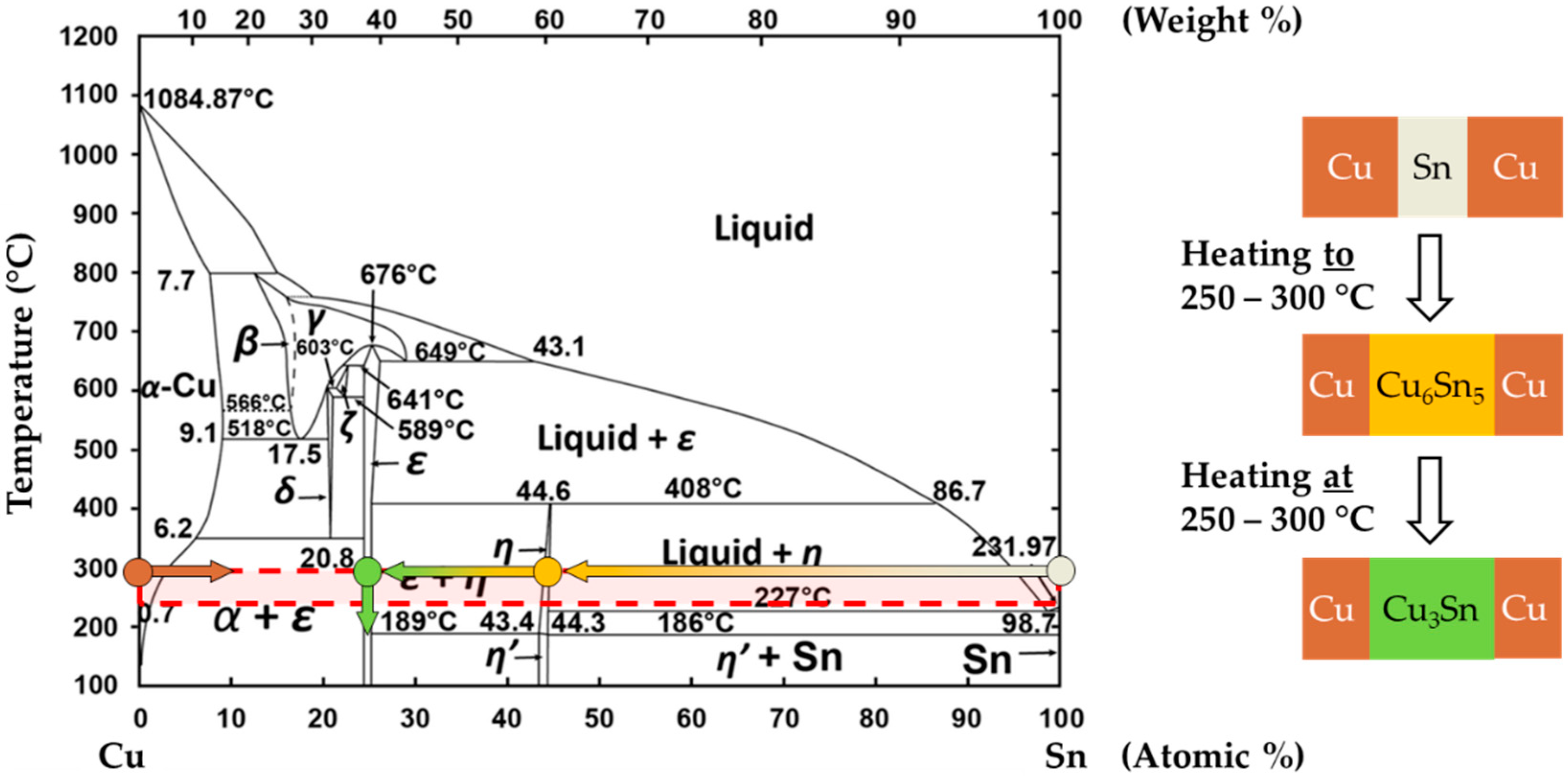
2.2. Solid-Liquid Interdiffusion Bonding
3. Experimental Setup
3.1. Design and Materials
3.2. Simulation Model
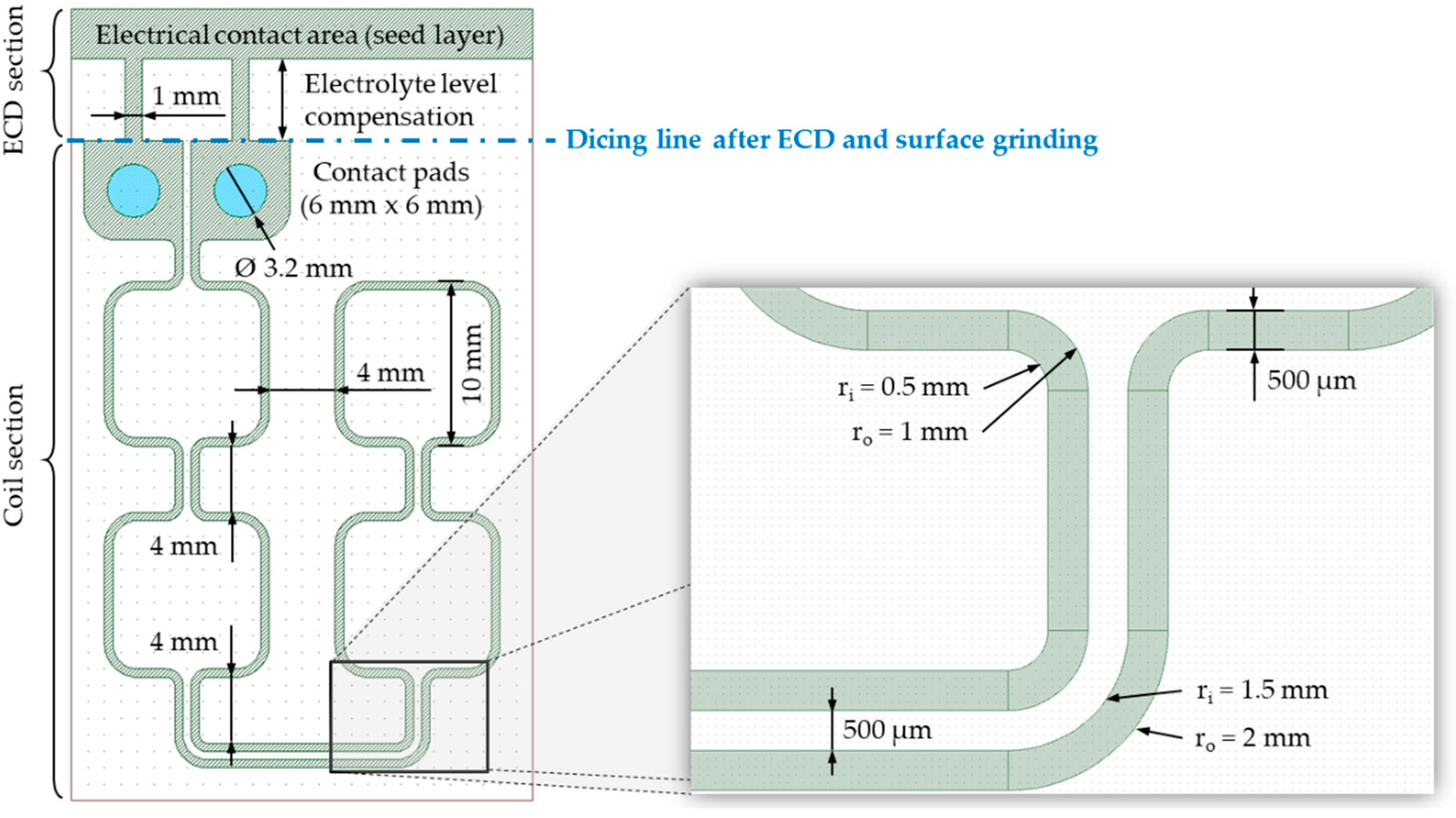
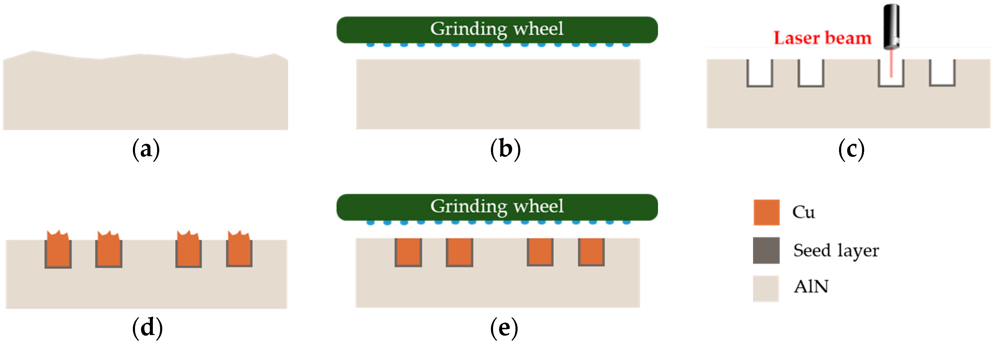
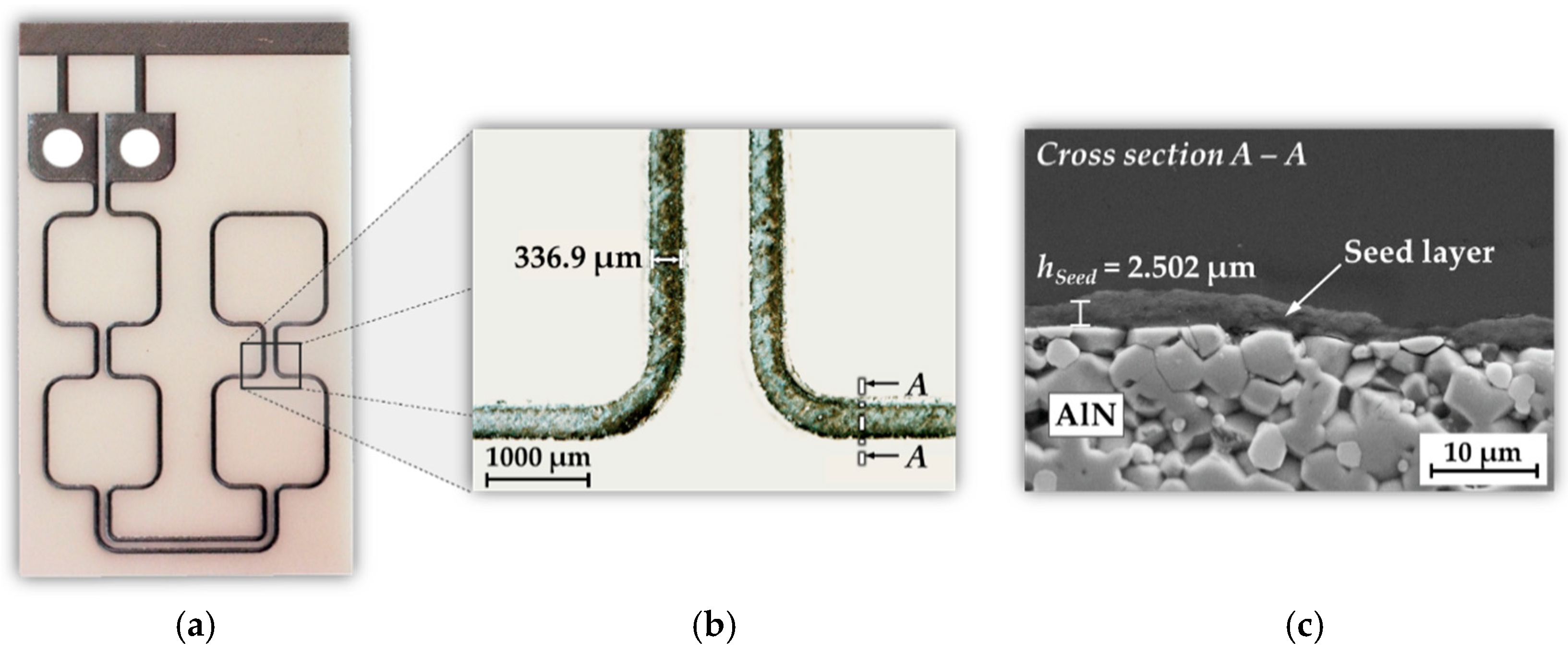
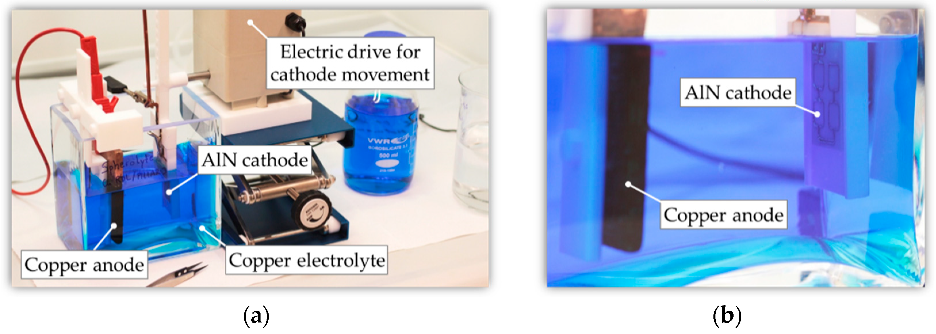
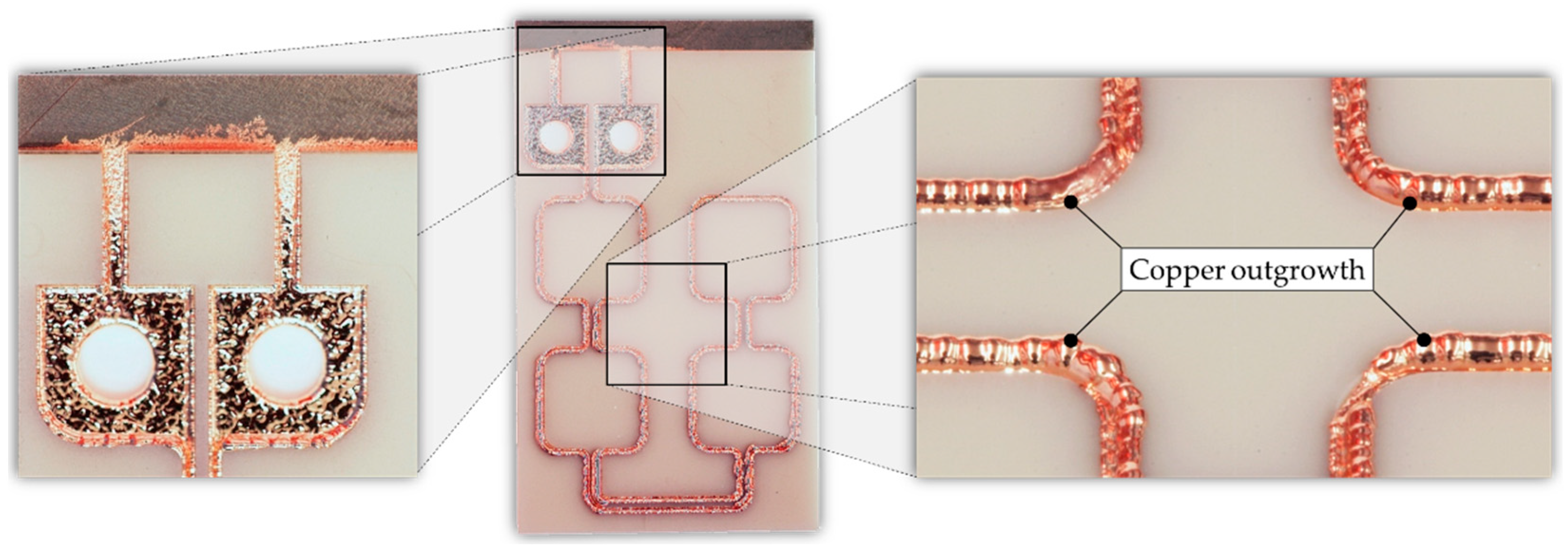
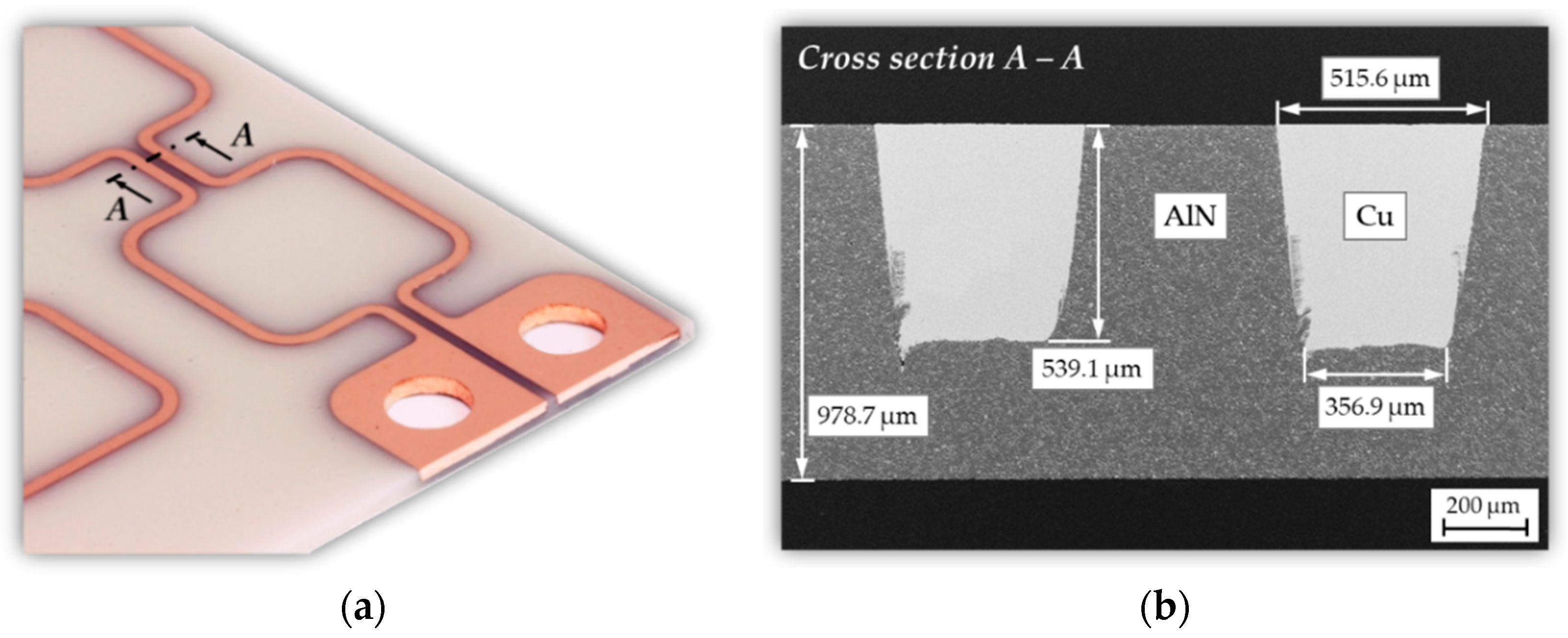
3.3. Micro Coil
- ECD section with electrically conductive contact area for electroplating as well as electrolyte level compensation;
- Coil section with conductor lines as well as contact pads for smart connectivity with the induction generator.
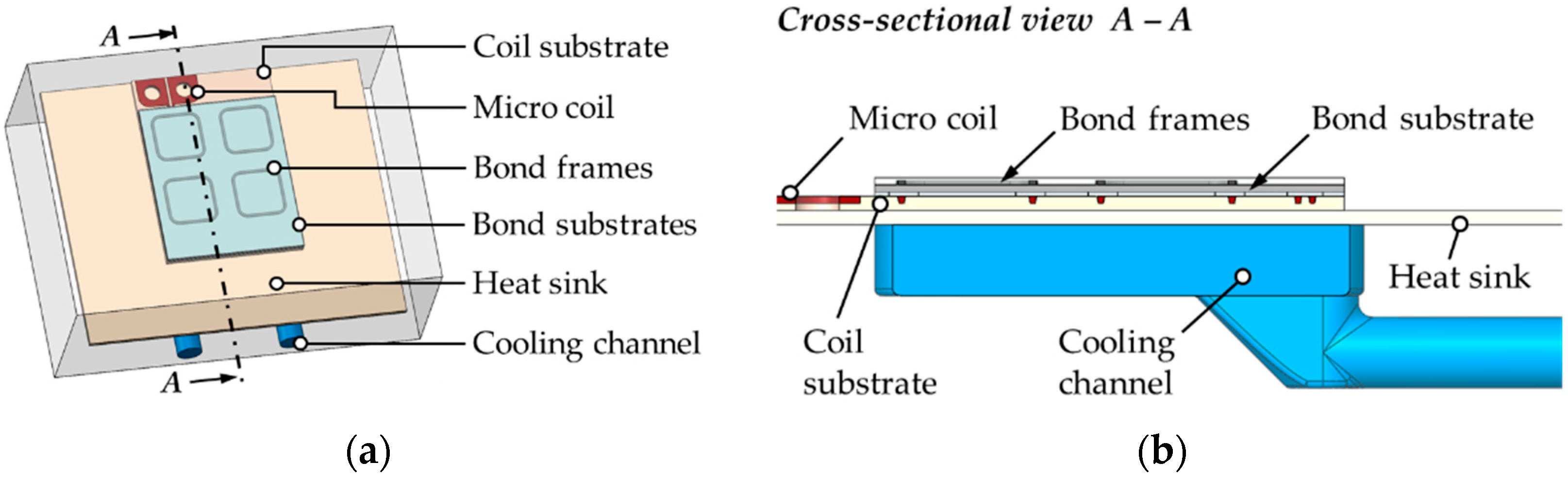
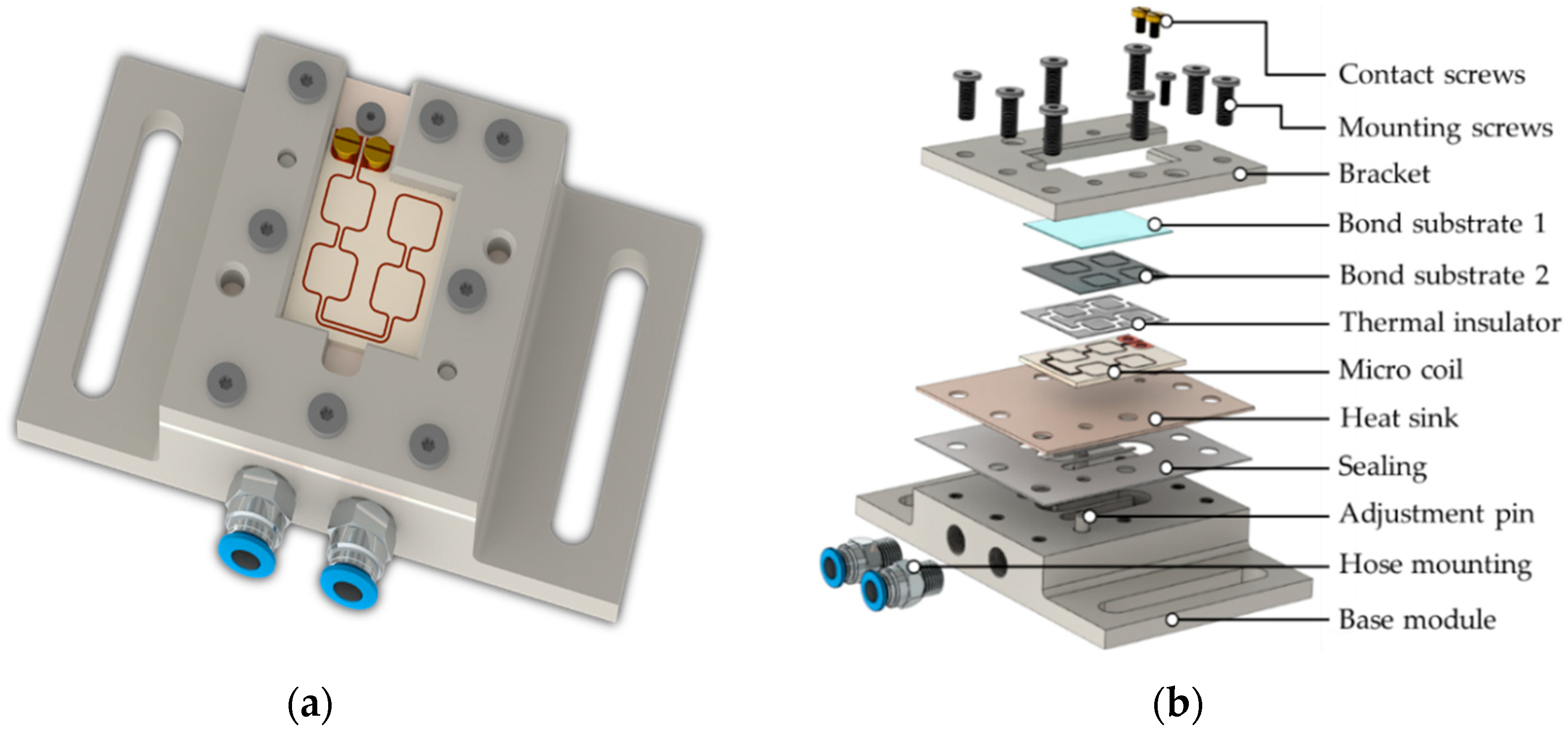
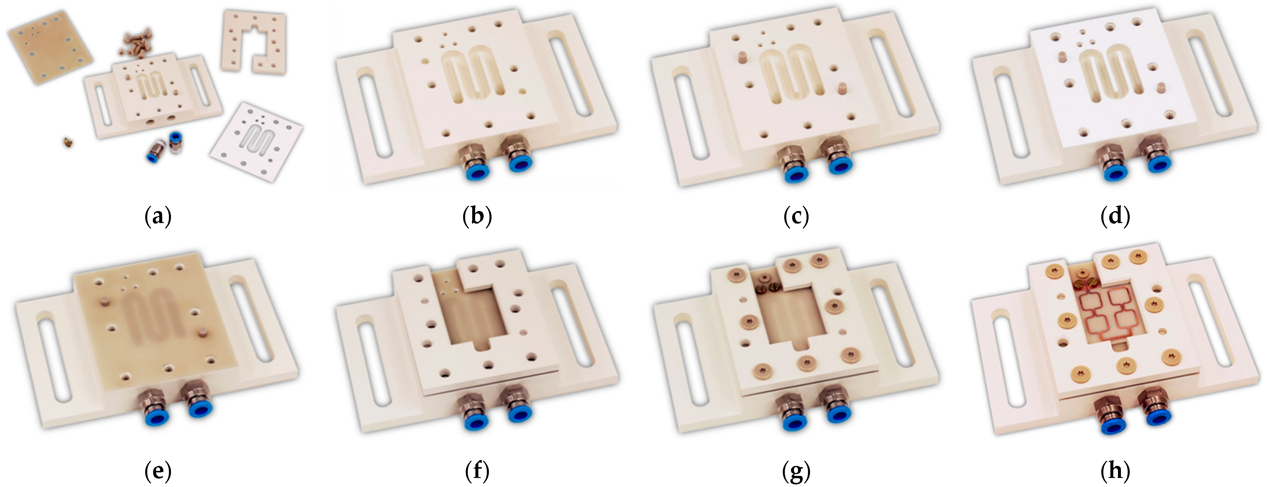
3.4. Inductive Bonding Module
- Transfer of the entire experimental setup consisting of bonding module, micro coil, and bond substrates to the inductive bonding system
- Efficient cooling of the micro coil during induction heating;
- Electrical connection of the micro coil with the induction generator;
- Alignment of the bond structures to the coil layout.
- Connection concept: releasable, mechanical screw fitting without soldering;
- Connection cable: high frequency litz wire for low electrical losses;
- Connection element/fastener: cable lug, screw.
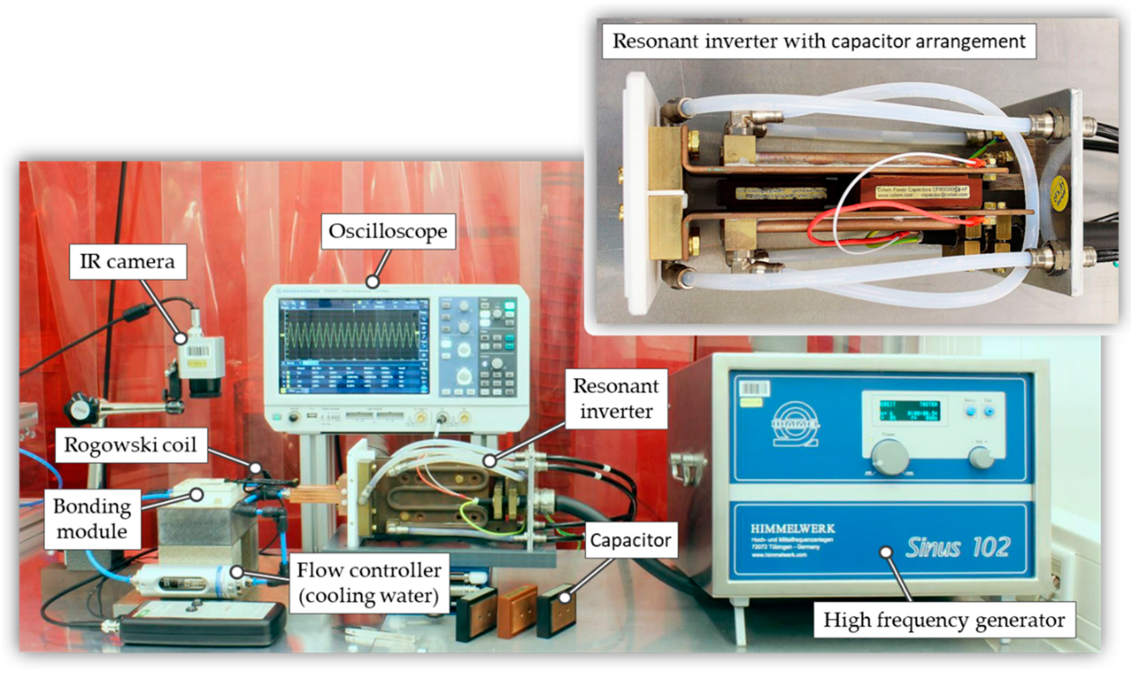
3.5. Inductive Heating System
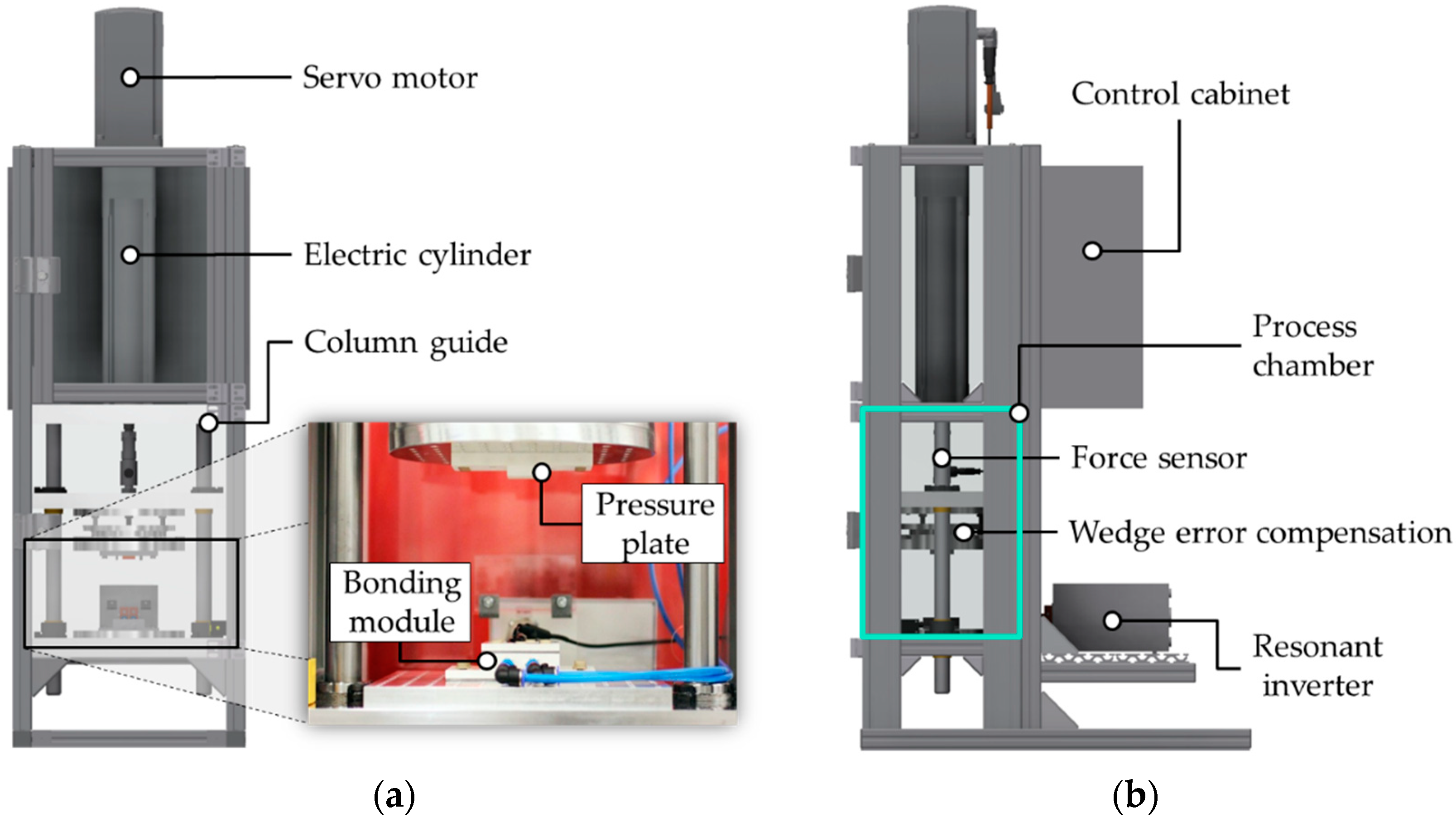
3.6. Inductive Bonding System
4. Results and Discussion
4.1. FE Simulation of Coil Geometry
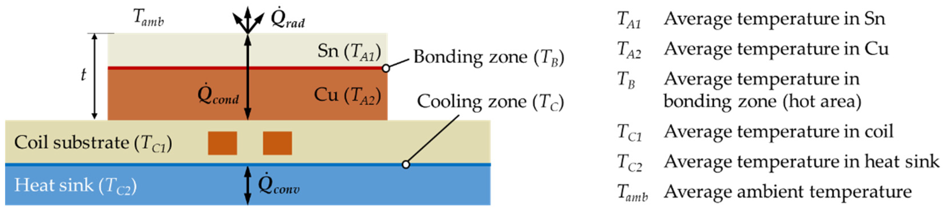
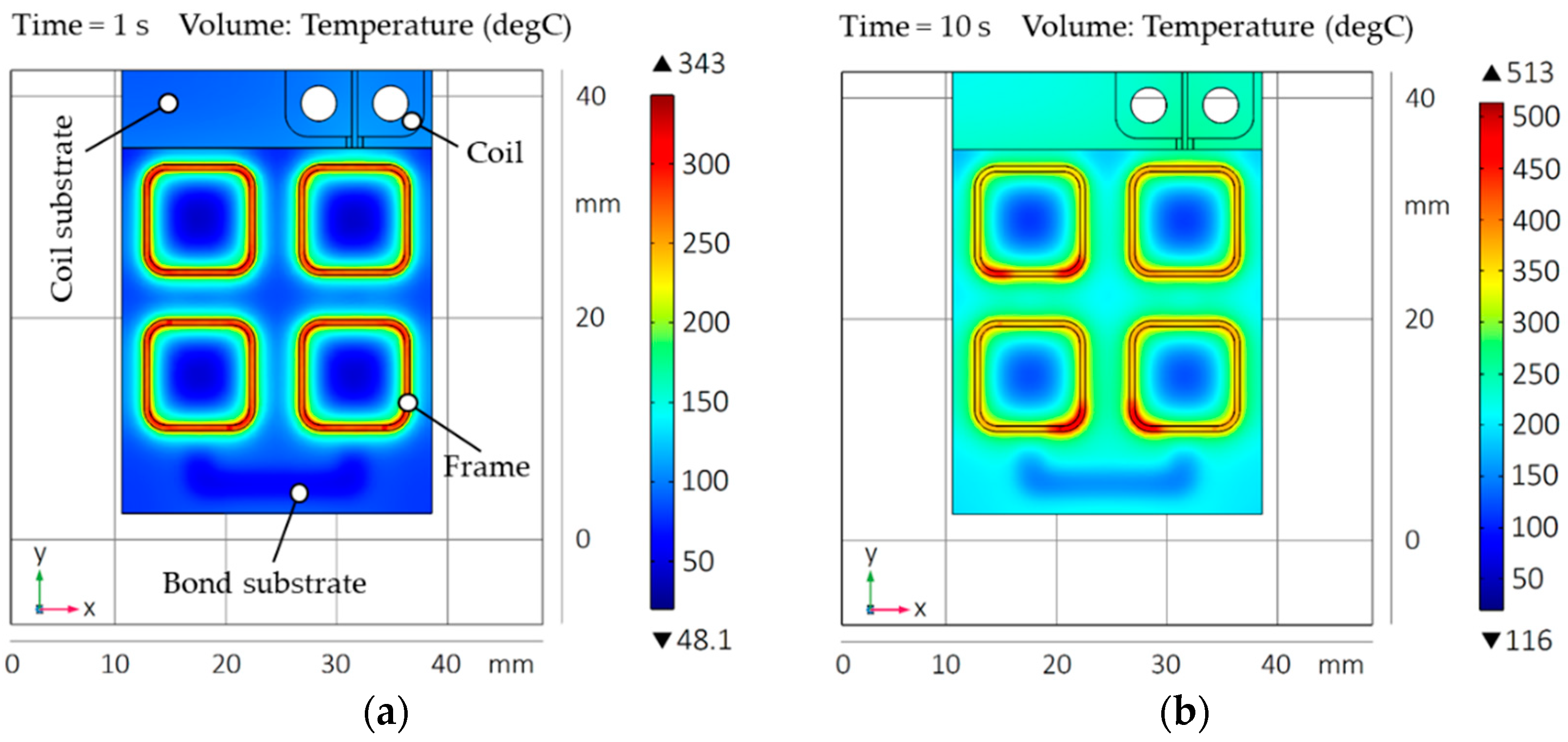
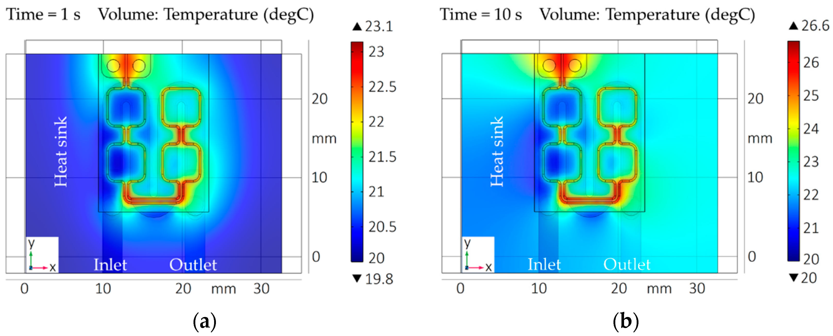
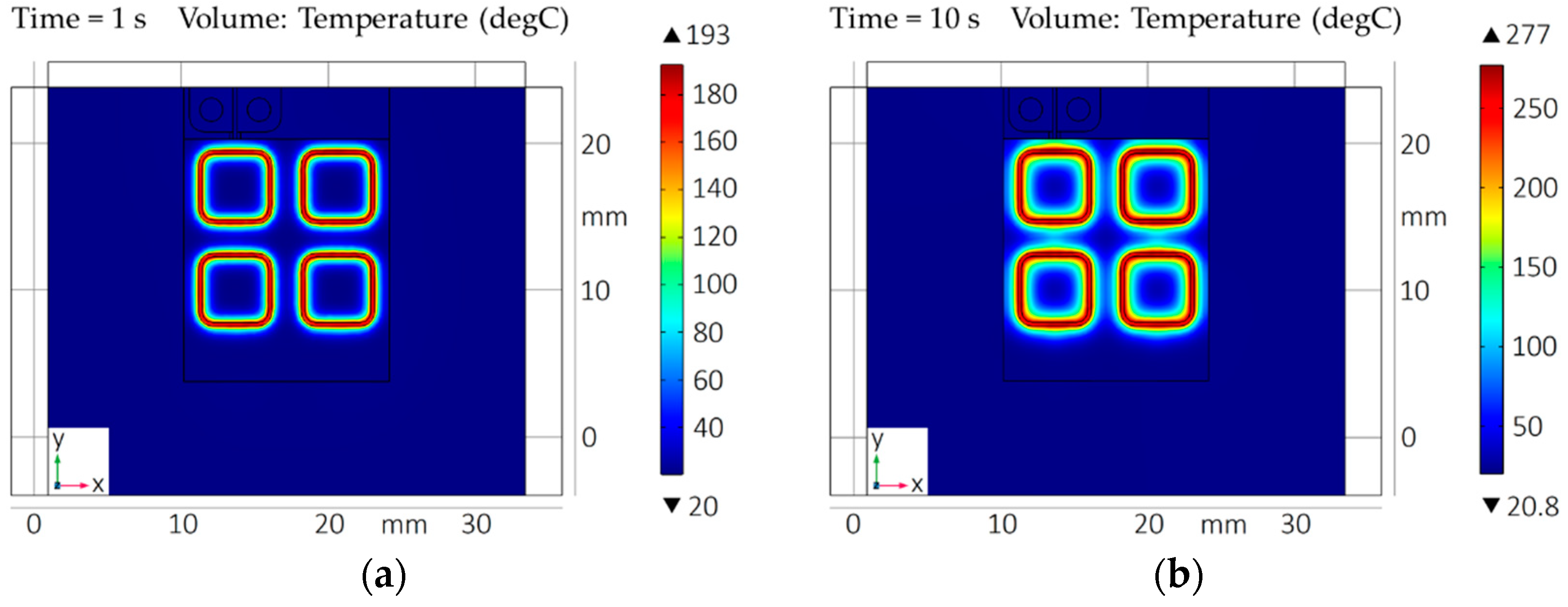
4.2. FE Simulation of Thermal Management
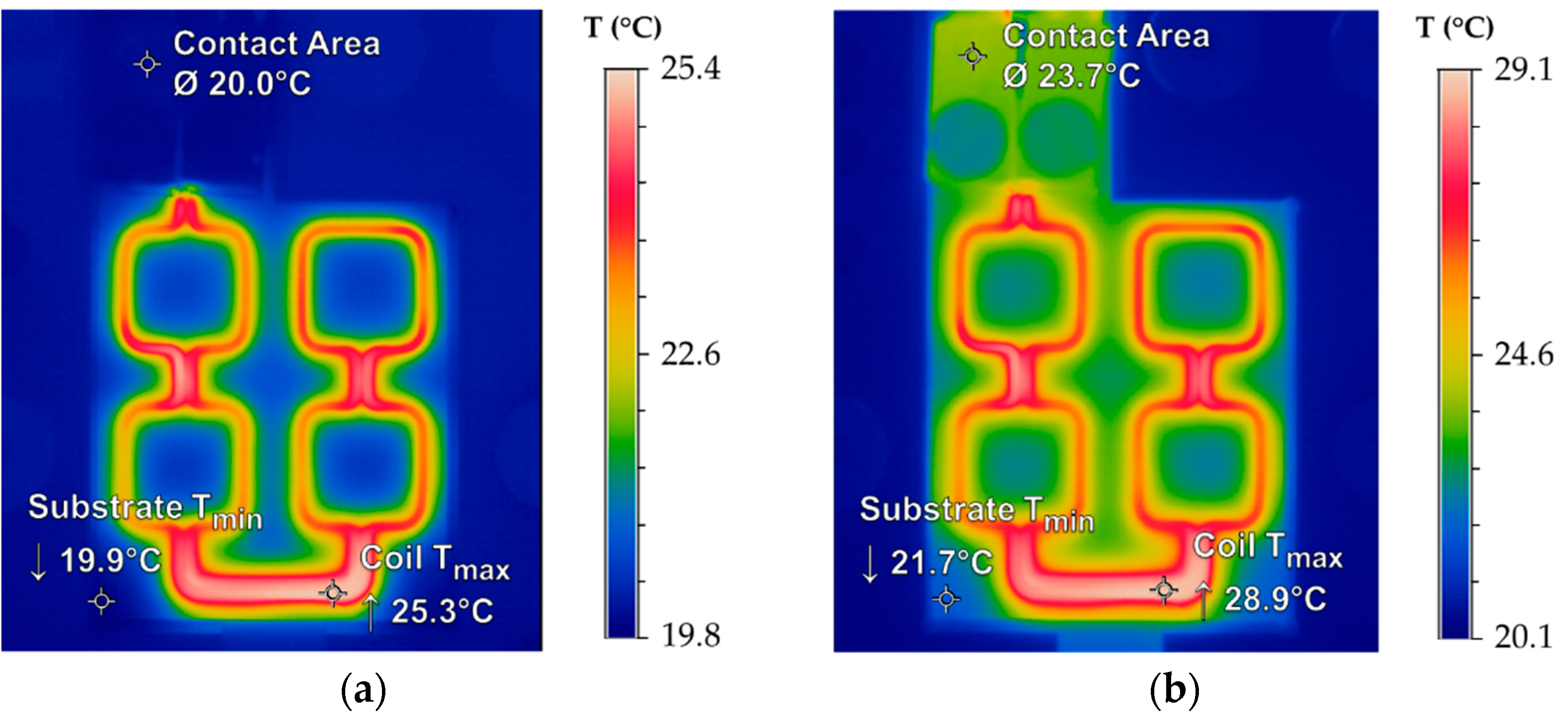
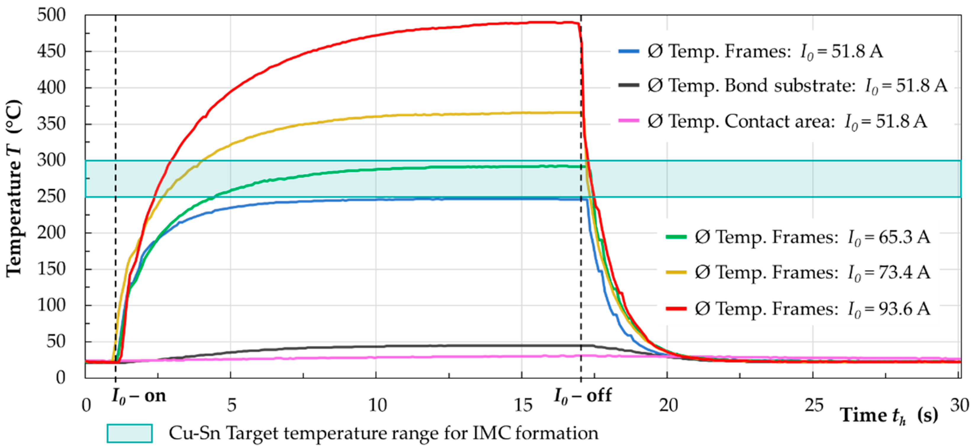
4.3. Inductive Heating
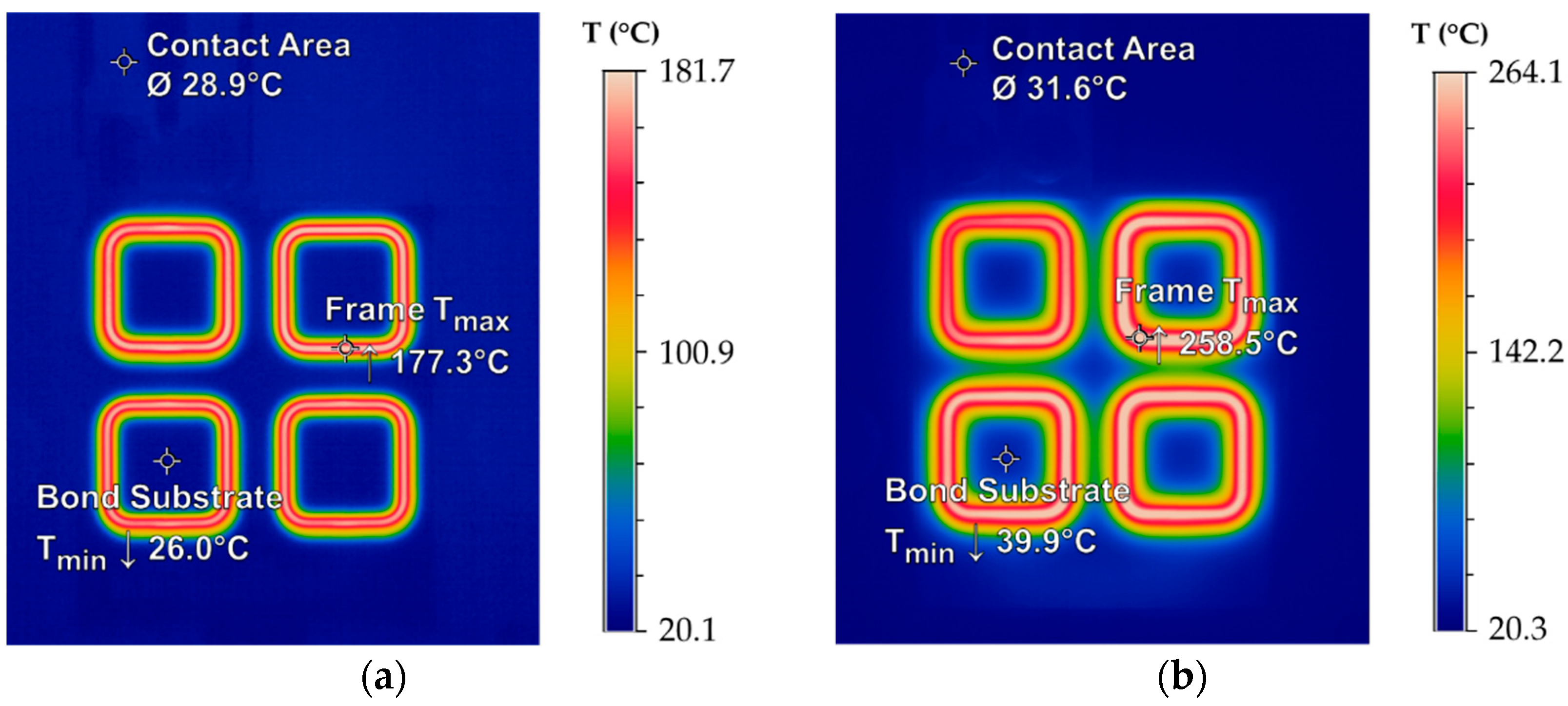
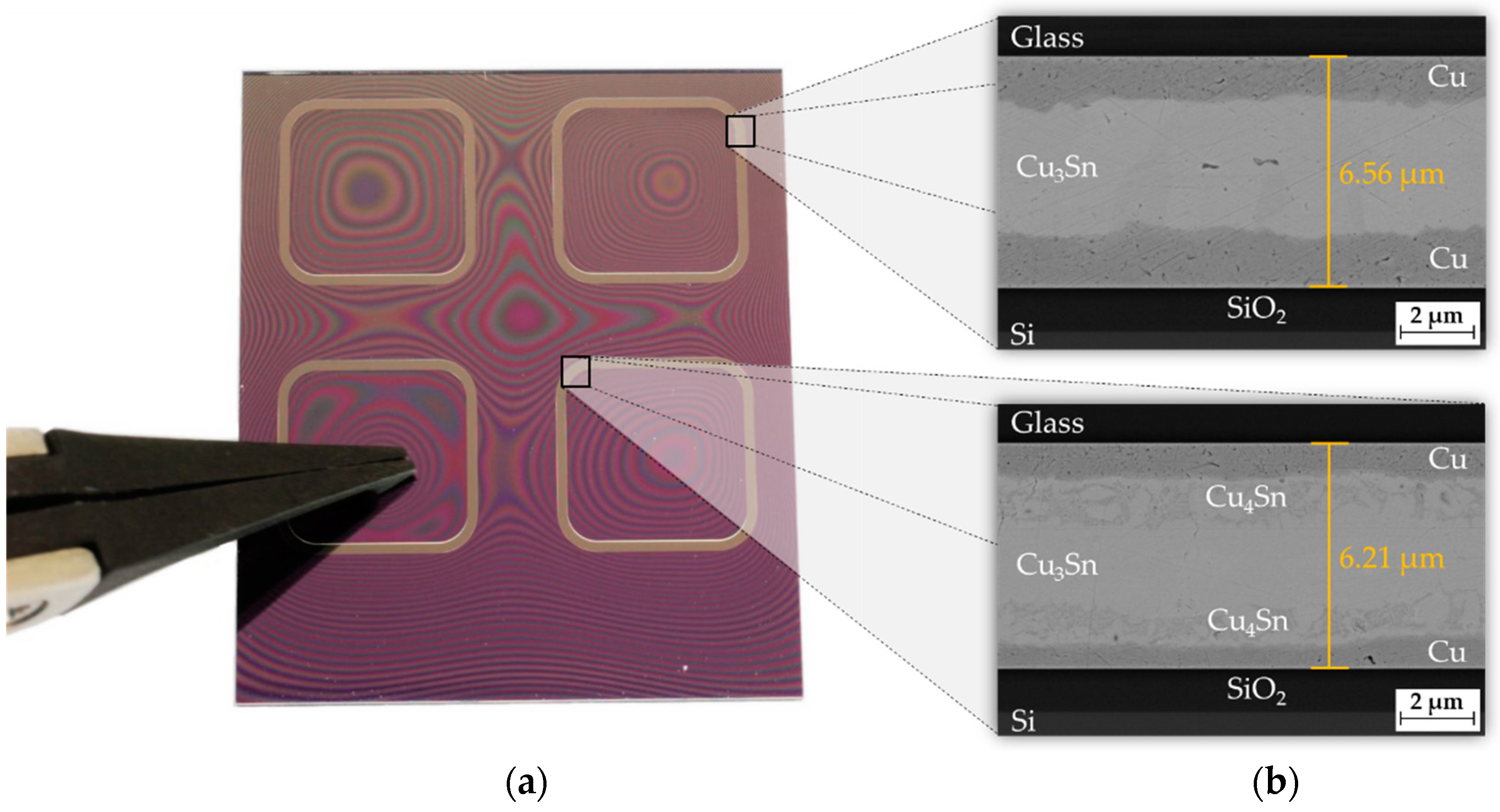
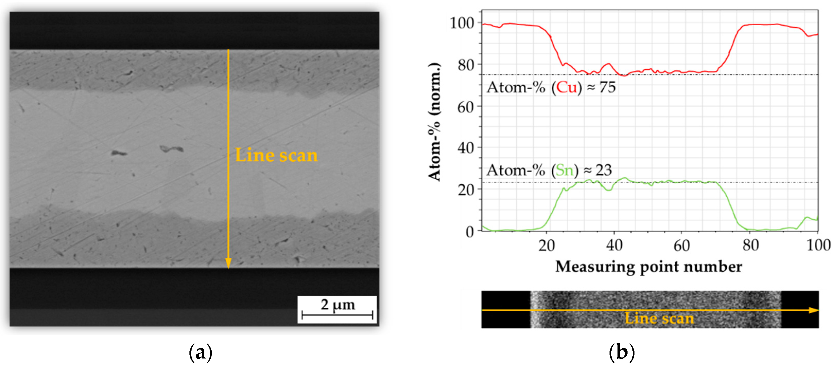
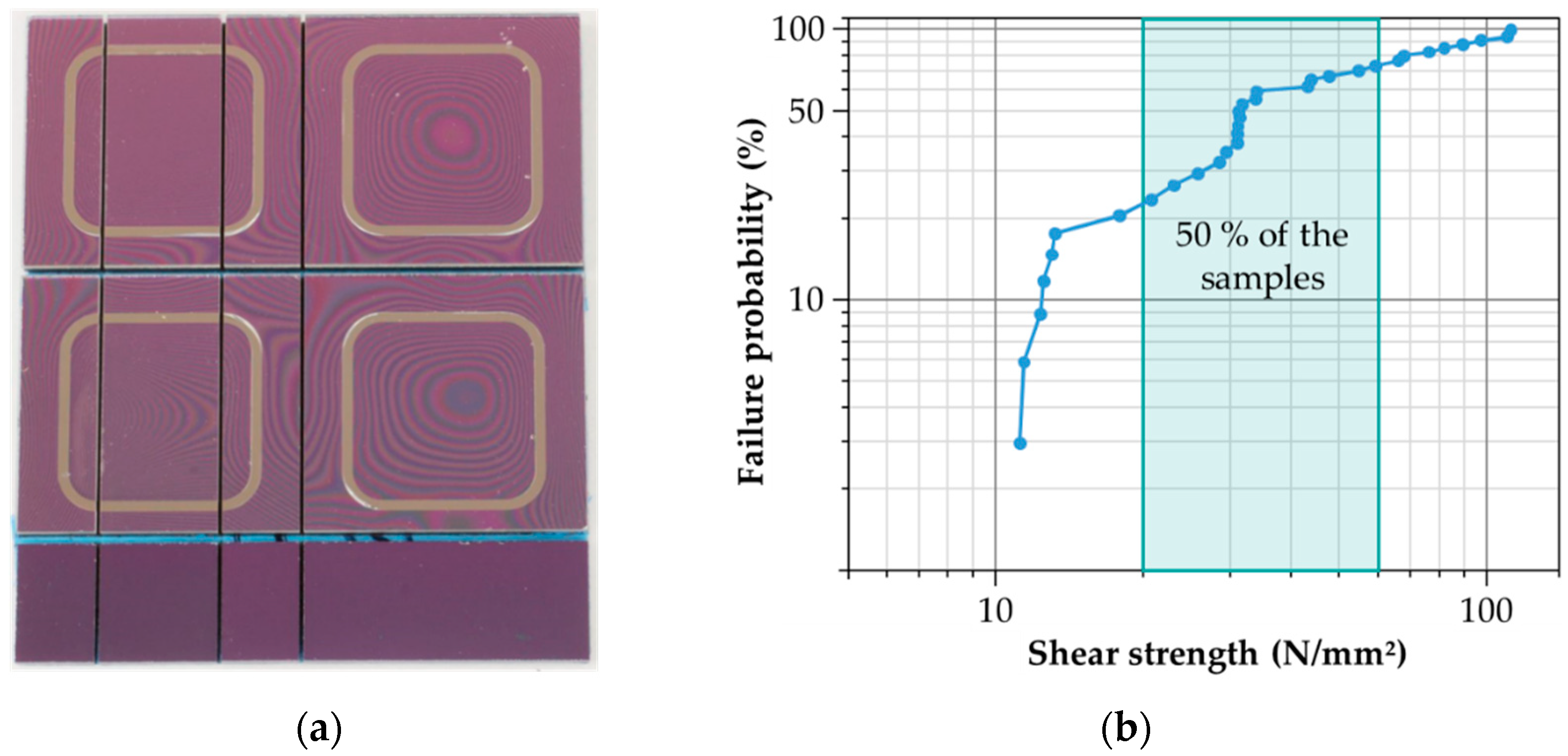
4.4. Inductive Bonding
5. Conclusions
Author Contributions
Funding
Institutional Review Board Statement
Informed Consent Statement
Data Availability Statement
Conflicts of Interest
References
- Masayoshi, E. (Ed.) Overview. In 3D and Circuit Integration of MEMS, 1st ed.; Wiley-VCH: Weinheim, Germany, 2021; pp. 309–329. ISBN 978-3-527-34647-9. [Google Scholar]
- Garrou, P.; Koyanagi, M.; Ramm, P. Handbook of 3D Integration, Volume 3: 3D Process Technology, 1st ed.; Wiley-VCH: Weinheim, Germany, 2014; ISBN 978-3-527-33466-7. [Google Scholar]
- Kim, S.E.; Kim, S. Wafer level Cu–Cu direct bonding for 3D integration. Microelectron. Eng. 2015, 137, 158–163. [Google Scholar] [CrossRef]
- Ramm, P.; Lu, J.-Q.; Taklo, M.V. Handbook of Wafer Bonding, 1st ed.; Wiley-VCH: Weinheim, Germany, 2012; ISBN 978-3-527-32646-4. [Google Scholar]
- Higurashi, E.; Suga, T. Review of low-temperature bonding technologies and their application in optoelectronic devices. Electron. Commun. Jpn. 2016, 99, 63–71. [Google Scholar] [CrossRef]
- Plach, T.; Henttinen, K.; Suni, T.; Dragoi, V. Silicon direct bonding. In Handbook of Silicon Based MEMS Materials and Technologies, 3rd ed.; Tilli, M., Paulasto-Kröckel, M., Petzold, M., Theuss, H., Motooka, T., Lindroos, V., Eds.; Elsevier Inc.: Amsterdam, The Netherlands, 2020; pp. 567–580. ISBN 978-0-323-29965-7. [Google Scholar]
- Torunbalci, M.M.; Alper, S.E.; Akin, T. Wafer level hermetic sealing of MEMS devices with vertical feedthroughs using anodic bonding. Sens. Actuator A Phys. 2015, 224, 169–176. [Google Scholar] [CrossRef]
- Knechtel, R.; Dempwolf, S.; Schikowski, M. Glass frit bonding. In Handbook of Silicon Based MEMS Materials and Technologies, 3rd ed.; Tilli, M., Paulasto-Kröckel, M., Petzold, M., Theuss, H., Motooka, T., Lindroos, V., Eds.; Elsevier Inc.: Amsterdam, The Netherlands, 2020; pp. 593–608. ISBN 978-0-323-29965-7. [Google Scholar]
- Ailas, H.; Saarilahti, J.; Pensala, T.; Kiihamäki, J. Low-temperature Cu-Cu thermocompression bonding for encapsulation of a MEMS mirror. In Proceedings of the IMAPS Nordic Conference on Microelectronics Packaging (NordPac), Copenhagen, Denmark, 11–13 June 2019. [Google Scholar]
- Malik, N.; Carvalho, P.A.; Poppe, E.; Finstad, T.G. Interfacial characterization of Al-Al thermocompression bonds. J. Appl. Phys. 2016, 119, 205303. [Google Scholar] [CrossRef]
- Ong, J.-J.; Chiu, W.-L.; Lee, O.-H.; Chiang, C.-W.; Chang, H.-H.; Wang, C.-H.; Shie, K.-C.; Yang, S.-C.; Tran, D.-P.; Tu, K.-N.; et al. Low-Temperature Cu/SiO2 Hybrid Bonding with Low Contact Resistance Using (111)-Oriented Cu Surfaces. Materials 2022, 15, 1888. [Google Scholar] [CrossRef] [PubMed]
- Huebner, H.; Penka, S.; Barchmann, B.; Eigner, M.; Gruber, W.; Nobis, M.; Janka, S.; Kristen, G.; Schneegans, M. Microcontacts with sub-30 μm pitch for 3D chip-on-chip integration. Microelectron. Eng. 2006, 83, 2155–2162. [Google Scholar] [CrossRef]
- Honrao, C.; Huang, T.-C.; Kobayashi, M.; Smet, V.; Raj, P.M.; Tummala, R. Accelerated SLID bonding using thin multi-layer copper-solder stack for fine-pitch interconnections. In Proceedings of the IEEE 64th Electronic Components and Technology Conference (ECTC), Orlando, FL, USA, 27–30 May 2014. [Google Scholar]
- Luu, T.T. Solid Liquid Interdiffusion Wafer-Level Bonding for MEMS Packaging. Ph.D. Thesis, Buskerud and Vestfold University College (HBV), Horten, Norway, 2015. [Google Scholar]
- Hilton, A.; Temple, D.S. Wafer-Level Vacuum Packaging of Smart Sensors. Sensors 2016, 16, 1819. [Google Scholar] [CrossRef] [PubMed]
- Bernstein, L. Semiconductor joining by solid-liquid-interdiffusion (SLID) process. J. Electrochem. Soc. 1966, 113, 1282–1288. [Google Scholar] [CrossRef]
- Manh, T.; Nguyen, H.-V.; Le-Anh, D.; Aasmundtveit, K.E.; Hoff, L.; Eggen, T.; Johansen, T.F.; Lanteri, F.; Gelly, J.-F. Au-Sn Solid-Liquid Interdiffusion (SLID) bonding for piezoelectric ultrasonic transducers. In Proceedings of the IEEE International Ultrasonics Symposium (IUS), Tours, France, 18–21 September 2016. [Google Scholar]
- Aasmundtveit, K.E.; Tekseth, K.R.; Breiby, D.W.; Nguyen, H.-V. High-energy X-ray Tomography for 3D Void Characterization in Au–Sn Solid-Liquid Interdiffusion (SLID) Bonds. In Proceedings of the 22nd European Microelectronics and Packaging Conference & Exhibition (EMPC), Pisa, Italy, 16–19 June 2019. [Google Scholar]
- Luu, T.T.; Duan, A.; Aasmundtveit, K.E.; Hoivik, N. Optimized Cu-Sn Wafer-Level Bonding Using Intermetallic Phase Characterization. J. Electron. Mater. 2013, 42, 3582–3592. [Google Scholar] [CrossRef]
- Aasmundtveit, K.E.; Luu, T.; Wang, K.; Hoivik, N. Void formation in Cu-Sn Solid-Liquid Interdiffusion (SLID) bonding. In Proceedings of the European Microelectronics Packaging Conference (EMPC), Friedrichshafen, Germany, 14–16 September 2015. [Google Scholar]
- Goldschmidt, H. Verfahren zur Herstellung von Metallen Oder Metalloiden Oder Legierungen Derselben. Patent Deutsches Reich 96317, 13 March 1895. [Google Scholar]
- Clevenger, L.A.; Thompson, C.V.; Cammarata, R.C.; Tu, K.N. Reaction kinectics of nickel/silicon multilayer films. Appl. Phys. Lett. 1988, 52, 795–797. [Google Scholar] [CrossRef]
- Braeuer, J. Erarbeitung Eines Raumtemperatur-Waferbondverfahrens Basierend auf Integrierten und Reaktiven Nanoskaligen Multilagensystemen. Ph.D. Thesis, Chemnitz University of Technology, Chemnitz, Germany, 2014. [Google Scholar]
- Braeuer, J.; Besser, J.; Wiemer, M.; Gessner, T. A novel technique for MEMS packaging: Reactive bonding with integrated material systems. Sens. Actuator A Phys. 2012, 188, 212–219. [Google Scholar] [CrossRef]
- Braeuer, J.; Gessner, T. A hermetic and room-temperature wafer bonding technique based on integrated reactive multilayer systems. J. Micromech. Microeng. 2014, 24, 115002. [Google Scholar] [CrossRef]
- Vogel, K.; Roscher, F.; Wiemer, M.; Zimmermann, S.; Otto, T. Reactive bonding with oxide based reactive multilayers. In Proceedings of the Smart Systems Integration (SSI), Dresden, Germany, 11–12 April 2018. [Google Scholar]
- Wiemer, M.; Hofmann, C.; Vogel, K. Selective heat input for low temperature metallic wafer level bonding. In Proceedings of the PRiME, ECS Transactions, Digital Meeting, 4–9 October 2020. [Google Scholar]
- Vogel, K.; Braun, S.; Hofmann, C.; Weiser, M.; Wiemer, M.; Otto, T.; Kuhn, H. Reactive Bonding. In 3D and Circuit Integration of MEMS, 1st ed.; Masayoshi, E., Ed.; Wiley-VCH: Weinheim, Germany, 2021; pp. 309–329. ISBN 978-3-527-34647-9. [Google Scholar]
- Benkowsky, G. Induktionserwaermung: Haerten, Gluehen, Schmelzen, Loeten, Schweissen, 5th ed.; Verlag Technik: Berlin, Germany, 1990; ISBN 978-3-341-00813-3. [Google Scholar]
- Rudnev, V.; Loveless, D.; Cook, R.L. Handbook of Induction Heating, 2nd ed.; Crc Press Inc.: Boca Raton, GL, USA, 2017; ISBN 978-1-4665-5395-8. [Google Scholar]
- Kraeusel, V.; Froehlich, A.; Kroll, M.; Rochala, P.; Kimme, J.; Wertheim, R. A highly efficient hybrid inductive joining technology for metals and composites. CIRP Ann.-Manuf. Technol. 2018, 67, 5–8. [Google Scholar] [CrossRef]
- Froehlich, A.; Rochala, P.; Matthess, D.; Kraeusel, V. A Sustainable Hybrid Inductive Joining Technology for Aluminum and Composites. Procedia Manuf. 2019, 35, 143–148. [Google Scholar] [CrossRef]
- Kroll, M.; Birnbaum, P.; Zeisig, J.; Kraeusel, V.; Wagner, M.F.-X. Manufacturing of 42SiCr-Pipes for Quenching and Partitioning by Longitudinal HFI-Welding. Metals 2019, 9, 716. [Google Scholar] [CrossRef]
- Egger, C.; Kroll, M.; Kern, K.; Steimer, Y.; Schreiner, M.; Tillmann, W. Experimental Investigation of Temperature and Contact Pressure Influence on HFI Welded Joint Properties. Materials 2022, 15, 3615. [Google Scholar] [CrossRef] [PubMed]
- Thompson, K.; Gianchandani, Y.B.; Booske, J.; Cooper, R.F. Direct silicon-silicon bonding by electromagnetic induction heating. J. Microelectromech. Syst. 2022, 11, 285–292. [Google Scholar] [CrossRef]
- Yang, H.; Wu, M.; Fang, W. Integration of the fabrication processes and wafer level packaging of MEMS devices using localized induction heating. In Proceedings of the IEEE/LEOS International Conference on Optical MEMS, Waikoloa, HI, USA, 18–21 August 2003. [Google Scholar]
- Yang, H.-A.; Wu, M.; Fang, W. Localized induction heating solder bonding for wafer level MEMS packaging. J. Micromech. Microeng. 2004, 15, 394–399. [Google Scholar] [CrossRef]
- Chen, M.; Liu, W.; Xi, Y.; Lin, C.; Wong, C.P.; Liu, S. Selective induction heating for wafer level bonding and packaging. In Proceedings of the 59th Electronic Components and Technology Conference (ECTC), San Diego, CA, USA, 26–29 May 2009. [Google Scholar]
- Hofmann, C.; Froehlich, A.; Kimme, J.; Wiemer, M.; Otto, T. A Novel Method for Mems Wafer-Level Packaging: Selective and Rapid Induction Heating for Copper-Tin SLID Bonding. In Proceedings of the 20th International Conference on Solid-State Sensors, Actuators and Microsystems & Eurosensors XXXIII (TRANSDUCERS & EUROSENSORS XXXIII), Berlin, Germany, 23–27 June 2019. [Google Scholar]
- Yin, Z.; Sun, F.; Guo, M. The fast formation of Cu-Sn intermetallic compound in Cu/Sn/Cu system by induction heating process. Mater. Lett. 2018, 215, 207–210. [Google Scholar] [CrossRef]
- Sun, F.; Zuozhu, Y. The interfacial Cu–Sn intermetallic compounds (IMCs) growth behavior of Cu/Sn/Cu sandwich structure via induction heating method. J. Mater. Sci. Mater. Electron. 2019, 30, 18878–18884. [Google Scholar] [CrossRef]
- Hammad, A.E.; El-Molla, S.; Abd El-Rehim, A.F.; Ragab, M. Progress on microstructure features and creep properties of prospective Tin-Silver-Zinc alloy using a magnetic field. Mater. Res. Express 2021, 8, 086506. [Google Scholar] [CrossRef]
- Hofmann, C.; Baum, M.; Satwara, M.; Kroll, M.; Panhale, S.; Rochala, P.; Paul, S.-D.; Oi, K.; Murayama, K.; Wiemer, M.; et al. Silver sintering technology based on induction heating for chip level bonding. In Proceedings of the IEEE CPMT Symposium Japan (ICSJ), Kyoto, Japan, 10–12 November 2021. [Google Scholar]
- Nasir, B.A. Current Density Distribution in a Cylindrical Workpiece of Traveling Wave Induction Heaters. Eng. Technol. 2002, 21, 1–10. [Google Scholar]
- Goldstein, R.; Stuehr, W.; Bleck, M. Design and Fabrication of Inductors for Induction Heat Treating. In ASM Handbook, 4th ed.; Rudnev, V., Totten, G.E., Eds.; ASM International: Almere, The Netherlands, 2014; pp. 589–606. ISBN 978-1-62708-012-5. [Google Scholar]
- Chaki, C.; Chaki, M.; Roy, K. Development of a Simplistic Method to Simulate the Formation of Intermetallic Compounds in Diffusion Soldering Process. Am. J. Mater. Synth. Process. 2019, 4, 54–61. [Google Scholar] [CrossRef]
- Xu, H.; Suni, T.; Vuorinen, V.; Li, J. Wafer-level SLID bonding for MEMS encapsulation. Adv. Manuf. 2013, 1, 226–235. [Google Scholar] [CrossRef]
- Sanabria, C. A New Understanding of the Heat Treatment of Nb3Sn Superconducting Wires. Ph.D. Thesis, The Florida State University, Tallahassee, FL, USA, 2017. [Google Scholar]
- Hao, Z.; Zhichao, L.; Lilin, T.; Zhimin, T.; Litian, L.; Zhijian, L. Thermal conductivity measurements of ultra-thin single crystal silicon films using improved structure. In Proceedings of the 8th International Conference on Solid-State and Integrated Circuit Technology (ICSICT), Shanghai, China, 23–26 October 2006. [Google Scholar]
- Jain, A.; McGaughey, A. Effect of exchange–correlation on first-principles-driven lattice thermal conductivity predictions of crystalline silicon. Comput. Mater. Sci. 2015, 110, 115–120. [Google Scholar] [CrossRef]
- Edwards, T.C.; Steer, M.B. Foundations for Microstrip Circuit Design, 4th ed.; Wiley-IEEE Press: Hoboken, NJ, USA, 2016; ISBN 978-1-118-93619-1. [Google Scholar]
- Alunit®—The Cool Solution for Electronic Power. Available online: https://www.ceramtec.com.cn/files/el_alunit-the-cool-solution-for-electronic-power.pdf (accessed on 14 June 2022).
- Webster, J.G. (Ed.) Electrical Conductivity and Resistivity. In Electrical Measurement, Signal Processing, and Displays, 1st ed.; CRC Press: Boca Raton, FL, USA, 2003; pp. 7-1–7-14. ISBN 978-0849317330. [Google Scholar]
- Vogel, K.; Haubold, M.; Wiemer, M.; Gessner, T. Overview of Wafer Bonding and Characterization of the Bonded Interface. In Smart Systems Integration for Micro- and Nanotechnologies, 1st ed.; Michel, B., Otto, T., Schulz, S.E., Winkler, T., Eds.; Goldenbogen: Dresden, Germany, 2014; pp. 473–481. ISBN 978-3-932434-78-5. [Google Scholar]
- Aasmundtveit, K.E.; Luu, T.-T.; Vardøy, A.-S.B.; Tollefsen, T.A.; Wang, K.; Hoivik, N. High-temperature shear strength of solid-liquid interdiffusion (SLID) bonding: Cu-Sn, Au-Sn and Au-In. In Proceedings of the 5th Electronics System-integration Technology Conference (ESTC), Helsinki, Finland, 16–18 September 2014. [Google Scholar]


| Symbol | Unit | Parameter Range | |||||
|---|---|---|---|---|---|---|---|
| Frequency | f | MHz | 1.00 | 1.25 | 1.50 | 1.75 | 2.00 |
| Copper | |||||||
| Skin depth @ 25 °C | δ | µm | 67.26 | 60.16 | 54.92 | 50.84 | 47.56 |
| Tin | |||||||
| Skin depth @ 25 °C | δ | µm | 166.9 | 149.28 | 136.27 | 126.16 | 118.02 |
| Symbol 1 | Unit | Parameter | |
|---|---|---|---|
| Dimensions | |||
| Length | l | mm | 33 |
| Width | w | mm | 28 |
| Silicon substrate | |||
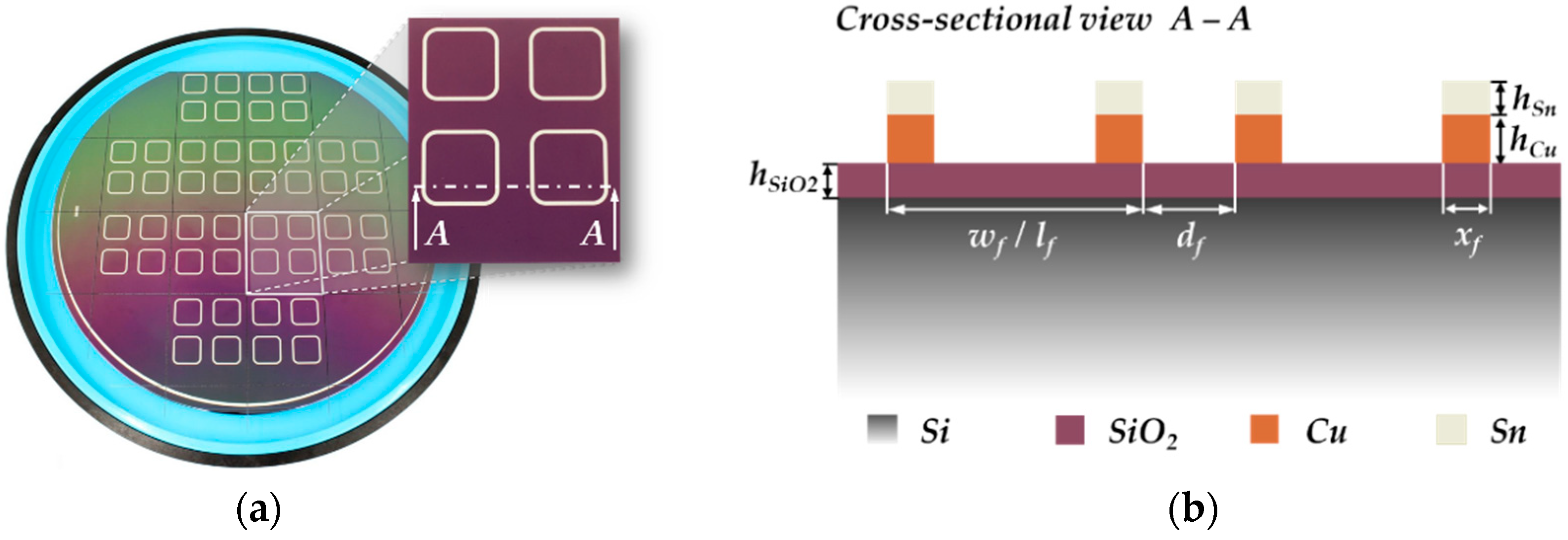
| Thickness | hSi | µm | 675 |
| Thermal conductivity | λSi | W/(m·K) | 153 [49,50] |
| Volume resistivity | ρSi | Ω·cm | 10 to 20 |
| Thickness of thermal barrier (SiO2) | hSiO2 | µm | 2 |
| Borofloat® 33 substrate | |||
| Thickness | hG | µm | 500 |
| Thermal conductivity | λG | W/(m·K) | 1.2 [51] |
| Volume resistivity | ρG | Ω·cm | 1 × 10⁸ (at 250 °C) [51] |
| Symbol 1 | Unit | Parameter | |
|---|---|---|---|
| Length | lf | mm | 10 |
| Width | wf | mm | 10 |
| Number of frames | # | – | 4 |
| Thickness copper | hCu | µm | 2.5 |
| Thickness tin | hSn | µm | 1.0 |
| Lateral frame distance | df | mm | 4 |
| Lateral frame width | xf | µm | 500 |
| Frame radius | rf | mm | 1.5 |
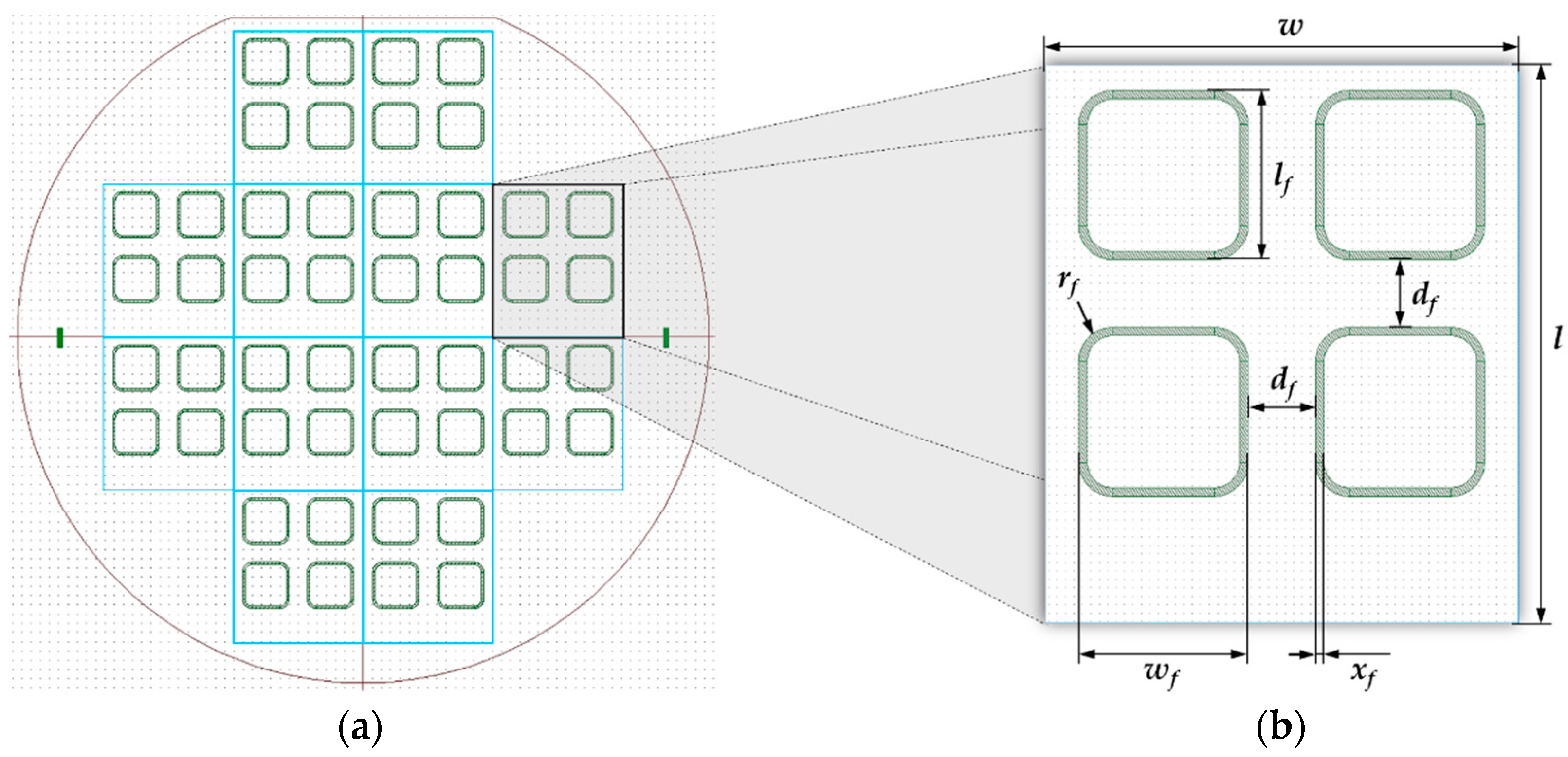
| Total frame area | Af | mm2 | 1469.2 |
| Symbol | Unit | Parameter | |
|---|---|---|---|
| Substrate parameter | |||
| Length | l | mm | 48 |
| Width | w | mm | 28 |
| Thickness | h | mm | 1 |
| Surface quality | – | – | as fired |
| Surface roughness | Ra_max | µm | 0.6 |
| Flatness | % | 0.3 | |
| Material parameter | |||
| Thermal conductivity | λ | W/(m·K) | 170 [52] |
| Specific heat capacity | cp | J/(kg·K) | 720 @ 100 °C [52] |
| Volume resistivity | ρ | Ω·cm | 1 × 10¹⁴ @ 20 °C [52] |
| Dielectric strength | κ | kV/mm | 15 @ 0.635 mm [52] |
Publisher’s Note: MDPI stays neutral with regard to jurisdictional claims in published maps and institutional affiliations. |
© 2022 by the authors. Licensee MDPI, Basel, Switzerland. This article is an open access article distributed under the terms and conditions of the Creative Commons Attribution (CC BY) license (https://creativecommons.org/licenses/by/4.0/).
Share and Cite
Hofmann, C.; Satwara, M.; Kroll, M.; Panhale, S.; Rochala, P.; Wiemer, M.; Hiller, K.; Kuhn, H. Localized Induction Heating of Cu-Sn Layers for Rapid Solid-Liquid Interdiffusion Bonding Based on Miniaturized Coils. Micromachines 2022, 13, 1307. https://doi.org/10.3390/mi13081307
Hofmann C, Satwara M, Kroll M, Panhale S, Rochala P, Wiemer M, Hiller K, Kuhn H. Localized Induction Heating of Cu-Sn Layers for Rapid Solid-Liquid Interdiffusion Bonding Based on Miniaturized Coils. Micromachines. 2022; 13(8):1307. https://doi.org/10.3390/mi13081307
Chicago/Turabian StyleHofmann, Christian, Maulik Satwara, Martin Kroll, Sushant Panhale, Patrick Rochala, Maik Wiemer, Karla Hiller, and Harald Kuhn. 2022. "Localized Induction Heating of Cu-Sn Layers for Rapid Solid-Liquid Interdiffusion Bonding Based on Miniaturized Coils" Micromachines 13, no. 8: 1307. https://doi.org/10.3390/mi13081307