
Carbon-Related Materials: Graphene and Carbon Nanotubes in Semiconductor Applications and Design

 ,
,
Abstract
:1. Introduction
2. Physical Structures
2.1. Tight-Binding Approximation
2.2. Graphene Band Structure
2.3. From Graphene to Nanotubes
2.4. Bandgap
3. Electrical and Material Properties
3.1. Semi-Metal Characteristics
3.2. Electrical Conductivity and Ballistic Transport
3.3. Melting Point and Stability
3.4. High Transparency
3.5. Thermal Conductivity
4. Growth and Transfer of Graphene
4.1. Top-Down Method
4.1.1. Exfoliation
4.1.2. Reduction
Pyrolysis
Reduction with Graphite Oxide
4.1.3. Others
4.2. Bottom-Up Method
4.2.1. Epitaxial Method
4.2.2. Chemical Vapor Deposition Method
4.3. Graphene Film Transfer
5. Growth and Mechanisms of CNTs
5.1. Growth
5.1.1. Arc-Discharge
5.1.2. Laser Ablation
5.1.3. CVD
5.1.4. Other Methods
5.2. Growth Mechanisms
5.2.1. Tip-Growth Model
5.2.2. Base-Growth Model
6. Characterizations
6.1. AFM
6.2. TEM
6.3. Raman Spectroscopy
6.4. Rayleigh Spectroscopy
6.5. XRD
7. Graphene Applications
7.1. Graphene FET
7.2. Light-Emitting Device
7.3. Energy Storage/Conversion Devices
7.3.1. As the Window Electrode
7.3.2. As an Acceptor
7.3.3. Photo-Thermoelectric Effect
7.4. Reconfigurable Multi-Function Logic
7.5. Graphene Biosensors
7.5.1. Graphene Bio-FETs
7.5.2. Impedance Biosensors
7.5.3. Electrochemiluminescence Biosensors
7.6. Graphene Optoelectronics Applications
7.6.1. Graphene Photodetector
7.6.2. CMOS-Compatible Graphene Photodetector
7.6.3. Graphene-on-Graphene Modulator
7.7. Graphene Photo Memtransistor
7.8. Other Applications
8. Applications of CNTs
8.1. Structural Applications
8.2. Electromagnetic and Electronic Applications
8.3. Transistors
8.4. Diode
8.5. Interconnection
8.6. Sensor and Biosensors
8.7. Other Applications
9. Conclusions and Outlook
Author Contributions
Funding
Conflicts of Interest
References
- Edison, T.A. Manufacture of Filaments for Incandescent Electric Lamps. U.S. Patent 470,925, 15 March 1892. [Google Scholar]
- Schützenberger, P.; Schützenberger, L.C.R. Sur quelques faits relatifs à l’histoire du carbone. Acad. Sci. Paris. 1890, 111, 774–778. [Google Scholar]
- Hughes, T.V. Charles Roland Chambers. U.S. Patent 405480, 18 June 1889. [Google Scholar]
- Bacon, R. Growth, structure, and properties of graphite whiskers. J. Appl. Phys. 1960, 31, 283–290. [Google Scholar] [CrossRef]
- Spreadborough, J.; Bollmann, W. © 1960 Nature Publishing Group. Nat. Publ. Gr. 1960, 186, 29–30. [Google Scholar]
- Lieberman, M.L.; Hills, C.R.; Miglionico, C.J. Growth of graphite filaments. Carbon 1971, 9, 633–635. [Google Scholar] [CrossRef]
- Oberlin, A.; Endo, M.; Koyama, T. Filamentous growth of carbon through benzene decomposition. J. Cryst. Growth 1976, 32, 335–349. [Google Scholar] [CrossRef]
- Kroto, H.W.; Heath, J.R.; O’Brien, S.C.; Curl, R.F.; Smalley, R.E. C 60: Buckminsterfullerene. Nature 1985, 318, 162–163. [Google Scholar] [CrossRef]
- Huffman, D.R. DoD Workshop in Washington, DC; DoD: Washington, DC, USA, 1990. [Google Scholar]
- Iijima, S.; Singh, D.; Mathur, R.; Dhami, T.; Iijima, S.; Schartel, B.; Postchke, P.; Knoll, U.; Abdel-Goad, M.; Mo, T.; et al. Helical microtubules of graphitic carbon. Nature 1991, 354, 56–58. [Google Scholar] [CrossRef]
- Iijima, S.; Ichihashi, T. Single-shell carbon nanotubes of 1-nm diameter. Nature 1993, 363, 603–605. [Google Scholar] [CrossRef]
- Saito, R.; Dresselhaus, G.; Dresselhaus, M. Physical Properties of Carbon Nanotubes; Springer: Berlin/Heidelberg, Germany, 1998; ISBN 1860940935. [Google Scholar]
- Subramoney, S. Science of fullerenes and carbon nanotubes. Adv. Mater. 1997, XVIII, 965. [Google Scholar] [CrossRef]
- Eswaraiah, V.; Jyothirmayee Aravind, S.S.; Ramaprabhu, S. Top-down method for synthesis of highly conducting graphene by exfoliation of graphite oxide using focused solar radiation. J. Mater. Chem. 2011, 21, 6800. [Google Scholar] [CrossRef]
- Akbar, F.; Kolahdouz, M.; Larimian, S.; Radfar, B.; Radamson, H.H. Graphene synthesis, characterization and its applications in nanophotonics, nanoelectronics, and nanosensing. J. Mater. Sci. Mater. Electron. 2015, 26, 4347–4379. [Google Scholar] [CrossRef]
- Radamson, H.H. Graphene. In Springer Handbook of Electronic and Photonic Materials Springer Handbooks; Kasap, S., Capper, P., Eds.; Springer: Cham, Switzerland; Berlin/Heidelberg, Germany, 2017. [Google Scholar] [CrossRef]
- Radamson, H.H.; Luo, J.; Simoen, E.; Zhao, C. CMOS Past, Present and Future; Woodhead Publishing: Cambridge, UK, 2018; ISBN 9780081021392. [Google Scholar]
- Radamson, H.H.; Thylén, L. Monolithic Nanoscale Photonics-Electronics Integration in Silicon and Other Group IV Elements; Academic Press: London, UK, 2014. [Google Scholar]
- Grahn, J.V.; Fosshaug, H.; Jargelius, M.; Jonsson, P.; Linder, M.; Malm, B.G.; Mohadjeri, B.; Pejnefors, J.; Radamson, H.H.; Sanden, M.; et al. A low-complexity 62-GHz fT SiGe heterojunction bipolar transistor process using differential epitaxy and in situ phosphorus-doped poly-Si emitter at very low thermal budget. Solid State Electron 2000, 44, 549–554. [Google Scholar] [CrossRef]
- Hällstedt, J.; Suvar, E.; Persson, P.O.A.; Hultman, L.; Wang, Y.B.; Radamson, H.H. Growth of high quality epitaxial Si1-x-yGexCy layers by using chemical vapor deposition. Appl. Surf. Sci. 2004, 224, 46–50. [Google Scholar] [CrossRef]
- Duan, N.; Radamson, H.H. Reduction of NiGe/n- and p-Ge specific contact resistivity by enhanced dopant segregation in the presence of carbon during nickel germanidation. IEEE Trans. Electron Devices 2016, 63, 4546–4549. [Google Scholar] [CrossRef]
- Liu, Q.; Wang, G.; Guo, Y.; Zhao, C.; Luo, J. Effects of carbon pre-germanidation implant into Ge on the thermal stability of NiGe films. Microelectron. Eng. 2015, 133, 6–10. [Google Scholar] [CrossRef]
- Liu, Q.; Wang, G.; Duan, N.; Radamson, H.H.; Liu, H.; Zhao, C.; Luo, J. Effects of carbon pre-germanidation implantation on the thermal stability of NiGe and dopant segregation on both n- and p-type Ge substrate. ECS J. Solid State Sci. Technol. 2015, 4, 119–123. [Google Scholar] [CrossRef]
- Radamson, H.H.; Kolahdouz, M.; Shayestehaminzadeh, S.; Farniya, A.A.; Wissmar, S. Carbon-doped single-crystalline SiGe/Si thermistor with high temperature coefficient of resistance and low noise level. Appl. Phys. Lett. 2010, 97, 223507. [Google Scholar] [CrossRef]
- Noroozi, M.; Abedin, A.; Moeen, M.; Östling, M.; Radamson, H.H. CVD growth of GeSnSiC alloys using disilane, digermane, tin tetrachloride and methylsilane. ECS Tans. 2014, 64, 703–710. [Google Scholar] [CrossRef]
- Radamson, H.H.; Noroozi, M.; Jamshidi, A.; Thompson, P.E.; Ostling, M. Strain Engineering in GeSnSi Materials. ECS Trans. 2013, 50, 527–531. [Google Scholar] [CrossRef]
- Kim, J.H.; Grishin, A.M.; Radamson, H.H. The effect of strained Si1-xGex and Si1-yCy layers for La075Sr0.25MnO3 films grown on oxide-buffered Si substrates. J. Appl. Phys. 2006, 99, 014903. [Google Scholar] [CrossRef]
- Kim, J.-H.; Grishin, A.M.; Radamson, H.H. Properties of La0.75Sr0.25MnO3 films grown on Si substrate with Si1−xGex and Si1−yCy buffer layers. Thin Solid Film. 2006, 515, 411–415. [Google Scholar] [CrossRef]
- Abdi, Y.; Koohsorkhi, J.; Derakhshandeh, J.; Mohajerzadeh, S.; Hoseinzadegan, H.; Robertson, M.D.; Bennett, J.C.; Wu, X.; Radamson, H.H. PECVD-grown carbon nanotubes on silicon substrates with a nickel-seeded tip-growth structure. Mater. Sci. Eng. C 2006, 26, 1219–1223. [Google Scholar] [CrossRef]
- Lai, K.W.C.; Fung, C.K.M.; Chen, H.; Yang, R.; Song, B.; Xi, N. Fabrication of graphene devices for infrared detection. In Proceedings of the 2010 IEEE Nanotechnology Materials and Devices Conference, Monterey, CA, USA, 12–15 October 2010; pp. 14–17. [Google Scholar] [CrossRef]
- Liu, G.; Balandin, A.A. Tuning of Graphene Properties via Controlled Exposure to Electron Beams. IEEE Trans. Nanotechnol. 2011, 10, 865–870. [Google Scholar] [CrossRef] [Green Version]
- Chen, J.H.; Jang, C.; Xiao, S.; Ishigami, M.; Fuhrer, M.S. Intrinsic and Extrinsic Performance Limits of Graphene Devices on SiO2. Nat. Nanotechnol. 2008, 3, 206–209. [Google Scholar] [CrossRef] [PubMed]
- Bolotin, K.; Sikes, K.; Jiang, Z.; Klima, M.; Fudenberg, G.; Hone, J.; Kim, P.; Stormer, H.L. Ultrahigh electron mobility in suspended graphene. Solid State Commun. 2008, 146, 351–355. [Google Scholar] [CrossRef] [Green Version]
- Sung, C.Y. Graphene Nanoelectronics. In Proceedings of the Semiconductor Device Research Symposium, College Park, MD, USA, 9–11 December 2009; Volume 40, pp. 1–2. [Google Scholar]
- Novoselov, K.; Geim, A.K.; Morozov, S.; Jiang, D.; Katsnelson, M.I.; Grigorieva, I.V.; Dubonos, S.; Firsov, A. Two-dimensional Gas of Massless Dirac Fermions in Graphene. Nature 2005, 438, 197–200. [Google Scholar] [CrossRef]
- Lemme, M.C. Current Status of Graphene Transistors. Solid State Phenom. 2009, 156–158, 499–509. [Google Scholar] [CrossRef]
- Vaziri, S. Fabrication and Characterization of Graphene Field Effect Transistors. Master Thesis, KTH Royal Institute of Technology, Stockholm, Sweden, June 2011. [Google Scholar]
- Kim, S.; Ihm, J.; Choi, H.J.; Son, Y.W. Origins of Anomalous Electronic Structures of Epitaxial Graphene on Silicon Carbide. Phys. Rev. Lett. 2008, 100, 176802. [Google Scholar] [CrossRef] [Green Version]
- Huang, S.; Du, X.; Ma, M.; Xiong, L. Recent progress in the synthesis and applications of vertically aligned carbon nanotube materials. Nanotechnol. Rev. 2021, 10, 1592–1623. [Google Scholar] [CrossRef]
- Nurazzi, N.M.; Sabaruddin, F.A.; Harussani, M.M.; Kamarudin, S.H.; Rayung, M.; Asyraf, M.R.M.; Aisyah, H.A.; Norrrahim, M.N.F.; Ilyas, R.A.; Abdullah, N.; et al. Mechanical Performance and Applications of CNTs Reinforced Polymer Composites—A Review. Nanomaterials 2021, 11, 2186. [Google Scholar] [CrossRef] [PubMed]
- Blank, V.D.; Seepujak, A.; Polyakov, E.V.; Batov, D.V.; Kulnitskiy, B.A.; Parkhomenko, Y.N.; Skryleva, E.A.; Bangert, U.; Gutiérrez-Sosa, A.; Harvey, A.J. Growth and characterisation of BNC nanostructures. Carbon 2009, 47, 3167–3174. [Google Scholar] [CrossRef]
- Kolahdouz, Z.; Kolahdouz, M.; Ghanbari, H.; Mohajerzadeh, S.; Naureen, S.; Radamson, H.H. Substrate engineering for Ni-assisted growth of carbon nano-tubes. Mater. Sci. Eng. B Solid-State Mater. Adv. Technol. 2012, 177, 1542–1546. [Google Scholar] [CrossRef]
- Lee, S.H.; Jin, H.J.; Song, H.S.; Hong, S.; Park, T.H. Bioelectronic nose with high sensitivity and selectivity using chemically functionalized carbon nanotube combined with human olfactory receptor. J. Biotechnol. 2012, 157, 467–472. [Google Scholar] [CrossRef]
- Dong, Z.; Wejinya, U.C.; Chalamalasetty, S.N.S. Development of CNT-ISFET based pH sensing system using atomic force microscopy. Sensors Actuators A Phys. 2012, 173, 293–301. [Google Scholar] [CrossRef]
- Tran, T.T.; Mulchandani, A. Carbon nanotubes and graphene nano field-effect transistor-based biosensors. TrAC—Trends Anal. Chem. 2016, 79, 222–232. [Google Scholar] [CrossRef] [Green Version]
- Nardulli, G.; Pasquariello, G. Domains of attraction of neural networks at finite temperature. J. Phys. A. Math. Gen. 1999, 24, 1103–1117. [Google Scholar] [CrossRef]
- Fotouhi, L.; Fatollahzadeh, M.; Heravi, M.M. Electrochemical behavior and voltammetric determination of sulfaguanidine at a glassy carbon electrode modified with a multi-walled carbon nanotube. Int. J. Electrochem. Sci. 2012, 7, 3919–3928. [Google Scholar]
- Hua, M.Y.; Lin, Y.C.; Tsai, R.Y.; Chen, H.C.; Liu, Y.C. A hydrogen peroxide sensor based on a horseradish peroxidase/polyaniline/carboxy-functionalized multiwalled carbon nanotube modified gold electrode. Electrochim. Acta 2011, 56, 9488–9495. [Google Scholar] [CrossRef]
- Anzar, N.; Hasan, R.; Tyagi, M.; Yadav, N.; Narang, J. Carbon nanotube—A review on Synthesis, Properties and plethora of applications in the field of biomedical science. Sens. Int. 2020, 1, 100003. [Google Scholar] [CrossRef]
- Khamis, S.M.; Jones, R.A.; Johnson, A.T.C.; Preti, G.; Kwak, J.; Gelperin, A. DNA-decorated carbon nanotube-based FETs as ultrasensitive chemical sensors: Discrimination of homologues, structural isomers, and optical isomers. AIP Adv. 2012, 2, 022110. [Google Scholar] [CrossRef]
- Dekker, C. Carbon Nanotubes as Molecular Quantum Wires. Phys. Today 1999, 52, 22. [Google Scholar] [CrossRef]
- Uzun, E. Calculation of Cutting Lines of Single-Walled Carbon Nanotubes. Cumhur. Üniversitesi Fen-Edebiyat Fakültesi Fen Bilim. Derg. 2012, 1, 65–76. [Google Scholar]
- Akinwande, D. Carbon Nanotubes: Device Physics, Rf Circuits, Surface Science, and Nanotechnology. Ph.D. Thesis, Stanford University, Stanford, CA, USA, November 2009. [Google Scholar]
- Martel, R.; Derycke, V.; Lavoie, C.; Appenzeller, J.; Chan, K.K.; Tersoff, J.; Avouris, P. Ambipolar electrical transport in semiconducting single-wall carbon nanotubes. Phys. Rev. Lett. 2001, 87, 256805. [Google Scholar] [CrossRef]
- Aqel, A.; El-Nour, K.M.M.A.; Ammar, R.A.A.; Al Warthan, A. Carbon nanotubes, science and technology part (I) structure, synthesis and characterisation. Arab. J. Chem. 2012, 5, 1–23. [Google Scholar] [CrossRef] [Green Version]
- Li, C.; Yan, Z.; Zhang, Y.; Qi, L.; Ge, S.; Shao, Q. Conductive waterborne silicone acrylate emulsion/carbon nanotubes composite coatings: Preparation and characterization. Fuller. Nanotub. Carbon Nanostructures 2021, 29, 547–555. [Google Scholar] [CrossRef]
- Ghuge, A.D.; Shirode, A.R.; Kadam, V.J. Graphene: A Comprehensive Review. Curr. Drug Targets 2017, 18, 724–733. [Google Scholar] [CrossRef]
- Wu, Y.; Farmer, D.B.; Xia, F.; Avouris, P. Graphene electronics: Materials, devices, and circuits. Proc. IEEE 2013, 101, 1620–1637. [Google Scholar] [CrossRef]
- Huang, W.; Nurbawono, A.; Zeng, M.; Gupta, G.; Liang, G. Electronic Structure of Graphene-Based Materials and Their Carrier Transport Properties. In Graphene Science Handbook; CRC Press: Boca Raton, FL, USA, 2016; pp. 401–421. [Google Scholar] [CrossRef]
- Castro Neto, A.H.; Peres, N.M.R.; Novoselov, K.S.; Geim, A.K. The electronic properties of graphene. Rev. Mod. Phys. 2009, 81, 109–162. [Google Scholar] [CrossRef] [Green Version]
- Philip Wong, H.S.; Akinwande, D. Carbon Nanotube and Graphene Device Physics; Cambridge University Press: Cambridge, UK, 2010; ISBN 9780511778124. [Google Scholar]
- Haddon, R.C. Carbon nanotubes. Acc. Chem. Res. 2002, 35, 997. [Google Scholar] [CrossRef]
- Damnjanović, M.; Milošević, I.; Vuković, T.; Sredanović, R. Full symmetry, optical activity, and potentials of single-wall and multiwall nanotubes. Phys. Rev. B Condens. Matter Mater. Phys. 1999, 60, 2728–2739. [Google Scholar] [CrossRef] [Green Version]
- Slater, J.C.; Koster, G.F. Simplified LCAO method for the periodic potential problem. Phys. Rev. 1954, 94, 1498–1524. [Google Scholar] [CrossRef]
- Goringe, C.; Bowler, D.H.E. The tight-binding bond model. Reports Prog. Phys. 1997, 60, 1447–1512. [Google Scholar] [CrossRef]
- Reich, S.; Maultzsch, J.; Thomsen, C.; Ordejo, P. Tight-binding description of graphene. Phys. Rev. B 2022, 66, 035412. [Google Scholar] [CrossRef]
- Wallace, P.R. The band theory of graphite. Phys. Rev. 1947, 71, 622–634. [Google Scholar] [CrossRef]
- Mintmire, J. Electronic and structural properties of carbon nanotubes. Carbon 1995, 33, 893–902. [Google Scholar] [CrossRef]
- Reich, S.; Thomsen, C.; Ordejón, P. Electronic band structure of isolated and bundled carbon nanotubes. Phys. Rev. B 2002, 65, 155411. [Google Scholar] [CrossRef] [Green Version]
- Yildirim, T.; Ciraci, S.; Gu, O. Systematic ab initio study of curvature effects in carbon nanotubes. Phys. Rev. B 2002, 65, 153405. [Google Scholar] [CrossRef] [Green Version]
- Kumar, V.; Roy, S. Electronic and transport properties of carbon nanotubes. Bull. Pure 2010, 1, 15–24. [Google Scholar] [CrossRef]
- Avouris, P.; Martel, R.; Ikeda, H.; Hersam, M.; Shea, R.; Rochefort, A. Electrical Properties of Carbon Nanotubes: Spectroscopy Localization and Electrical Breakdown. In Science and Application of Nanotubes. Fundamental Materials Research; Springer: Boston, MA, USA, 2002; pp. 223–237. [Google Scholar] [CrossRef]
- Yorikawa, H.; Muramatsu, S. Energy gaps of semiconducting nanotubles. Phys. Rev. B 1995, 52, 2723–2727. [Google Scholar] [CrossRef]
- Louie, S.G.; Blase, X.; Benedict, L.X.; Shirley, E.L. Hybridization effects and metallicity in small radius carbon nanotubes effects and metallicity in small radius carbon nanotubes. Phy. Rev. Lett. 1994, 72, 1878–1881. [Google Scholar] [CrossRef]
- Matsuda, Y.; Tahir-Kheli, J.; Goddard, W.A. Definitive Band Gaps for Single-Wall Carbon Nanotubes. J. Phys. Chem. Lett. 2010, 1, 2946–2950. [Google Scholar] [CrossRef] [Green Version]
- Yavari, F.; Kritzinger, C.; Gaire, C.; Song, L.; Gulapalli, H.; Borca-Tasciuc, T.; Ajayan, P.M.; Koratkar, N. Tunable Bandgap in Graphene by the Controlled Adsorption of Water Molecules. Small 2010, 6, 2535–2538. [Google Scholar] [CrossRef]
- Gokus, T.; Nair, R.R.; Bonetti, A.; Böhmler, M.; Lombardo, A.; Novoselov, K.S.; Geim, A.K.; Ferrari, A.C.; Hartschuh, A. Making graphene luminescent by oxygen plasma treatment. ACS Nano 2009, 3, 3963–3968. [Google Scholar] [CrossRef] [PubMed] [Green Version]
- Ancona, M.G. Electron Transport in Graphene from a Diffusion-Drift Perspective. IEEE Trans. Electron. Devices 2010, 57, 681–689. [Google Scholar] [CrossRef] [Green Version]
- Stathis, A.; Bouza, Z.; Papadakis, I.; Couris, S. Tailoring the Nonlinear Optical Response of Some Graphene Derivatives by Ultraviolet(UV) Irradiation. Nanomaterials 2022, 12, 152. [Google Scholar] [CrossRef] [PubMed]
- Rai, K.B.; Ishwor Bahadur Khadka, I.B.; Koirala, A.R.; Ray, S.K. Insight of cleaning, doping and defective effects on the graphene surface by using methanol. Adv. Mater. Res. 2021, 10, 283–292. [Google Scholar] [CrossRef]
- Chronopoulos, D.; Bakandritsos, A.; Pykal, M.; Zboˇril, R.; Otyepka, M. Chemistry, properties, and applications of fluorographene. Appl. Mater. Today. 2017, 9, 60–70. [Google Scholar] [CrossRef]
- Sustini, E.; Khairurrijal, N.F.A.; Syariati, R. Band Gap Calculations of Bilayer Graphene and Bilayer Armchair Graphene Nanoribbon. IOP Conf. Ser. Mater. Sci. Eng. 2018, 367, 012013. [Google Scholar] [CrossRef]
- Avetisyan, A.; Partoens, B.; Peeters, F. Stacking Order Dependent Electric Field Tuning of the Band Gap in Graphene Multilayers. Phys. Rev. B 2010, 81, 115432. [Google Scholar] [CrossRef] [Green Version]
- Rutter, G.; Jung, S.; Klimov, N. Microscopic polarization in bilayer graphene. Nat. Phys. 2011, 7, 649–655. [Google Scholar] [CrossRef]
- Son, Y.W.; Cohen, M.L.; Louie, S.G. Energy Gaps in Graphene Nanoribbons. Phys. Rev. Lett. 2006, 97, 216803. [Google Scholar] [CrossRef] [Green Version]
- Barone, V.; Hod, O.; Scuseria, G.E. Electronic structure and stability of semiconducting graphene nanoribbons. Nano Lett. 2006, 6, 2748–2754. [Google Scholar] [CrossRef] [PubMed]
- Han, M.Y.; Özyilmaz, B.; Zhang, Y.; Kim, P. Energy Band-Gap Engineering of Graphene Nanoribbons. Phys. Rev. Lett. 2007, 98, 206805. [Google Scholar] [CrossRef] [PubMed] [Green Version]
- Lian, C.; Tahy, K.; Fang, T.; Li, G.; Xing, H.G.; Jena, D. Quantum Transport in Patterned Graphene Nanoribbons. In Proceedings of the Semiconductor Device Research Symposium, Bethesda, MD, USA, 7–9 December 2009; pp. 1–2. [Google Scholar] [CrossRef]
- Xia, F.; Farmer, D.B.D.B.; Lin, Y.-M.; Avouris, P. Graphene field-effect transistors with high on/off current ratio and large transport band gap at room temperature. Nano Lett. 2010, 10, 715–718. [Google Scholar] [CrossRef] [Green Version]
- Jung, N.; Kim, N.; Jockusch, S.; Turro, N.J.; Kim, P.; Brus, L. Charge Transfer Chemical Doping of Few Layer Graphenes: Charge Distribution and Band Gap Formation. Nano Lett. 2009, 9, 4133. [Google Scholar] [CrossRef]
- Katsnelson, M.I. Graphene: Carbon in two dimensions. Mater. Today 2007, 10, 20–27. [Google Scholar] [CrossRef]
- Berber, S.; Kwon, Y.K.; Tomanek, D. Unusually High Thermal Conductivity of Carbon Nanotubes. Phys. Rev. Lett. 2000, 84, 4613–4616. [Google Scholar] [CrossRef] [Green Version]
- Wassmann, T.; Seitsonen, A.P.; Saitta, A.M.; Lazzeri, M.; Mauri, F. Structure, Stability, Edge States and Aromaticity of Graphene Ribbons. Phys. Rev. Lett. 2008, 101, 96402. [Google Scholar] [CrossRef] [Green Version]
- Bonaccorso, F.; Sun, Z.; Hasan, T.; Ferrari, A.C. Graphene Photonics and Optoelectronics. Nat. Photonics 2010, 4, 611–622. [Google Scholar] [CrossRef] [Green Version]
- Dragoman, M.; Dragoman, D.; Muller, A. High Frequency Devices Based on Graphene. In Proceedings of the Semiconductor Conference, Sinaia, Romania, 15 October–17 September 2007; pp. 53–56. [Google Scholar] [CrossRef]
- Shishir, R.; Ferry, D.; Goodnick, S. Intrinsic Mobility Limit in Graphene at Room Temperature. In Proceedings of the 2009 9th IEEE Conference on Nanotechnology, Genoa, Italy, 26–30 July 2009; Volume 8, pp. 21–24, ISBN 9789810836948. [Google Scholar]
- Tao, Z.; Sheng-ke, Y.; Min, Z.; Yue, Z.; Jing, C. The research of preparation and catalytic property of the titanium plate which loaded with the graphene modified SnO2. Water Resour. Environ. Prot. (ISWREP) 2011 Int. Symp. 2011, 2, 1501–1503. [Google Scholar] [CrossRef]
- Lherbier, A.; Blase, X.; Niquet, Y.M.; Triozon, F.; Roche, S. Charge Transport in Chemically Doped 2D Graphene. Phys. Rev. Lett. 2008, 101, 36808. [Google Scholar] [CrossRef] [Green Version]
- Uzlu, B.; Wang, Z.; Lukas, S.; Otto, M.; Lemme, M.C.; Neumaier, D. Gate-tunable graphene-based Hall sensors on flexible substrates with increased sensitivity. Sci. Rep. 2019, 9, 1–7. [Google Scholar] [CrossRef] [PubMed]
- Clavel, M.; Poiroux, T.; Mouis, M.; Becerra, L.; Thomassin, J.L.; Zenasni, A.; Lapertot, G.; Rouchon, D.; Lafond, D.; Faynot, O. Influence of annealing temperature on the performance of graphene/SiC transistors with high-k/metal gate. In Proceedings of the Ulis 2011 Ultimate Integration on Silicon International Conference on Ultimate Integration of Silicon—ULIS, Cork, Ireland, 14–16 March; 2011; pp. 1–4. [Google Scholar] [CrossRef]
- Cheng, H. Development of Graphene-Based Materials for Energy Storage. In Proceedings of the Vacuum Electron Sources Conference and Nanocarbon (IVESC), 2010 8th International, Nanjing, China, 14–16 October 2010; Volume 3187, p. 49. [Google Scholar] [CrossRef]
- Elias, D.; Nair, R.; Mohiuddin, T.; Morozov, S.; Blake, P.; Halsall, M.; Ferrari, A.; Boukhvalov, D.; Katsnelson, M.; Geim, A.; et al. Control of Graphene’s Properties by Reversible Hydrogenation. Science 2009, 323, 610–613. [Google Scholar] [CrossRef] [PubMed] [Green Version]
- Geim, A. Graphene: Status and prospects. Science 2009, 324, 1530–1534. [Google Scholar] [CrossRef] [Green Version]
- Yang, Y.; Murali, R. Impact of Size Effect on Graphene Nanoribbon Transport. Electron. Device Lett. IEEE 2010, 31, 237–239. [Google Scholar] [CrossRef] [Green Version]
- Balandin, A.A. Thermal Properties of Graphene, Carbon Nanotubes and Nanostructured Carbon Materials. Nat. Mater. 2011, 10, 569–581. [Google Scholar] [CrossRef] [Green Version]
- Craciun, M.F.; Russo, S.; Yamamoto, M.; Tarucha, S. Tuneable electronic properties in graphene. Nano Today 2011, 6, 42–60. [Google Scholar] [CrossRef] [Green Version]
- Lee, C.; Wei, X.; Kysar, J.W.; Hone, J. Measurement of the Elastic Properties and Intrinsic Strength of Monolayer Graphene. Science 2008, 321, 385–388. [Google Scholar] [CrossRef]
- Shi, Y.; Kim, K.K.; Reina, A.; Hofmann, M.; Li, L.J.; Kong, J. Work Function Engineering of Graphene Electrode via Chemical Doping. ACS Nano 2010, 4, 2689–2694. [Google Scholar] [CrossRef]
- Blaschke, B.M.; Lottner, M.; Drieschner, S.; Calia, A.B.; Stoiber, K.; Rousseau, L.; Lissourges, G.; Garrido, J.A. Flexible graphene transistors for recording cell action potentials. 2D Mater. 2016, 3, 25007. [Google Scholar] [CrossRef] [Green Version]
- He, P.; Cao, J.; Ding, H.; Liu, C.; Neilson, J.; Li, Z.; Kinloch, I.A.; Derby, B. Screen-Printing of a Highly Conductive Graphene Ink for Flexible Printed Electronics. ACS Appl. Mater. Interfaces 2019, 11, 32225–32234. [Google Scholar] [CrossRef] [PubMed]
- Ponomarenko, L.; Schedin, F.; Katsnelson, M.; Yang, R.; Hill, E.; Novoselov, K.; Geim, A. Chaotic Dirac Billiard in Graphene Quantum Dots. Science 2008, 320, 356–358. [Google Scholar] [CrossRef] [PubMed] [Green Version]
- Nair, R.R.; Blake, P.; Grigorenko, A.N.; Novoselov, K.S.; Booth, T.J.; Stauber, T.; Peres, N.M.R.; Geim, A.K. Fine structure constant defines visual transparency of graphene. Science 2008, 320, 1308. [Google Scholar] [CrossRef] [Green Version]
- Cox, M.; Gorodetsky, A.; Kim, B.; Kim, K.S.; Jia, Z.; Kim, P.; Nuckolls, C.; Kymissis, I. Single-layer graphene cathodes for organic photovoltaics. Appl. Phys. Lett. 2011, 98, 123303. [Google Scholar] [CrossRef] [Green Version]
- Noh, Y.J.; Kim, H.S.; Ku, B.C.; Khil, M.-S.; Kim, S.Y. Thermal Conductivity of Polymer Composites with Geometric Characteristics of Carbon Allotropes. Adv. Eng. Mater. 2015, 18, 1127–1132. [Google Scholar] [CrossRef]
- Tiwari, S.K.; Kumar, V.; Huczko, A.; Oraon, R.; Adhikari, A.; De Nayak, G.C. Magical Allotropes of Carbon: Prospects and Applications. Crit. Rev. Solid State Mater. Sci. 2016, 41, 257–317. [Google Scholar] [CrossRef]
- Balandin, A.A.; Ghosh, S.; Bao, W.; Calizo, I.; Teweldebrhan, D.; Miao, F.; Lau, C.N. Others Superior Thermal Conductivity of Single-Layer Graphene. Nano Lett. 2008, 8, 902–907. [Google Scholar] [CrossRef]
- Deng, W.; Goddard, W.A.; Che, J.; Tahir, C. Thermal Conductivity of Diamond and Related Materials from Molecular Dynamics Simulations. J. Chem. Phys. 2000, 113, 6888–6900. [Google Scholar]
- Wang, T.; Wang, Z.; Salvatierra, R.V.; McHugh, E.; Tour, J.M. Top-down synthesis of graphene nanoribbons using different sources of carbon nanotubes. Carbon 2020, 158, 615–623. [Google Scholar] [CrossRef]
- Geim, A.A.K.; MacDonald, A.H.A. Graphene: Exploring Carbon Flatland. Phys. Today 2007, 60, 35–41. [Google Scholar] [CrossRef]
- Kathalingam, A.; Senthilkumar, V.; Rhee, J.-K. Hysteresis I–V nature of mechanically exfoliated graphene FET. J. Mater. Sci. Mater. Electron. 2014, 25, 1303–1308. [Google Scholar] [CrossRef]
- Tyurnina, A.V.; Tzanakis, I.; Morton, J.; Mi, J.; Porfyrakis, K.; Maciejewska, B.M.; Grobert, N.; Eskin, D.G. Ultrasonic exfoliation of graphene in water: A key parameter study. Carbon 2020, 168, 737–747. [Google Scholar] [CrossRef]
- Sharif, F.; Zeraati, A.S.; Ganjeh-Anzabi, P.; Yasri, N.; Perez-Page, M.; Holmes, S.M.; Sundararaj, U.; Trifkovic, M.; Roberts, E.P.L. Synthesis of a high-temperature stable electrochemically exfoliated graphene. Carbon 2020, 157, 681–692. [Google Scholar] [CrossRef]
- Park, W.K.; Yoon, Y.; Song, Y.H.; Choi, S.Y.; Kim, S.; Do, Y.; Lee, J.; Park, H.; Yoon, D.H.; Yang, W.S. High-efficiency exfoliation of large-area mono-layer graphene oxide with controlled dimension. Sci. Rep. 2017, 7, 16414. [Google Scholar] [CrossRef] [Green Version]
- Novoselov, K.S.; Jiang, D.; Schedin, F.; Booth, T.J.; Khotkevich, V.V.; Morozov, S.V.; Geim, A.K. Two-dimensional atomic crystals. Proc. Natl. Acad. Sci. USA 2005, 102, 10451–10453. [Google Scholar] [CrossRef] [PubMed] [Green Version]
- Akinwande, D.; Huyghebaert, C.; Wang, C.-H.; Serna, M.I.; Goossens, S.; Li, L.-J.; Wong, H.-S.P.; Koppens, F.H.L. Graphene and two-dimensional materials for silicon technology. Nature 2019, 573, 507–518. [Google Scholar] [CrossRef] [PubMed]
- Hernandez, Y.; Nicolosi, V.; Lotya, M.; Blighe, F.M.; Sun, Z.; De, S.; McGovern, I.T.; Holland, B.; Byrne, M.; Gun’Ko, Y.K.; et al. High-yield production of graphene by liquid-phase exfoliation of graphite. Nat. Nanotechnol. 2008, 3, 563–568. [Google Scholar] [CrossRef] [Green Version]
- Choi, K.; Ali, A.; Jo, J. Randomly oriented graphene flakes film fabrication from graphite dispersed in N-methyl-pyrrolidone by using electrohydrodynamic atomization technique. J. Mater. Sci. Mater. Electron. 2013, 24, 4893–4900. [Google Scholar] [CrossRef]
- Nuvoli, D.; Valentini, L.; Alzari, V.; Scognamillo, S.; Bon, S.B.; Piccinini, M.; Illescas, J.; Mariani, A. High concentration few-layer graphene sheets obtained by liquid phase exfoliation of graphite in ionic liquid. J. Mater. Chem. 2011, 21, 3428. [Google Scholar] [CrossRef]
- Liu, W.; Xia, Y.; Wang, W.; Wang, Y.; Jin, J.; Chen, Y.; Mitlin, D. Pristine or Highly Defective? Understanding the Role of Graphene Structure for Stable Lithium Metal Plating. Adv. Energy Mater. 2018, 9, 1802918. [Google Scholar] [CrossRef]
- Alzari, V.; Nuvoli, D.; Scognamillo, S. Graphene-containing thermoresponsive nanocomposite hydrogels of poly (N-isopropylacrylamide) prepared by frontal polymerization. J. Mater. Chem. 2011, 21, 8727. [Google Scholar] [CrossRef]
- Choucair, M.; Thordarson, P.; Stride, J. Gram-scale production of graphene based on solvothermal synthesis and sonication. Nat. Nanotechnol. 2008, 4, 2–5. [Google Scholar] [CrossRef] [PubMed]
- Tiwari, S.K.; Huczko, A.; Oraon, R.; De Adhikari, A.; Nayak, G.C. A time efficient reduction strategy for bulk production of reduced graphene oxide using selenium powder as a reducing agent. J. Mater. Sci. 2016, 51, 6156–6165. [Google Scholar] [CrossRef]
- Lin, D.; Liu, Y.; Liang, Z.; Lee, H.-W.; Sun, J.; Wang, H.; Yan, K.; Xie, J.; Cui, Y. Layered reduced graphene oxide with nanoscale interlayer gaps as a stable host for lithium metal anodes. Nat. Nanotechnol. 2016, 11, 626–632. [Google Scholar] [CrossRef] [PubMed]
- Schniepp, H.C.; Li, J.L.; McAllister, M.J.; Sai, H.; Herrera-Alonso, M.; Adamson, D.H.; Prud’homme, R.K.; Car, R.; Saville, D.A.; Aksay, I.A. Functionalized single graphene sheets derived from splitting graphite oxide. J. Phys. Chem. B 2006, 110, 8535–8539. [Google Scholar] [CrossRef] [Green Version]
- Ali Umar, M.; Yap, C.; Awang, R.; Hj Jumali, M.; Mat Salleh, M.; Yahaya, M. Characterization of multilayer graphene prepared from short-time processed graphite oxide flake. J. Mater. Sci. Mater. Electron. 2013, 24, 1282–1286. [Google Scholar] [CrossRef]
- Stankovich, S.; Dikin, D.A.; Piner, R.D.; Kohlhaas, K.A.; Kleinhammes, A.; Jia, Y.; Wu, Y.; Nguyen, S.T.; Ruoff, R.S. Synthesis of graphene-based nanosheets via chemical reduction of exfoliated graphite oxide. Carbon 2007, 45, 1558–1565. [Google Scholar] [CrossRef]
- Chakrabarti, A.; Lu, J.; Skrabutenas, J.C.; Xu, T.; Xiao, Z.; Maguire, J.A.; Hosmane, N.S. Conversion of carbon dioxide to few-layer graphene. J. Mater. Chem. 2011, 21, 9491. [Google Scholar] [CrossRef]
- Jiao, L.; Wang, X.; Diankov, G.; Wang, H.; Dai, H. Facile synthesis of high-quality graphene nanoribbons. Nat. Nanotechnol. 2010, 5, 321–325. [Google Scholar] [CrossRef] [Green Version]
- Jiao, L.; Zhang, L.; Wang, X.; Diankov, G.; Dai, H. Narrow graphene nanoribbons from carbon nanotubes. Nature 2009, 458, 877–880. [Google Scholar] [CrossRef] [PubMed]
- Kosynkin, D.V.; Higginbotham, A.L.; Sinitskii, A.; Lomeda, J.R.; Dimiev, A.; Price, B.K.; Tour, J.M. Longitudinal unzipping of carbon nanotubes to form graphene nanoribbons. Nature 2009, 458, 872–876. [Google Scholar] [CrossRef] [PubMed] [Green Version]
- Marcano, D.C.; Kosynkin, D.V.; Berlin, J.M.; Sinitskii, A.; Sun, Z.; Slesarev, A.; Alemany, L.B.; Lu, W.; Tour, J.M. Improved synthesis of graphene oxide. ACS Nano 2010, 4, 4806–4814. [Google Scholar] [CrossRef]
- Subrahmanyam, K.S.; Panchakarla, L.S.; Govindaraj, A.; Rao, C.N.R. Simple Method of Preparing Graphene Flakes by an Arc-Discharge Method. J. Phys. Chem. C 2009, 113, 4257–4259. [Google Scholar] [CrossRef]
- Zhu, C.; Guo, S.; Fang, Y.; Dong, S. Reducing Sugar: New Functional Molecules for the Green Synthesis of Graphene Nanosheets. ACS Nano 2010, 4, 2429–2437. [Google Scholar] [CrossRef]
- Macháč, P.; Fidler, T.; Cichoň, S.; Jurka, V. Synthesis of graphene on Co/SiC structure. J. Mater. Sci. Mater. Electron. 2013, 24, 3793–3799. [Google Scholar] [CrossRef]
- Huang, H.; Chen, W.; Chen, S.; Wee, A.T.S.; Thye, A.; Wee, S. Bottom-up Growth of Epitaxial Graphene on 6H-SiC(0001). ACS Nano 2008, 2, 2513–2518. [Google Scholar] [CrossRef]
- Emtsev, K.V.; Bostwick, A.; Horn, K.; Jobst, J.; Kellogg, G.L.; Ley, L.; McChesney, J.L.; Ohta, T.; Reshanov, S.A.; Röhrl, J.; et al. Towards wafer-size graphene layers by atmospheric pressure graphitization of silicon carbide. Nat. Mater. 2009, 8, 203–207. [Google Scholar] [CrossRef]
- Amini, S.; Garay, J.; Liu, G.; Balandin, A.A.; Abbaschian, R. Growth of large-area graphene films from metal-carbon melts. J. Appl. Phys. 2010, 108, 94321. [Google Scholar] [CrossRef]
- Hofrichter, J.; Szafranek, B.N.; Otto, M.; Echtermeyer, T.J.; Baus, M.; Majerus, A.; Geringer, V.; Ramsteiner, M.; Kurz, H. Synthesis of graphene on silicon dioxide by a solid carbon source. Nano Lett. 2010, 10, 36–42. [Google Scholar] [CrossRef]
- Fujita, J.; Hiyama, T.; Hirukawa, A.; Kondo, T.; Nakamura, J.; Ito, S.; Araki, R.; Ito, Y.; Takeguchi, M.; Pai, W.W. Near room temperature chemical vapor deposition of graphene with diluted methane and molten gallium catalyst. Sci. Rep. 2017, 7, 12371. [Google Scholar] [CrossRef] [PubMed] [Green Version]
- Chen, Z.; Qi, Y.; Chen, X.; Zhang, Y.; Liu, Z. Direct CVD Growth of Graphene on Traditional Glass: Methods and Mechanisms. Adv. Mater. 2019, 31, 1803639. [Google Scholar] [CrossRef] [PubMed]
- Reina, A.; Thiele, S.; Jia, X.; Bhaviripudi, S.; Dresselhaus, M.S.; Juergen, A.S.; Kong, J. Growth of Large-Area Single- and Bi-Layer Graphene by Controlled Carbon Precipitation on Polycrystalline Ni Surfaces. Nano Res. 2009, 2, 509–516. [Google Scholar] [CrossRef] [Green Version]
- Reina, A.; Jia, X.; Ho, J.; Nezich, D.; Bulovic, V.; Dresselhaus, M.S.; Kong, J.; Son, H. Large area, few-layer graphene films on arbitrary substrates by chemical vapor deposition. Nano Lett. 2009, 9, 30–35. [Google Scholar] [CrossRef] [PubMed]
- Kim, K.S.; Zhao, Y.; Jang, H.; Lee, S.Y.; Kim, J.M.; Kim, K.S.; Ahn, J.-H.; Kim, P.; Choi, J.-Y.; Hong, B.H. Large-scale pattern growth of graphene films for stretchable transparent electrodes. Nature 2009, 457, 706–710. [Google Scholar] [CrossRef] [PubMed]
- Juang, Z.; Wu, C.; Lu, A.; Su, C.; Leou, K.; Chen, F.-R.; Tsai, C.-H. Graphene synthesis by chemical vapor deposition and transfer by a roll-to-roll process. Carbon 2010, 48, 3169–3174. [Google Scholar] [CrossRef] [Green Version]
- Li, X.; Cai, W.; An, J.; Kim, S.; Nah, J.; Yang, D.; Piner, R.; Velamakanni, A.; Jung, I.; Tutuc, E.; et al. Large-Area Synthesis of High-Quality and Uniform Graphene Films on Copper Foils. Science 2009, 324, 1312–1314. [Google Scholar] [CrossRef] [Green Version]
- Shivayogimath, A.; Whelan, P.R.; Mackenzie, D.M.A.; Luo, B.; Huang, D.; Luo, D.; Wang, M.; Gammelgaard, L.; Shi, H.; Ruoff, R.S.; et al. Do-It-Yourself Transfer of Large-Area Graphene Using an Office Laminator and Water. Chem. Mater. 2019, 31, 2328–2336. [Google Scholar] [CrossRef] [Green Version]
- Guermoune, A.; Chari, T.; Popescu, F.; Sabri, S.S. Chemical vapor deposition synthesis of graphene on copper with methanol, ethanol and propanol precursors. Carbon 2011, 49, 4204–4210. [Google Scholar] [CrossRef]
- Kim, Y.S.; Lee, J.H.; Jerng, S.-K.; Kim, E.; Seo, S.; Jung, J.; Chun, S.-H.; Seung, Y.; Hong, J. H2-free synthesis of monolayer graphene with controllable grain size by plasma enhanced chemical vapor deposition. Nanoscale 2013, 5, 1221. [Google Scholar] [CrossRef] [Green Version]
- Fan, J.; Li, T.; Gao, Y.; Wang, J.; Ding, H.; Heng, H. Comprehensive study of graphene grown by chemical vapor deposition. J. Mater. Sci. Mater. Electron. 2014, 25, 4333–4338. [Google Scholar] [CrossRef]
- Miao, C.; Zheng, C.; Liang, O.; Xie, Y. Chemical Vapor Deposition of Graphene. In Physics and Applications of Graphene—Experiments; IntechOpen: London, UK, 2011; pp. 37–54. [Google Scholar] [CrossRef]
- Thiele, S.; Reina, A.; Healey, P.; Kedzierski, J.; Wyatt, P.; Hsu, P.L.; Keast, C.; Schaefer, J.; Kong, J. Engineering polycrystalline Ni films to improve thickness uniformity of the chemical-vapor-deposition-grown graphene films. Nanotechnology 2009, 21, 15601. [Google Scholar] [CrossRef] [PubMed] [Green Version]
- Huang, M.; Biswal, M.; Park, H.J.; Jin, S.; Qu, D.; Hong, S.; Zhu, Z.; Qiu, L.; Luo, D.; Liu, X.; et al. Highly Oriented Monolayer Graphene Grown on a Cu/Ni(111) Alloy Foil. ACS Nano 2018, 12, 6117–6127. [Google Scholar] [CrossRef] [PubMed]
- Nandamuri, G.; Roumimov, S.; Solanki, R. Chemical vapor deposition of graphene films. Nanotechnology 2010, 21, 145604. [Google Scholar] [CrossRef] [PubMed]
- Hussain, S.; Kovacevic, E.; Berndt, J.; Santhosh, N.M.; Pattyn, C.; Dias, A.; Strunskus, T.; Ammar, M.-R.; Jagodar, A.; Gaillard, M.; et al. Low-temperature low-power PECVD synthesis of vertically aligned graphene. Nanotechnology 2020, 31, 395604. [Google Scholar] [CrossRef]
- Malesevic, A.; Vitchev, R.; Schouteden, K.; Volodin, A.; Zhang, L.; Van Tendeloo, G.; Vanhulsel, A.; Haesendonck, C. Van Synthesis of few-layer graphene via microwave plasma-enhanced chemical vapour deposition. Nanotechnology 2008, 19, 305604. [Google Scholar] [CrossRef]
- Jiang, L.; Lu, X.; Xu, J.; Chen, Y.; Wan, G.; Ding, Y. Free-standing microporous paper-like graphene films with electrodeposited PPy coatings as electrodes for supercapacitors. J. Mater. Sci. Mater. Electron. 2014, 26, 747–754. [Google Scholar] [CrossRef]
- Zheng, W.; Zhao, X.; Fu, W. Review of Vertical Graphene and its Applications. ACS Appl. Mater. Interfaces 2021, 13, 9561–9579. [Google Scholar] [CrossRef]
- Jeong, H.K.; Edward, J.D.C.; Yong, G.H.; Choong Hun, L. Synthesis of Few-layer Graphene on a Ni Substrate by Using DC Plasma Enhanced Chemical Vapor Deposition (PE-CVD). J. Korean Phys. Soc. 2011, 58, 53. [Google Scholar] [CrossRef]
- Qi, J.L.; Zheng, W.T.; Zheng, X.H.; Wang, X.; Tian, H.W. Relatively low temperature synthesis of graphene by radio frequency plasma enhanced chemical vapor deposition. Appl. Surf. Sci. 2011, 257, 6531–6534. [Google Scholar] [CrossRef]
- Suk, J.W.; Kitt, A.; Magnuson, C.W.; Hao, Y.; Ahmed, S.; An, J.; Swan, A.K.; Goldberg, B.B.; Ruoff, R.S. Transfer of CVD-Grown Monolayer Graphene onto Arbitrary Substrates. ACS Nano 2011, 5, 6916–6924. [Google Scholar] [CrossRef] [PubMed]
- Allen, M.J.; Tung, V.C.; Gomez, L.; Xu, Z.; Chen, L.M.; Nelson, K.S.; Zhou, C.; Kaner, R.B.; Yang, Y. Soft Transfer Printing of Chemically Converted Graphene. Adv. Mater. 2009, 21, 2098–2102. [Google Scholar] [CrossRef]
- Ullah, S.; Yang, X.; Ta, H.Q.; Hasan, M.; Bachmatiuk, A.; Tokarska, K.; Rummeli, M.H. Graphene transfer methods: A review. Nano Res. 2021, 14, 3756–3772. [Google Scholar] [CrossRef]
- Langston, X.; Whitener, K.E., Jr. Graphene Transfer: A Physical Perspective. Nanomaterials 2021, 11, 2837. [Google Scholar] [CrossRef]
- Ma, L.P.; Ren, W.; Cheng, H.M. Transfer Methods of Graphene from Metal Substrates: A Review. Small Methods 2019, 3, 1900049. [Google Scholar] [CrossRef]
- Yang, X.; Yan, M. Removing contaminants from transferred CVD graphene. Nano Res. 2020, 13, 599–610. [Google Scholar] [CrossRef]
- Chen, M.; Haddon, R.C.; Yan, R.; Bekyarova, E. Advances in transferring chemical vapour deposition graphene: A review. Mater. Horiz. 2017, 4, 1054–1063. [Google Scholar] [CrossRef]
- Gupta, N.; Gupta, S.M.; Sharma, S.K. Carbon nanotubes: Synthesis, properties and engineering applications. Carbon Lett. 2019, 29, 419–447. [Google Scholar] [CrossRef]
- Ebbesen, T.W.; Ajayan, P.M. Large-scale synthesis of carbon nanotubes. Nature 1992, 358, 220–222. [Google Scholar] [CrossRef]
- Rao, R.; Pint, C.L.; Islam, A.E.; Weatherup, R.S.; Hofmann, S.; Meshot, E.R.; Wu, F.; Zhou, C.; Dee, N.; Amama, P.B.; et al. Carbon Nanotubes and Related Nanomaterials: Critical Advances and Challenges for Synthesis toward Mainstream Commercial Applications. ACS Nano 2018, 12, 11756–11784. [Google Scholar] [CrossRef] [Green Version]
- Bethune, D.S.; Kiang, C.H.; de Vries, M.S.; Gorman, G.; Savoy, R.; Vazquez, J.; Beyers, R. Cobalt-catalysed growth of carbon nanotubes with single-atomic-layer walls. Nature 1993, 363, 605–607. [Google Scholar] [CrossRef]
- Journet, C.; Maser, W.K.; Bernier, P.; Loiseau, A.; de la Chapelle, M.L.; Lefrant, S.; Deniard, P.; Lee, R.; Fischer, J.E. Large-scale production of single-walled carbon nanotubes by the electric-arc technique. Nature 1997, 388, 756–758. [Google Scholar] [CrossRef]
- Arora, N.; Sharma, N.N. Arc discharge synthesis of carbon nanotubes: Comprehensive review. Diam. Relat. Mater. 2014, 50, 135–150. [Google Scholar] [CrossRef]
- Zhang, X.; Graves, B.; De Volder, M.; Yang, W.; Johnson, T.; Wen, B.; Su, W.; Nishida, R.; Xie, S.; Boies, A. High-precision solid catalysts for investigation of carbon nanotube synthesis and structure. Sci. Adv. 2020, 6, eabb6010. [Google Scholar] [CrossRef]
- Thess, A.; Lee, R.; Nikolaev, P.; Dai, H.; Petit, P.; Robert, J.; Xu, C.; Lee, Y.H.; Kim, S.G.; Rinzler, A.G.; et al. Crystalline Ropes of Metallic Carbon Nanotubes. Science 1996, 273, 483–487. [Google Scholar] [CrossRef] [Green Version]
- Kumar, M.; Ando, Y. Camphor-a botanical precursor producing garden of carbon nanotubes. Diam. Relat. Mater. 2003, 12, 998–1002. [Google Scholar] [CrossRef]
- Tibbetts, G.; Devour, M.R.E. An adsorption-diffusion isotherm and its application to the growth of carbon filaments on iron catalyst particles. Carbon 1978, 25, 367–375. [Google Scholar] [CrossRef]
- Yang, L. Carbon nanostructures: New materials for orthopedic applications. In Nanotechnology-Enhanced Orthopedic Materials; Woodhead Publishing: Cambridge, UK, 2015; pp. 97–120. [Google Scholar] [CrossRef]
- Rathinavel, S.; Priyadharshini, K.; Panda, D. A review on carbon nanotube: An overview of synthesis, properties, functionalization, characterization, and the application. Mater. Sci. Eng. B 2021, 268, 115095. [Google Scholar] [CrossRef]
- Hu, Y.; Kang, L.; Zhao, Q.; Zhong, H.; Zhang, S.; Yang, L.; Zhang, J. Growth of high-density horizontally aligned SWNT arrays using Trojan catalysts. Nat. Commun. 2015, 6, 6099. [Google Scholar] [CrossRef]
- Zhang, X.; Liu, Q.; Yao, X.; Zhang, L.; Wu, Q.; Li, D. Solid supported ruthenium catalyst for growing single-walled carbon nanotubes with narrow chirality distribution. Carbon 2022, 193, 35–41. [Google Scholar] [CrossRef]
- Saether, E.; Frankland, S.P.R. Transverse mechanical properties of single-walled carbon nanotube crystals. Part I: Determination of elastic moduli. Compos. Sci. Technol. 2003, 63, 1543–1550. [Google Scholar] [CrossRef]
- Hahm, M.; Kwon, Y.; Busnaina, A.J.Y. Structure controlled synthesis of vertically aligned carbon nanotubes using thermal chemical vapor deposition process. J. Heat Transf. 2010, 133, 031001. [Google Scholar] [CrossRef] [Green Version]
- Rao, C.; Govindaraj, A.; Gundiah, G.V.S. Nanotubes and nanowires. Chem. Eng. Sci. 2004, 59, 4665–4671. [Google Scholar] [CrossRef]
- Venkataraman, A.; Amadi, E.V.; Chen, Y.; Papadopoulos, C. Carbon Nanotube Assembly and Integration for Applications. Nanoscale Res. Lett. 2019, 14, 220. [Google Scholar] [CrossRef]
- Lee, C.; Lyu, S.; Kim, H.; Park, C.Y.C. Large-Scale Production of Aligned Carbon Nanotubes by the Vapor Phase Growth Method. Chem. Phys. Lett. 2002, 359, 109–114. [Google Scholar] [CrossRef]
- Rodiles, X.; Reguero, V.; Vila, M.; Alemán, B.; Arévalo, L.; Fresno, F.; de la Pena O’Shea, V.A.; Vilatela, J.J. Carbon nanotube synthesis and spinning as macroscopic fibers assisted by the ceramic reactor tube. Sci. Rep. 2019, 9, 9239. [Google Scholar] [CrossRef] [PubMed] [Green Version]
- Kumar, M.; Ando, Y. Chemical vapor deposition of carbon nanotubes: A review on growth mechanism and mass production. J. Nanosci. Nanotechnol. 2010, 10, 3739–3758. [Google Scholar] [CrossRef] [Green Version]
- Asli, N.; Azhar, N.E.A.; Zin, N.; Yusoff, K. Mechanism of vertically arrays of carbon nanotubes by camphor based catalyzed in-situ growth. Fullerenes. Nanotub. Carbon Nanostructures 2021, 1, 11. [Google Scholar] [CrossRef]
- Azam, M.A.; Manaf, N.S.A.; Talib, E.; Bistamam, M.S.A. Aligned carbon nanotube from catalytic chemical vapor deposition technique for energy storage device: A review. Ionics 2013, 19, 1455–1476. [Google Scholar] [CrossRef]
- Liu, W.W.; Aziz, A.; Chai, S.P. Synthesis of Single-Walled Carbon Nanotubes: Effects of Active Metals, Catalyst Supports, and Metal Loading Percentage. J. Nanomater. 2013, 2013, 592464. [Google Scholar] [CrossRef]
- Helveg, S.; López-Cartes, C.; Sehested, J.; Hansen, P.L.; Clausen, B.S.; Rostrup-Nielsen, J.R.; Abild-Pedersen, F.; Nørskov, J.K. Atomic-scale imaging of carbon nanofibre growth. Nature 2004, 427, 426–429. [Google Scholar] [CrossRef] [PubMed]
- Raty, J.Y.; Gygi, F.; Galli, G. Growth of Carbon Nanotubes on Metal Nanoparticles: A Microscopic Mechanism from Ab Initio Molecular Dynamics Simulations. Phys. Rev. Lett. 2005, 95, 96103. [Google Scholar] [CrossRef]
- Yoshida, H.; Takeda, S.; Uchiyama, T.; Kohno, H.; Homma, Y. Atomic-scale in-situ observation of carbon nanotube growth from solid state iron carbide nanoparticles. Nano Lett. 2008, 8, 2082–2086. [Google Scholar] [CrossRef] [PubMed]
- Yan, Y.; Miao, J.; Yang, Z.; Xiao, F.X.; Yang, H.B.; Liu, B.; Yang, Y. Carbon nanotube catalysts: Recent advances in synthesis, characterization and applications. Chem. Soc. Rev. 2015, 44, 3295–3346. [Google Scholar] [CrossRef]
- Zhu, J.; Xiao, M.; Liu, C.; Ge, J.; St-Pierre, J.; Xing, W. Growth mechanism and active site probing of Fe3C@N-doped carbon nanotubes/C catalysts: Guidance for building highly efficient oxygen reduction electrocatalysts. J. Mater. Chem. A 2015, 3, 21451–21459. [Google Scholar] [CrossRef]
- Zhang, R.; Zhang, Y.; Wei, F. Horizontally aligned carbon nanotube arrays: Growth mechanism, controlled synthesis, characterization, properties and applications. Chem. Soc. Rev. 2017, 46, 3661–3715. [Google Scholar] [CrossRef]
- Sowndhararajan, K.; Hong, S.; Jhoo, J.-W.; Kim, S.; Chin, N.L. Effect of acetone extract from stem bark of Acacia species (A. dealbata, A. ferruginea and A. leucophloea) on antioxidant enzymes status in hydrogen peroxide-induced HepG2 cells. Saudi J. Biol. Sci. 2015, 22, 685–691. [Google Scholar] [CrossRef] [Green Version]
- He, P.; Ding, Z.; Zhao, X.; Liu, J.; Huang, Q.; Peng, J.; Fan, L.-Z. Growth of carbon nanosheets on carbon nanotube arrays for the fabrication of three-dimensional micro-patterned supercapacitors. Carbon 2019, 155, 453–461. [Google Scholar] [CrossRef]
- Silva, R.M.; Ferro, M.C.; Araujo, J.R.; Achete, C.A.; Clavel, G.; Silva, R.F.; Pinna, N. Nucleation, Growth Mechanism, and Controlled Coating of ZnO ALD onto Vertically Aligned N-Doped CNTs. Langmuir 2016, 32, 7038–7044. [Google Scholar] [CrossRef]
- Qin, J.; Wang, C.; Wang, Y.; Lu, R.; Zheng, L.; Wang, X.; Yao, Z.; Gao, Q.; Wei, H. Synthesis and growth mechanism of carbon nanotubes growing on carbon fiber surfaces with improved tensile strength. Nanotechnology 2018, 29, 395602. [Google Scholar] [CrossRef]
- Nemes-Incze, P.; Osváth, Z.; Kamarás, K.; Biró, L.P. Anomalies in thickness measurements of graphene and few layer graphite crystals by tapping mode atomic force microscopy. Carbon 2008, 46, 1435–1442. [Google Scholar] [CrossRef] [Green Version]
- Meyer, J.C.; Geim, A.K.; Katsnelson, M.I.; Novoselov, K.S.; Booth, T.J.; Roth, S. The structure of suspended graphene sheets. Nature 2007, 446, 60–63. [Google Scholar] [CrossRef] [PubMed]
- Casiraghi, C.; Hartschuh, A.; Lidorikis, E.; Qian, H.; Harutyunyan, H.; Gokus, T.; Novoselov, K.S.; Ferrari, A.C.; Harutyuyan, H. Rayleigh Imaging of Graphene and Graphene Layers. Nano Lett. 2007, 7, 2711–2717. [Google Scholar] [CrossRef] [PubMed] [Green Version]
- Ferrari, A.C.; Meyer, J.C.; Scardaci, V.; Casiraghi, C.; Lazzeri, M.; Mauri, F.; Piscanec, S.; Jiang, D.; Novoselov, K.S.; Roth, S.; et al. Raman Spectrum of Graphene and Graphene Layers. Phys. Rev. Lett. 2006, 97, 187401. [Google Scholar] [CrossRef] [Green Version]
- Lee, A.Y.; Yang, K.; Anh, N.D.; Park, C.; Lee, S.M.; Lee, T.G.; Jeong, M.S. Raman study of D band in graphene oxide and its correlation with reduction. Appl. Surf. Sci. 2021, 536, 147990. [Google Scholar] [CrossRef]
- Wall, M. Raman Spectroscopy Optimizes Graphene Characterization. Adv. Mater. Process. 2012, 170, 35–38. [Google Scholar]
- Zhang, J.; Perrin, M.L.; Barba, L. High-speed identification of suspended carbon nanotubes using Raman spectroscopy and deep learning. Microsyst. Nanoeng 2022, 8, 19. [Google Scholar] [CrossRef]
- Wang, G.; Yang, J.; Park, J.; Gou, X.; Wang, B.; Liu, H.; Yao, J. Facile Synthesis and Characterization of Graphene Nanosheets. J. Phys. Chem. C 2008, 112, 8192–8195. [Google Scholar] [CrossRef]
- Iwai, H. Roadmap for 22nm and beyond (Invited Paper). Microelectron. Eng. 2009, 86, 1520–1528. [Google Scholar] [CrossRef]
- Streetman, B.; Banerjee, S. Solid State Electronic Devices (Prentice Hall Series in Solid State Physical Electronics), 7th ed.; Pearson: Essex, UK, 2014; ISBN 978-0133356038. [Google Scholar]
- Arden, W.M. The International Technology Roadmap for Semiconductors. Curr. Opin. Solid State Mater. Sci. 2002, 6, 371–377. [Google Scholar] [CrossRef]
- Lin, Y.; Dimitrakopoulos, C.; Jenkins, K.A.; Farmer, D.B.; Chiu, H.; Grill, A.; Avouris, P. 100-GHz Transistors from Wafer-Scale Epitaxial Graphene. Science 2010, 237, 662. [Google Scholar] [CrossRef] [PubMed] [Green Version]
- Moon, J.S.; Curtis, D.; Hu, M.; Wong, D.; Mcguire, C.; Campbell, P.M.; Jernigan, G.; Tedesco, J.L.; Vanmil, B.; Eddy, C.; et al. Epitaxial-Graphene RF Field-Effect Transistors on Si-Face 6H-SiC Substrates. IEEE Electron Device Lett. 2009, 30, 650–652. [Google Scholar] [CrossRef]
- Kim, S.; Nah, J.; Jo, I.; Shahrjerdi, D.; Colombo, L.; Yao, Z.; Tutuc, E.; Banerjee, S.K. Realization of a high mobility dual-gated graphene field-effect transistor with Al2O3 dielectric. Appl. Phys. Lett. 2009, 94, 062107. [Google Scholar] [CrossRef] [Green Version]
- Wang, X.; Ouyang, Y.; Li, X.; Wang, H.; Guo, J.; Dai, H. Room-Temperature All-Semiconducting Sub-10-nm Graphene Nanoribbon Field-Effect Transistors. Phys. Rev. Lett. 2008, 100, 206803. [Google Scholar] [CrossRef] [PubMed] [Green Version]
- Lu, Y.; Goldsmith, B.; Strachan, D.R.; Lim, J.H.; Luo, Z.; Johnson, A.T.C. High-On/Off-Ratio Graphene Nanoconstriction Field-Effect Transistor. Small 2010, 6, 2748–2754. [Google Scholar] [CrossRef] [Green Version]
- Lemme, M.C.; Echtermeyer, T.J.; Baus, M.; Kurz, H. A Graphene Field-Effect Device. Electron. Device Lett. IEEE 2007, 28, 282–284. [Google Scholar] [CrossRef] [Green Version]
- Vaziri, S.; Lupina, G.; Henkel, C.; Smith, A.D.; Ostling, M.; Dabrowski, J.; Lippert, G.; Mehr, W.; Lemme, M.C. A graphene-based hot electron transistor. Nano Lett. 2013, 13, 1435–1439. [Google Scholar] [CrossRef]
- Lemme, M.C.; Echtermeyer, T.J.; Baus, M.; Szafranek, B.N.; Bolten, J.; Schmidt, M.; Wahlbrink, T.; Kurz, H. Mobility in graphene double gate field effect transistors. Solid. State. Electron. 2008, 52, 514–518. [Google Scholar] [CrossRef] [Green Version]
- Guinea, F.; Katsnelson, M.I.; Geim, A.K. Energy gaps and a zero-field quantum hall effect in graphene by strain engineering. Nat. Phys. 2010, 6, 30–33. [Google Scholar] [CrossRef] [Green Version]
- Coletti, C.; Riedl, C.; Lee, D.S.; Krauss, B.; Patthey, L.; von Klitzing, K.; Smet, J.H.; Starke, U. Charge neutrality and band-gap tuning of epitaxial graphene on SiC by molecular doping. Phys. Rev. B 2010, 81, 235401. [Google Scholar] [CrossRef] [Green Version]
- Li, X.; Wang, X.; Zhang, L.; Lee, S.; Dai, H. Chemically derived, ultrasmooth graphene nanoribbon semiconductors. Science 2008, 319, 1229–1232. [Google Scholar] [CrossRef] [PubMed]
- Evaldsson, M.; Zozoulenko, I.; Xu, H.; Heinzel, T. Edge-disorder-induced Anderson localization and conduction gap in graphene nanoribbons. Phys. Rev. B 2008, 78, 161407. [Google Scholar] [CrossRef] [Green Version]
- Chen, Z.; Lin, Y.-M.; Rooks, M.J.; Avouris, P. Graphene nano-ribbon electronics. Phys. E Low-Dimens. Syst. Nanostructures 2007, 40, 228–232. [Google Scholar] [CrossRef]
- Tapaszto, L.; Dobrik, G.; Lambin, P.; Biro, L.P. Tailoring the atomic structure of graphene nanoribbons by scanning tunnelling microscope lithography. Nat. Nano 2008, 3, 397–401. [Google Scholar] [CrossRef] [PubMed]
- Datta, S.S.; Strachan, D.R.; Khamis, S.M.; Johnson, A.T.C. Crystallographic Etching of Few-Layer Graphene. Nano Lett. 2008, 8, 1912–1915. [Google Scholar] [CrossRef] [PubMed] [Green Version]
- Chen, Z.; Narita, A.; Müllen, K. Graphene Nanoribbons: On-Surface Synthesis and Integration into Electronic Devices. Adv. Mater. 2020, 32, 2001893. [Google Scholar] [CrossRef] [PubMed]
- Vo, T.H.; Shekhirev, M.; Kunkel, D.A.; Morton, M.D.; Berglund, E.; Kong, L.; Sinitskii, A. Large-scale solution synthesis of narrow graphene nanoribbons. Nat. Commun. 2014, 5, 3189. [Google Scholar] [CrossRef] [PubMed] [Green Version]
- Schwierz, F.; Liou, J.J. RF transistors: Recent developments and roadmap toward terahertz applications. Solid. State. Electron. 2007, 51, 1079–1091. [Google Scholar] [CrossRef]
- Wu, Y.; Lin, Y.; Bol, A.A.; Jenkins, K.A.; Xia, F.; Farmer, D.B.; Zhu, Y.; Avouris, P. High-frequency, scaled graphene transistors on diamond-like carbon. Nature 2011, 472, 74–78. [Google Scholar] [CrossRef]
- Liao, L.; Lin, Y.-C.; Bao, M.; Cheng, R.; Bai, J.; Liu, Y.; Qu, Y.; Wang, K.L.; Huang, Y.; Duan, X. High-speed graphene transistors with a self-aligned nanowire gate. Nature 2010, 467, 305–308. [Google Scholar] [CrossRef]
- Liao, L.; Bai, J.; Cheng, R.; Lin, Y.-C.; Jiang, S.; Huang, Y.; Duan, X. Top-Gated Graphene Nanoribbon Transistors with Ultrathin High-k Dielectrics. Nano Lett. 2010, 10, 1917–1921. [Google Scholar] [CrossRef] [PubMed] [Green Version]
- Chen, J.-H.; Jang, C.; Adam, S.; Fuhrer, M.S.; Williams, E.D.; Ishigami, M. Charged-impurity scattering in graphene. Nat. Phys. 2008, 4, 377–381. [Google Scholar] [CrossRef]
- Wu, J.; Agrawal, M.; Becerril, H.A.; Bao, Z.; Liu, Z.; Chen, Y.; Peumans, P. Organic light-emitting diodes on solution-processed graphene transparent electrodes. ACS Nano 2010, 4, 43–48. [Google Scholar] [CrossRef] [PubMed]
- Gordon, R.G. Criteria for Choosing Transparent Conductors. MRS Bull. 2000, 25, 52–57. [Google Scholar] [CrossRef] [Green Version]
- Matyba, P.; Yamaguchi, H.; Eda, G.; Chhowalla, Ќ.M.; Edman, Ќ.L.; Robinson, N.D.; Chhowalla, M.; Edman, L. Graphene and Mobile Ions: The Key to All-Plastic, Solution-Processed Light-Emitting Devices. ACS Nano 2010, 4, 637–642. [Google Scholar] [CrossRef] [Green Version]
- Jiang, L.; Lu, X.; Zheng, X. Copper/silver nanoparticle incorporated graphene films prepared by a low-temperature solution method for transparent conductive electrodes. J. Mater. Sci. Mater. Electron. 2014, 25, 174–180. [Google Scholar] [CrossRef]
- Kim, H.; Gilmore, C.M.; Piqué, A.; Horwitz, J.S.; Mattoussi, H.; Murata, H.; Kafafi, Z.H.; Chrisey, D.B. Electrical, optical, and structural properties of indium—tin—oxide thin films for organic light-emitting devices. J. Appl. Phys. 1999, 86, 6451–6461. [Google Scholar] [CrossRef]
- Park, Y.; Choong, V.; Gao, Y.; Hsieh, B.R.; Tang, C.W. Work function of indium tin oxide transparent conductor measured by photoelectron spectroscopy. Appl. Phys. Lett. 1996, 68, 2699–2701. [Google Scholar] [CrossRef]
- Lee, S.T.; Gao, Z.Q.; Hung, L.S. Metal diffusion from electrodes in organic light-emitting diodes. Appl. Phys. Lett. 1999, 75, 1404. [Google Scholar] [CrossRef]
- Chan, I.-M.; Hsu, T.-Y.; Hong, F.C. Enhanced hole injections in organic light-emitting devices by depositing nickel oxide on indium tin oxide anode. Appl. Phys. Lett. 2002, 81, 1899–1901. [Google Scholar] [CrossRef] [Green Version]
- Mahmoudi, T.; Wang, Y.; Hahn, Y.-B. Graphene and its derivatives for solar cells application. Nano Energy 2018, 47, 51–65. [Google Scholar] [CrossRef]
- Kumar, R.; Sahoo, S.; Joanni, E.; Singh, R.K.; Yadav, R.M.; Verma, R.K.; Singh, D.P.; Tan, W.T.; Pérez del Pino, A.; Moshkalev, S.A.; et al. A review on synthesis of graphene, h-BN and MoS2 for energy storage applications: Recent progress and perspectives. Nano Res. 2019, 12, 2655–2694. [Google Scholar] [CrossRef]
- Kumar, R.; Sahoo, S.; Joanni, E.; Singh, R.K.; Maegawa, K.; Tan, W.K.; Kawamura, G.; Kar, K.K.; Matsuda, A. Heteroatom doped graphene engineering for energy storage and conversion. Mater. Today 2020, 39, 47–65. [Google Scholar] [CrossRef]
- Liu, Z.; Liu, Q.; Huang, Y.; Ma, Y.; Yin, S.; Zhang, X.; Sun, W.; Chen, Y. Organic Photovoltaic Devices Based on a Novel Acceptor Material: Graphene. Adv. Mater. 2008, 20, 3924–3930. [Google Scholar] [CrossRef]
- Wu, J.; Becerril, H.A.; Bao, Z.; Liu, Z.; Chen, Y.; Peumans, P. Organic solar cells with solution-processed graphene transparent electrodes. Appl. Phys. Lett. 2008, 92, 263302. [Google Scholar] [CrossRef] [Green Version]
- Gabor, N.M.; Song, J.C.W.; Ma, Q.; Nair, N.L.; Taychatanapat, T.; Watanabe, K.; Taniguchi, T.; Levitov, L.S.; Jarillo-Herrero, P. Hot Carrier-Assisted Intrinsic Photoresponse in Graphene. Science 2011, 92, 263302. [Google Scholar] [CrossRef] [PubMed] [Green Version]
- Cheianov, V.V.; Fal’ko, V.; Altshuler, B.L. The focusing of electron flow and a Veselago lens in graphene p-n junctions. Science 2007, 315, 1252–1255. [Google Scholar] [CrossRef] [Green Version]
- Balaji, S.S.; Karnan, M.; Anandhaganesh, P.; Tauquir, S.M.; Sathish, M. Performance evaluation of B-doped graphene prepared via two different methods in symmetric supercapacitor using various electrolytes. Appl. Surf. Sci. 2019, 491, 560–569. [Google Scholar] [CrossRef]
- Tanachutiwat, S.; Lee, J.U.; Wang, W.; Sung, C.Y. Reconfigurable Multi-Function Logic Based on Graphene P-N Junctions. In Proceedings of the 47th Design Automation Conference on DAC 10, New York, NY, USA, 13–18 June 2010; pp. 883–888. [Google Scholar] [CrossRef]
- Cheianov, V.V.; Fal’ko, V.I. Selective transmission of Dirac electrons and ballistic magnetoresistance of n-p junctions in graphene. Phys. Rev. B 2006, 74, 41403. [Google Scholar] [CrossRef] [Green Version]
- Atanasov, P.; Kaisheva, A.; Iliev, I.; Razumas, V.; Kulys, J. Glucose biosensor based on carbon black strips. Biosens. Bioelectron. 1992, 7, 361–365. [Google Scholar] [CrossRef]
- Timur, S.; Della, L.; Pazarlioˇ, N.; Pilloton, R.; Telefoncu, A. Screen printed graphite biosensors based on bacterial cells. Process. Biochem. 2004, 39, 1325–1329. [Google Scholar] [CrossRef]
- Lin, Y.; Lu, F.; Tu, Y.; Ren, Z. Glucose Biosensors Based on Carbon Nanotube Nanoelectrode Ensembles. Nano Lett. 2004, 4, 191–195. [Google Scholar] [CrossRef]
- Wang, J.; Liu, G.; Jan, M.R. Ultrasensitive electrical biosensing of proteins and DNA: Carbon-nanotube derived amplification of the recognition and transduction events. J. Am. Chem. Soc. 2004, 126, 3010–3011. [Google Scholar] [CrossRef] [PubMed]
- Zhao, Y.; Li, X.; Zhou, X.; Zhang, Y. Review on the graphene based optical fiber chemical and biological sensors. Sens. Actuators B Chem. 2016, 231, 324–340. [Google Scholar] [CrossRef]
- Goldsmith, B.R.; Locascio, L.; Gao, Y.; Lerner, M.; Walker, A.; Lerner, J.; Kyaw, J.; Shue, A.; Afsahi, S.; Pan, D.; et al. Digital Biosensing by Foundry-Fabricated Graphene Sensors. Sci. Rep. 2019, 9, 434. [Google Scholar] [CrossRef] [PubMed] [Green Version]
- Mao, S.; Lu, G.; Yu, K.; Bo, Z.; Chen, J. Specific protein detection using thermally reduced graphene oxide sheet decorated with gold nanoparticle-antibody conjugates. Adv. Mater. 2010, 22, 3521–3526. [Google Scholar] [CrossRef]
- Ohno, Y.; Maehashi, K.; Yamashiro, Y.; Matsumoto, K. Electrolyte-gated graphene field-effect transistors for detecting pH and protein adsorption. Nano Lett. 2009, 9, 2–6. [Google Scholar] [CrossRef]
- Mohanty, N.; Berry, V. Graphene-Based Single-Bacterium Resolution Biodevice and DNA Transistor: Interfacing Graphene Derivatives with Nanoscale and Microscale Biocomponents. Nano Lett. 2008, 8, 4469–4476. [Google Scholar] [CrossRef]
- Stine, R.; Robinson, J.T.; Sheehan, P.E.; Tamanaha, C.R. Real-time DNA detection using reduced graphene oxide field effect transistors. Adv. Mater. 2010, 22, 5297–5300. [Google Scholar] [CrossRef]
- Dong, X.; Shi, Y.; Huang, W.; Chen, P.; Li, L.-J. Electrical Detection of DNA Hybridization with Single-Base Specificity Using Transistors Based on CVD-Grown Graphene Sheets. Adv. Mater. 2010, 22, 1649–1653. [Google Scholar] [CrossRef]
- Kim, Y.R.; Bong, S.; Kang, Y.J.; Yang, Y.; Mahajan, R.K.; Kim, J.S.; Kim, H. Electrochemical detection of dopamine in the presence of ascorbic acid using graphene modified electrodes. Biosens. Bioelectron. 2010, 25, 2366–2369. [Google Scholar] [CrossRef] [PubMed]
- Hu, Y.; Wang, K.; Zhang, Q.; Li, F.; Wu, T.; Niu, L. Decorated graphene sheets for label-free DNA impedance biosensing. Biomaterials 2012, 33, 1097–1106. [Google Scholar] [CrossRef] [PubMed]
- Tang, Z.; Wu, H.; Cort, J.R.; Buchko, G.W.; Zhang, Y.; Shao, Y.; Aksay, I.A.; Liu, J.; Lin, Y. Constraint of DNA on functionalized graphene improves its biostability and specificity. Small 2010, 6, 1205–1209. [Google Scholar] [CrossRef]
- Tuteja, S.K.; Ormsby, C.; Neethirajan, S. Noninvasive Label-Free Detection of Cortisol and Lactate Using Graphene Embedded Screen-Printed Electrode. Nano micro. Lett. 2018, 10, 41. [Google Scholar] [CrossRef] [Green Version]
- Engvall, E.; Perlmann, P. Enzyme-Linked Immunosorbent Assay, Elisa: III. Quantitation of Specific Antibodies by Enzyme-Labled Anti-Immunoglobulin in Antigen-Coated Tubes. J. Immunol. 1972, 109, 129–135. [Google Scholar] [PubMed]
- Sun, Y.; Xu, S.; Zhu, T.; Lu, J.; Chen, S.; Liu, M.; Wang, G.; Man, B.; Li, H.; Yang, C. Design and mechanism of photocurrent-modulated graphene field-effect transistor for ultra-sensitive detection of DNA hybridization. Carbon 2021, 182, 167–174. [Google Scholar] [CrossRef]
- Tiwari, S.K.; Mishra, R.K.; Ha, S.K.; Huczko, A. Evolution of Graphene Oxide and Graphene: From Imagination to Industrialization. ChemNanoMat 2018, 4, 598–620. [Google Scholar] [CrossRef]
- Bonanni, A.; Pumera, M. Graphene platform for hairpin-DNA-based impedimetric genosensing. ACS Nano 2011, 5, 2356–2361. [Google Scholar] [CrossRef]
- Loo, A.H.; Bonanni, A.; Pumera, M. Impedimetric thrombin aptasensor based on chemically modified graphenes. Nanoscale 2012, 4, 143–147. [Google Scholar] [CrossRef]
- Gupta, M.; Hawari, H.F.; Kumar, P.; Burhanudin, Z.A.; Tansu, N. Functionalized Reduced Graphene Oxide Thin Films for Ultrahigh CO2 Gas Sensing Performance at Room Temperature. Nanomaterials 2021, 11, 623. [Google Scholar] [CrossRef]
- Lu, G.; Ocola, L.E.; Chen, J. Gas detection using low-temperature reduced graphene oxide sheets. Appl. Phys. Lett. 2012, 94, 083111. [Google Scholar] [CrossRef] [Green Version]
- Li, H.; Anugrah, Y.; Koester, S.J.; Li, M. Optical absorption in graphene integrated on silicon waveguides. Appl. Phys. Lett. 2012, 101, 111110. [Google Scholar] [CrossRef] [Green Version]
- Scharf, B.; Perebeinos, V.; Fabian, J.; Avouris, P. Effects of optical and surface polar phonons on the optical conductivity of doped graphene. Phys. Rev. B 2013, 87, 35414. [Google Scholar] [CrossRef] [Green Version]
- Gan, X.; Shiue, R.-J.; Gao, Y.; Meric, I.; Heinz, T.F.; Shepard, K.; Hone, J.; Assefa, S.; Englund, D. Chip-integrated ultrafast graphene photodetector with high responsivity. Nat. Photonics 2013, 7, 883–887. [Google Scholar] [CrossRef]
- Cheng, C.; Huang, B.; Mao, X.; Zhang, Z.; Zhang, Z.; Geng, Z.; Xue, P.; Chen, H. Monolithic optoelectronic integrated broadband optical receiver with graphene photodetectors. Nanophotonics 2017, 6, 1343–1352. [Google Scholar] [CrossRef] [Green Version]
- Youngblood, N.; Chen, C.; Koester, S.; Li, M. Waveguide-integrated black phosphorus photodetector with high responsivity and low dark current. arXiv 2014, arXiv:1409.6412. [Google Scholar] [CrossRef]
- Haratipour, N.; Robbins, M.; Koester, S. Black Phosphorus p-MOSFETs with High Transconductance and Nearly Ideal Subthreshold Slope. arXiv 2014, arXiv:1409.8395. [Google Scholar]
- Jiang, J.; Kang, J.; Cao, W.; Xie, X.; Zhang, H.; Chu, J.H.; Liu, W.; Banerjee, K. Intercalation Doped Multilayer-Graphene-Nanoribbons for Next-Generation Interconnects. Nano Lett. 2017, 17, 1482–1488. [Google Scholar] [CrossRef]
- Jalali, B.; Fathpour, S. Silicon photonics. Light. Technol. J. 2006, 24, 4600–4615. [Google Scholar] [CrossRef]
- Vlasov, Y.; McNab, S. Losses in single-mode silicon-on-insulator strip waveguides and bends. Opt. Express 2004, 12, 1622–1631. [Google Scholar] [CrossRef]
- Bogaerts, W.; Dumon, P.; Van Thourhout, D.; Taillaert, D.; Jaenen, P.; Wouters, J.; Beckx, S.; Wiaux, V.; Baets, R.G. Compact wavelength-selective functions in silicon-on-insulator photonic wires. Sel. Top. Quantum Electron. IEEE J. 2006, 12, 1394–1401. [Google Scholar] [CrossRef] [Green Version]
- Goossens, S.; Navickaite, G.; Monasterio, C.; Gupta, S.; Piqueras, J.J.; Pérez, R.; Burwell, G.; Nikitskiy, I.; Lasanta, T.; Galán, T.; et al. Broadband image sensor array based on graphene–CMOS integration. Nat. Photonics 2017, 11, 366–371. [Google Scholar] [CrossRef]
- Lee, E.J.H.; Balasubramanian, K.; Weitz, R.T.; Burghard, M.; Kern, K. Contact and edge effects in graphene devices. Nat. Nanotechnol. 2008, 3, 486–490. [Google Scholar] [CrossRef]
- Xia, F.; Mueller, T.; Golizadeh-Mojarad, R.; Freitag, M.; Lin, Y.; Tsang, J.; Perebeinos, V.; Avouris, P. Photocurrent imaging and efficient photon detection in a graphene transistor. Nano Lett. 2009, 9, 1039–1044. [Google Scholar] [CrossRef] [PubMed] [Green Version]
- Park, J.; Ahn, Y.H.; Ruiz-Vargas, C. Imaging of photocurrent generation and collection in single-layer graphene. Nano Lett. 2009, 9, 1742–1746. [Google Scholar] [CrossRef] [PubMed]
- Xu, X.; Gabor, N.M.; Alden, J.S.; van der Zande, A.M.; McEuen, P.L. Photo-thermoelectric effect at a graphene interface junction. Nano Lett. 2009, 10, 562–566. [Google Scholar] [CrossRef] [PubMed] [Green Version]
- Lemme, M.C.; Koppens, F.H.L.; Falk, A.L.; Rudner, M.S.; Park, H.; Levitov, L.S.; Marcus, C.M. Gate-activated photoresponse in a graphene p-n junction. Nano Lett. 2011, 11, 4134–4137. [Google Scholar] [CrossRef] [Green Version]
- Pospischil, A.; Humer, M.; Furchi, M.M.; Bachmann, D.; Guider, R.; Fromherz, T.; Mueller, T. CMOS-compatible graphene photodetector covering all optical communication bands. Nat. Photonics 2013, 7, 892–896. [Google Scholar] [CrossRef]
- Mueller, T.; Xia, F.; Avouris, P. Graphene photodetectors for high-speed optical communications. Nat. Photonics 2010, 4, 297–301. [Google Scholar] [CrossRef] [Green Version]
- Furchi, M.; Urich, A.; Pospischil, A.; Lilley, G.; Unterrainer, K.; Detz, H.; Klang, P.; Andrews, A.M.; Schrenk, W.; Strasser, G.; et al. Microcavity-integrated graphene photodetector. Nano Lett. 2012, 12, 2773–2777. [Google Scholar] [CrossRef]
- Yan, J.; Kim, M.H.; Elle, J.A.; Sushkov, A.B.; Jenkins, G.S.; Milchberg, H.M.; Fuhrer, M.S.; Drew, H.D. Dual-gated bilayer graphene hot-electron bolometer. Nat. Nanotechnol. 2012, 7, 472–478. [Google Scholar] [CrossRef] [PubMed]
- Vicarelli, L.; Vitiello, M.S.; Coquillat, D.; Lombardo, A.; Ferrari, A.C.; Knap, W.; Polini, M.; Pellegrini, V.; Tredicucci, A. Graphene field-effect transistors as room-temperature terahertz detectors. Nat. Mater. 2012, 11, 865–871. [Google Scholar] [CrossRef] [PubMed]
- Frydendahl, C.; Indukuri, C.; Grajower, M.; Mazurski, N.; Shappir, J.; Levy, U. Graphene Photo Memtransistor Based on CMOS Flash Memory Technology with Neuromorphic Applications. ACS Photonics 2021, 8, 2659–2665. [Google Scholar] [CrossRef]
- Hong, A.J.; Song, E.B.; Yu, H.S.; Allen, M.J.; Kim, J.; Fowler, J.D.; Wassei, J.K.; Park, Y.; Wang, Y.; Zou, J.; et al. Graphene Flash Memory. ACS Nano 2011, 5, 7812–7817. [Google Scholar] [CrossRef] [PubMed]
- Abdollahi, A.; Abnavi, A.; Ghasemi, S.; Mohajerzadeh, S.; Sanaee, Z. Flexible free-standing vertically aligned carbon nanotube on activated reduced graphene oxide paper as a high performance lithium ion battery anode and supercapacitor. Electrochim. Acta 2019, 320, 134598. [Google Scholar] [CrossRef]
- Liu, H.; Huang, J.; Xiang, C.; Liu, J.; Li, X. In situ synthesis of SnO2 nanosheet/graphene composite as anode materials for lithium-ion batteries. J. Mater. Sci. Mater. Electron. 2013, 24, 3640–3645. [Google Scholar] [CrossRef]
- Zeng, J.; Huang, J.; Liu, J.; Xie, T.; Peng, C.; Lu, Y.; Lu, P.; Zhang, R.; Min, J. Self-assembly of single layer V2O5 nanoribbon/graphene heterostructures as ultrahigh-performance cathode materials for lithium-ion batteries. Carbon 2019, 154, 24–32. [Google Scholar] [CrossRef]
- Manchala, S.; Tandava, V.S.R.K.; Jampaiah, D.; Bhargava, S.K.; Shanker, V. Novel and Highly Efficient Strategy for the Green Synthesis of Soluble Graphene by Aqueous Polyphenol Extracts of Eucalyptus Bark and Its Applications in High-Performance Supercapacitors. ACS Sustain. Chem. Eng. 2019, 7, 11612–11620. [Google Scholar] [CrossRef]
- Elessawy, N.A.; El Nady, J.; Wazeer, W.; Kashyout, A.B. Development of High-Performance Supercapacitor based on a Novel Controllable Green Synthesis for 3D Nitrogen Doped Graphene. Sci. Rep. 2019, 9, 1129. [Google Scholar] [CrossRef] [Green Version]
- Meschi Amoli, B.; Trinidad, J.; Hu, A.; Zhou, Y.N.; Zhao, B. Highly electrically conductive adhesives using silver nanoparticle (Ag NP)-decorated graphene: The effect of NPs sintering on the electrical conductivity improvement. J. Mater. Sci. Mater. Electron. 2014, 26, 590–600. [Google Scholar] [CrossRef]
- Bunch, J.S.; van der Zande, A.M.; Verbridge, S.S.; Frank, I.W.; Tanenbaum, D.M.; Parpia, J.M.; Craighead, H.G.; McEuen, P.L. Electromechanical Resonators from Graphene Sheets. Science 2012, 315, 490–493. [Google Scholar] [CrossRef] [PubMed] [Green Version]
- Tao, X.; Hong, Q.; Xu, T.; Liao, F. Highly efficient photocatalytic performance of graphene–Ag3VO4 composites. J. Mater. Sci. Mater. Electron. 2014, 25, 3480–3485. [Google Scholar] [CrossRef]
- Hwang, G.; Acosta, J.J.C.; Vela, E.; Haliyo, S.; Regnier, S. Graphene as thin film infrared optoelectronic sensor. In Proceedings of the 2009 International Symposium on Optomechatronic Technologies, Istanbul, Turkey, 21–23 September 2009; pp. 169–174. [Google Scholar] [CrossRef]
- Ryzhii, V.; Ryzhii, M.; Ryabova, N.; Mitin, V.; Otsuji, T. Terahertz and infrared detectors based on graphene structures. Infrared Phys. Technol. 2011, 54, 302–305. [Google Scholar] [CrossRef]
- Dresselhaus, M.S.; Dresselhaus, G.; Avouris, P. Carbon Nanotubes Synthesis, Structure, Properties, and Applications. In Surface Science; Springer: Berlin, Germany, 2000. [Google Scholar]
- Moriarty, P. Nanostructured materials. Reports Prog. Phys. 2001, 64, 297–381. [Google Scholar] [CrossRef]
- Baughman, R.; Zakhidov, A.; de Heer, W. Carbon nanotubes-The route toward applications. Science 2002, 297, 787–798. [Google Scholar] [CrossRef] [Green Version]
- Vigolo, B. Macroscopic Fibers and Ribbons of Oriented Carbon Nanotubes. Science 2000, 290, 1331–1334. [Google Scholar] [CrossRef] [PubMed]
- Zu, M.; Li, Q.; Zhu, Y.; Dey, M.; Wang, G.; Lu, W.; Deitzel, J.; Gillespie, J.; Byun, J.; Chou, T. The effective interfacial shear strength of carbon nanotube fibers in an epoxy matrix characterized by a microdroplet test. Carbon 2012, 50, 1271–1279. [Google Scholar] [CrossRef]
- Inagaki, M.; Kang, F. Materials Science and Engineering of Carbon: Fundamentals, 2nd ed.; Elsevier Butterworth Heinemann: Oxford, UK, 2014; ISBN 9780128011522. [Google Scholar]
- Kong, Y.; Yuan, J.; Wang, Z.; Qiu, J. Study on the preparation and properties of aligned carbon nanotubes/polylactide composite fibers. Polym. Compos. 2012, 33, 1613–1619. [Google Scholar] [CrossRef]
- Afzali, A.M.S. Modern Applications of Nanotechnology in Textiles. In Nanostructured Polymer Blends and Composites in Textiles; Apple Academic Press: New York, NY, USA, 2016; pp. 41–84. [Google Scholar]
- Weng, W.; Chen, P.; He, S.; Sun, X.; Peng, H. Smart electronic textiles. Angew. Chem. Int. Ed. 2016, 55, 6140–6169. [Google Scholar] [CrossRef]
- Coyle, S.; Wu, Y.; Lau, K.-T.; De Rossi, D.; Wallace, G.; Diamond, D. Smart Nanotextiles: A Review of Materials and Applications. MRS Bull. 2007, 32, 434–442. [Google Scholar] [CrossRef] [Green Version]
- Fan, X.; King, B.C.; Loomis, J.; Campo, E.M.; Hegseth, J.; Cohn, R.W.; Terentjev, E.; Panchapakesan, B. Nanotube liquid crystal elastomers: Photomechanical response and flexible energy conversion of layered polymer composites. Nanotechnology 2014, 25, 355501. [Google Scholar] [CrossRef] [PubMed]
- Wong, W.S.; Salleo, A. Flexible Electronics: Materials and Applications; Springer: Berlin/Heidelberg, Germany, 2009; ISBN 0387743634. [Google Scholar]
- Collins, P.G. Nanotube Nanodevice. Science 1997, 278, 100–102. [Google Scholar] [CrossRef]
- Iemmo, L. Graphene and Carbon Nanotubes in Transistors, Diodes and Field Emission Devices; Università Degli Studi Di Salerno: Fisciano, Italy, 2017. [Google Scholar]
- Wang, F.; Wang, S.; Yao, F.; Xu, H.; Wei, N.; Liu, K.; Peng, L.M. High Conversion Efficiency Carbon Nanotube-Based Barrier-Free Bipolar-Diode Photodetector. ACS Nano 2016, 10, 9595–9601. [Google Scholar] [CrossRef] [PubMed]
- Dekker, C.; Tans, S.J.; Verschueren, A.R.M. Room-temperature transistor based on a single carbon nanotube. Nature 1998, 393, 49–52. [Google Scholar] [CrossRef]
- Martel, R.; Schmidt, T.; Shea, H.R.; Hertel, T.; Avouris, P. Single- and multi-wall carbon nanotube field-effect transistors. Appl. Phys. Lett. 1998, 73, 2447–2449. [Google Scholar] [CrossRef] [Green Version]
- Derycke, V.; Martel, R.; Appenzeller, J.; Avouris, P. Controlling doping and carrier injection in carbon nanotube transistors. Appl. Phys. Lett. 2002, 80, 2773–2775. [Google Scholar] [CrossRef]
- Franklin, A.D. Carbon Nanotube Electronics. In Emerging Nanoelectronic Devices; Wiley: Hoboken, NJ, USA, 2015; pp. 315–335. ISBN 9781118958254. [Google Scholar]
- Bachtold, A.; Hadley, P.; Nakanishi, T.; Dekker, C. Logic circuits with carbon nanotube transistors. Science 2001, 294, 1317–1320. [Google Scholar] [CrossRef]
- Derycke, V.; Martel, R.; Appenzeller, J.; Avouris, P. Carbon Nanotube Inter- and Intramolecular Logic Gates. Nano Lett. 2001, 1, 453–456. [Google Scholar] [CrossRef]
- Liu, X.; Lee, C.; Zhou, C.; Han, J. Carbon nanotube field-effect inverters. Appl. Phys. Lett. 2001, 79, 3329–3331. [Google Scholar] [CrossRef]
- Wind, S.J.; Appenzeller, J.; Martel, R.; Derycke, V.; Avouris, P. Vertical scaling of carbon nanotube field-effect transistors using top gate electrodes. Appl. Phys. Lett. 2002, 80, 3817–3819. [Google Scholar] [CrossRef]
- Appenzeller, J.; Knoch, J.; Derycke, V.; Martel, R.; Wind, S.; Avouris, P. Field-Modulated Carrier Transport in Carbon Nanotube Transistors. Phys. Rev. Lett. 2002, 89, 126801. [Google Scholar] [CrossRef] [PubMed]
- Rueckes, T.; Kim, K.; Joselevich, E.; Tseng, G.Y.; Cheung, C.L.; Lieber, C.M. Carbon nanotube-based nonvolatile random access memory for molecular computing. Science 2000, 289, 94–97. [Google Scholar] [CrossRef] [PubMed] [Green Version]
- Fuhrer, M.S.; Kim, B.M.; Dürkop, T.; Brintlinger, T. High-Mobility Nanotube Transistor Memory. Nano Lett. 2002, 2, 755–759. [Google Scholar] [CrossRef] [Green Version]
- Javey, A.; Guo, J.; Wang, Q.; Lundstrom, M.; Dai, H. Ballistic carbon nanotube field-effect transistors. Nature 2003, 424, 654–657. [Google Scholar] [CrossRef]
- Dürkop, T.; Getty, S.; Cobas, E.; Fuhrer, M.S. Extraordinary Mobility in Semiconducting Carbon Nanotubes. Nano Lett. 2004, 4, 35–39. [Google Scholar] [CrossRef]
- Zhou, Y.; Gaur, A.; Hur, S.; Kocabas, C.; Meitl, M.; Shim, M.; Rogers, J.A. P-Channel, N-Channel Thin Film Transistors and P-N Diodes Based on Single Wall Carbon Nanotube Networks. Nano Lett. 2004, 4, 2031–2035. [Google Scholar] [CrossRef]
- Zhou, C.W.; Kong, J.; Yenilmez, E.; Dai, H.J. Modulated Chemical Doping of Individual Carbon Nanotubes. Science 2000, 290, 1552–1555. [Google Scholar] [CrossRef] [Green Version]
- Papadopoulos, C.; Rakitin, A.; Vedeneev, A.S.; Xu, J.M. Electronic transport in Y-junction carbon nanotubes. Phys. Rev. Lett. 2000, 85, 3476–3479. [Google Scholar] [CrossRef] [Green Version]
- Zhen, Y.; Postma, H.; Balents, L.; Dekker, C. Carbon nanotube intramolecular junctions. Nature 1999, 402, 273–276. [Google Scholar] [CrossRef]
- Mueller, T.; Kinoshita, M.; Steiner, M.; Perebeinos, V.; Bol, A.; Farmer, D.A.P. Efficient narrow-band light emission from a single carbon nanotube p-n diode. Nat. Nanotechnol. 2010, 5, 27–31. [Google Scholar] [CrossRef] [Green Version]
- Xie, X.; Islam, A.; Wahab, M.; Ye, L.; Ho, X.; Alam, M.R.J. Electroluminescence in aligned arrays of single-wall carbon nanotubes with asymmetric contacts. ACS Nano 2012, 6, 7981–7988. [Google Scholar] [CrossRef] [PubMed]
- Hughes, M.A.; Homewood, K.P.; Curry, R.J.; Ohno, Y.; Mizutani, T. An ultra-low leakage current single carbon nanotube diode with split-gate and asymmetric contact geometry. Appl. Phys. Lett. 2013, 103, 133508. [Google Scholar] [CrossRef] [Green Version]
- Yoshimasu, T.; Akagi, M.; Tanba, N.H.S. An HBT MMIC power amplifier with an integrated diode linearizer for low-voltage portable phone applications. IEEE J. Solid-State Circuits 1998, 33, 1290–1296. [Google Scholar] [CrossRef]
- Li, S.; Yu, Z.; Yen, S.; Tang, W.B.P. Carbon nanotube transistor operation at 2.6 GHz. Nano Lett. 2004, 4, 753–756. [Google Scholar] [CrossRef]
- Pešić, B. Electromigration & electronic device degradation. Microelectron. Reliab. 1997, 37, 370. [Google Scholar] [CrossRef]
- Pop, E.; Mann, D.; Wang, Q.; Goodson, K.; Dai, H. Thermal Conductance of an Individual Single-Wall Carbon Nanotube above Room Temperature. Nano Lett. 2005, 6, 96–100. [Google Scholar] [CrossRef] [Green Version]
- Aghababa, H.; Masoumi, N. Time-Domain Analysis of Carbon Nanotubes. In Proceedings of the 2008 12th IEEE Workshop on Signal Propagation on Interconnects, Avignon, France, 12–15 May 2008; pp. 1–4. [Google Scholar]
- Madadi, I.; Aghababa, H.; Forouzandeh, B. Multi-walled carbon nanotube impedance. In Proceedings of the 2010 IEEE International Conference on Integrated Circuit Design and Technology, Grenoble, France, 2–4 June 2010; pp. 198–202. [Google Scholar]
- Maffucci, A.; Miano, G.; Micciulla, F.; Cataldo, A.; Bellucci, S. Carbon nanotube interconnects with negative temperature coefficient of the resistance. In Proceedings of the 2017 International Applied Computational Electromagnetics Society Symposium, Suzhou, China, 1–4 August 2017. [Google Scholar]
- Jiang, D.; Sun, S.; Edwards, M.; Jeppson, K. Test structures for studying flexible interconnect supported by carbon nanotube scaffolds. In Proceedings of the 2017 International Conference of Microelectronic Test Structures, Grenoble, France, 27–30 March 2017; pp. 28–31. [Google Scholar] [CrossRef]
- Parihar, T.; Sharma, A. A comparative study of Mixed CNT bundle with Copper for VLSI Interconnect at 32nm. Int. J. Eng. Trends Technol. 2013, 4, 1145–1150. [Google Scholar]
- Eletskii, A.V. Sorption properties of carbon nanostructures. Physics-Uspekhi 2004, 47, 1119–1154. [Google Scholar] [CrossRef]
- Hou, G.; Zhang, L.; Ng, V.; Wu, Z.; Schulz, M. Review of Recent Advances in Carbon Nanotube Biosensors Based on Field-Effect Transistors. Nano Life 2016, 6, 1642006. [Google Scholar] [CrossRef]
- Yang, M.; Zhang, M. Biodegradation of Carbon Nanotubes by Macrophages. Front. Mater. 2019, 6, 225. [Google Scholar] [CrossRef]
- Rotariu, L.; Lagarde, F.; Jaffrezic-Renault, N.; Bala, C. Electrochemical biosensors for fast detection of food contaminants—trends and perspective. TrAC Trends Anal. Chem. 2016, 79, 80–87. [Google Scholar] [CrossRef]
- Alshehri, R.; Ilyas, A.; Hasan, A.; Arnaout, A.; Ahmed, F.; Memic, A. Carbon Nanotubes in Biomedical Applications: Factors, Mechanisms, and Remedies of Toxicity. J. Med. Chem. 2016, 59, 8149–8167. [Google Scholar] [CrossRef] [PubMed]
- Jin, J.; Kim, J.; Jeon, T.; Shin, S.; Sohn, J.; Yi, H.; Lee, B. Real-time selective monitoring of allergenic Aspergillus molds using pentameric antibody-immobilized single-walled carbon nanotube-field effect transistors. RSC Adv. 2015, 5, 15728–15735. [Google Scholar] [CrossRef]
- Balasubramanian, K.; Burghard, M. Chemically functionalized carbon nanotubes. Small 2005, 1, 180–192. [Google Scholar] [CrossRef]
- Jain, U.; Narang, J.; Chauhan, N. Enhanced electrochemical performance of xanthine biosensor by core—shell magnetic nanoparticles and carbon nanotube interface. Adv. Mater. Lett. 2016, 7, 472–479. [Google Scholar] [CrossRef]
- Gomes, R.; Luccas, P.; de Magalhães, C.; de Figueiredo, E. Evaluation of the pH influence on protein exclusion by restricted access carbon nanotubes coated with bovine serum albumin. J. Mater. Sci. 2016, 51, 7407–7414. [Google Scholar] [CrossRef]
- Ramnani, P.; Saucedo, N.; Mulchandani, A. Carbon nanomaterial-based electrochemical biosensors for label-free sensing of environmental pollutants. Chemosphere 2016, 143, 85–98. [Google Scholar] [CrossRef] [Green Version]
- Zhang, Y.; Bai, Y.; Yan, B. Functionalized carbon nanotubes for potential medicinal applications. Drug Discov. Today 2010, 15, 428–435. [Google Scholar] [CrossRef] [Green Version]
- Melzer, K.; Bhatt, V.; Jaworska, E.; Mittermeier, R.; Maksymiuk, K.; Michalska, A.; Lugli, P. Enzyme assays using sensor arrays based on ion-selective carbon nanotube field-effect transistors. Biosens. Bioelectron. 2016, 84, 7–14. [Google Scholar] [CrossRef]
- Pacios, M.; Martin-Fernandez, I.; Borrisé, X.; del Valle, M.; Bartrolí, J.; Lora-Tamayo, E.; Godignon, P.; Pérez-Murano, F.E.M. Real time protein recognition in a liquid-gated carbon nanotube field-effect transistor modified with aptamers. Nanoscale 2012, 4, 5917. [Google Scholar] [CrossRef]
- Jacobs, C.B.; Peairs, M.J.; Venton, B.J. Review: Carbon nanotube based electrochemical sensors for biomolecules. Anal. Chim. Acta 2010, 662, 105–127. [Google Scholar] [CrossRef] [PubMed]
- Wang, J. Carbon-nanotube based electrochemical biosensors: A review. Electroanalysis 2005, 17, 7–14. [Google Scholar] [CrossRef]
- Saleh Ahammad, A.J.; Lee, J.-J.; Rahman, M.A. Electrochemical sensors based on carbon nanotubes. Sensors 2009, 9, 2289–2319. [Google Scholar] [CrossRef] [PubMed]
- Guo, C.; Li, H.; Zhang, X.; Huo, H.; Xu, C. 3D porous CNT/MnO2 composite electrode for high-performance enzymeless glucose detection and supercapacitor application. Sens. Actuators B Chem. 2015, 206, 407–414. [Google Scholar] [CrossRef]
- Merlet, C.; Rotenberg, B.; Madden, P.A.; Taberna, P.-L.; Simon, P.; Gogotsi, Y.; Salanne, M. On the molecular origin of supercapacitance in nanoporous carbon electrodes. Nat. Mater. 2012, 11, 306–310. [Google Scholar] [CrossRef] [Green Version]
- Torad, N.L.; Salunkhe, R.R.; Li, Y.; Hamoudi, H.; Imura, M.; Sakka, Y.; Hu, C.C.; Yamauchi, Y. Electric double-layer capacitors based on highly graphitized nanoporous carbons derived from ZIF-67. Chem. A Eur. J. 2014, 20, 7895–7900. [Google Scholar] [CrossRef]
- Kim, I.H.; Kim, J.H.; Lee, Y.H.; Kim, K.B. Synthesis and characterization of electrochemically prepared ruthenium oxide on carbon nanotube film substrate for supercapacitor applications. J. Electrochem. Soc. 2005, 152, A2170–A2178. [Google Scholar] [CrossRef]
- Salunkhe, R.R.; Ahn, H.; Kim, J.H.; Yamauchi, Y. Rational design of coaxial structured carbon nanotube-manganese oxide (CNT-MnO2) for energy storage application. Nanotechnology 2015, 26, 204004. [Google Scholar] [CrossRef]
- Patil, U.M.; Salunkhe, R.R.; Gurav, K.V.; Lokhande, C.D. Chemically deposited nanocrystalline NiO thin films for supercapacitor application. Appl. Surf. Sci. 2008, 255, 2603–2607. [Google Scholar] [CrossRef]
- Li, W.C.; Mak, C.L.; Kan, C.W.; Hui, C.Y. Enhancing the capacitive performance of a textile-based CNT supercapacitor. RSC Adv. 2014, 4, 64890–64900. [Google Scholar] [CrossRef]
- Kim, J.H.; Lee, S.; Lee, J.W.; Song, T.; Paik, U. 3D-interconnected nanoporous RGO-CNT structure for supercapacitors application. Electrochim. Acta 2014, 125, 536–542. [Google Scholar] [CrossRef]
- Habisreutinger, S.N.; Leijtens, T.; Eperon, G.E.; Stranks, S.D.; Nicholas, R.J.; Snaith, H.J. Carbon nanotube/polymer composites as a highly stable hole collection layer in perovskite solar cells. Nano Lett. 2014, 14, 5561–5568. [Google Scholar] [CrossRef]
- Qiu, L.; Wu, Q.; Yang, Z.; Sun, X.; Zhang, Y.; Peng, H. Freestanding aligned carbon nanotube array grown on a large-area single-layered graphene sheet for efficient dye-sensitized solar cell. Small 2015, 11, 1150–1155. [Google Scholar] [CrossRef] [PubMed]
- Arbab, A.A.; Sun, K.C.; Sahito, I.A.; Qadir, M.B.; Jeong, S.H. Multiwalled carbon nanotube coated polyester fabric as textile based flexible counter electrode for dye sensitized solar cell. Phys. Chem. Chem. Phys. 2015, 17, 12957–12969. [Google Scholar] [CrossRef]
- Aitola, K.; Sveinbjörnsson, K.; Correa-Baena, J.-P.; Kaskela, A.; Abate, A.; Tian, Y.; Johansson, E.M.J.; Grätzel, M.; Kauppinen, E.I.; Hagfeldt, A.; et al. Carbon nanotube-based hybrid hole-transporting material and selective contact for high efficiency perovskite solar cells. Energy Environ. Sci. 2016, 9, 461–466. [Google Scholar] [CrossRef]
- Hanaei, H.; Assadi, M.K.; Saidur, R. Highly efficient antireflective and self-cleaning coatings that incorporate carbon nanotubes (CNTs) into solar cells: A review. Renew. Sustain. Energy Rev. 2016, 59, 620–635. [Google Scholar] [CrossRef]
- Mustonen, K.; Laiho, P.; Kaskela, A.; Susi, T.; Nasibulin, A.G.; Kauppinen, E.I. Uncovering the ultimate performance of single-walled carbon nanotube films as transparent conductors. Appl. Phys. Lett. 2015, 107, 143113. [Google Scholar] [CrossRef]
- Zare, H.; Ahmadi, S.; Ghasemi, A.; Ghanbari, M.; Rabiee, N.; Bagherzadeh, M.; Karimi, M.; Webster, T.J.; Hamblin, M.R.; Mostafavi, E. Carbon nanotubes: Smart drug/gene delivery carriers. Int. J. Nanomed. 2021, 16, 1681–1706. [Google Scholar] [CrossRef]
- Kim, K.T.; Manoharan, M.S.; Tawfik Abdelkader, M.A.; Lee, C.-G.; Park, J.-H.; Ahmed, A.; Min, S.-G.; Park, J.-H. Skin Effect-Related AC Resistance Study in Macroscopic Scale Carbon Nanotube Yarn Applicable to High-Power Converter. IEEE Trans. Nanotechnol. 2021, 20, 417–424. [Google Scholar] [CrossRef]
- Döscher, H.; Schmaltz, T.; Neef, C.; Thielmann, A.; Reiss, T. Graphene Roadmap Briefs (No. 2): Industrialization status and prospects 2020. 2D Mater. 2021, 8, 022005. [Google Scholar] [CrossRef]


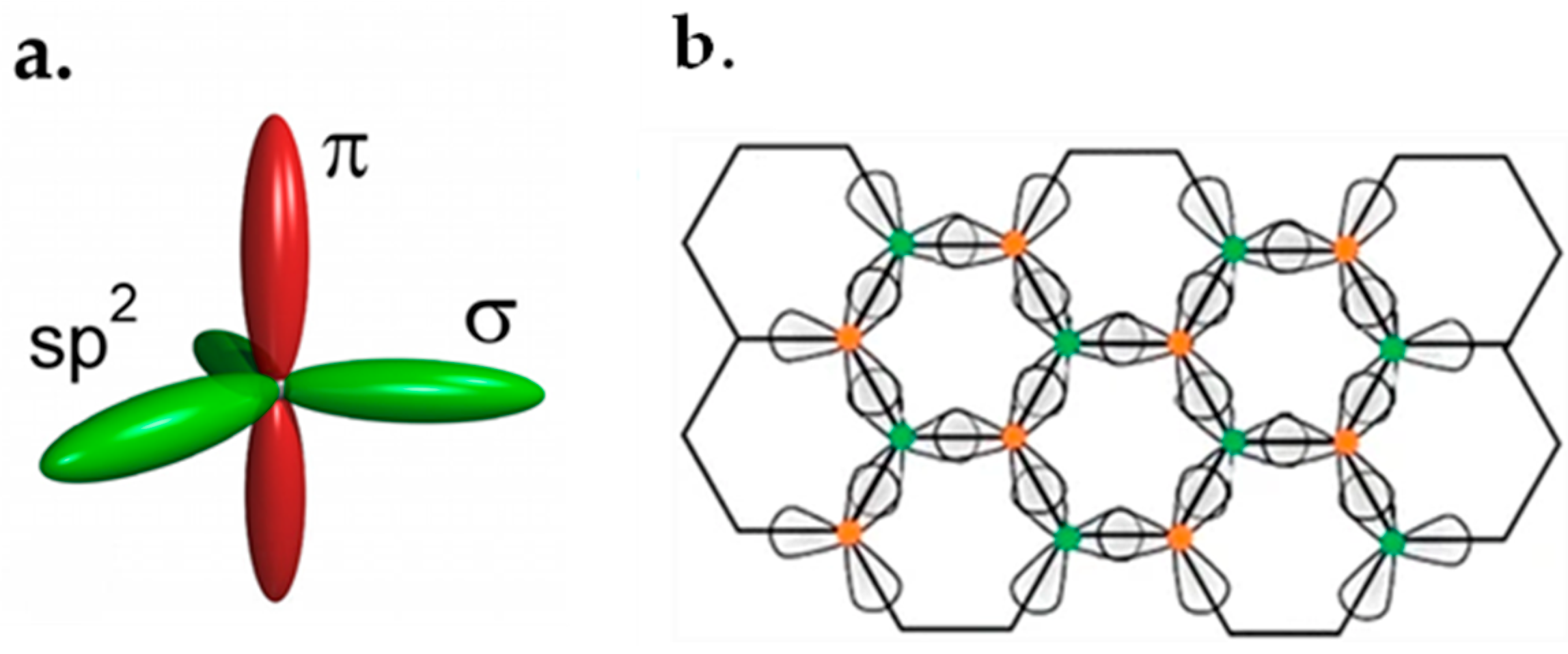
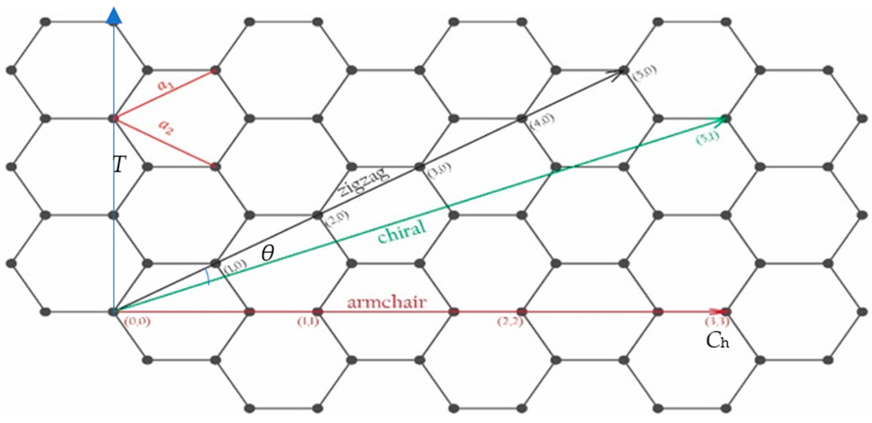
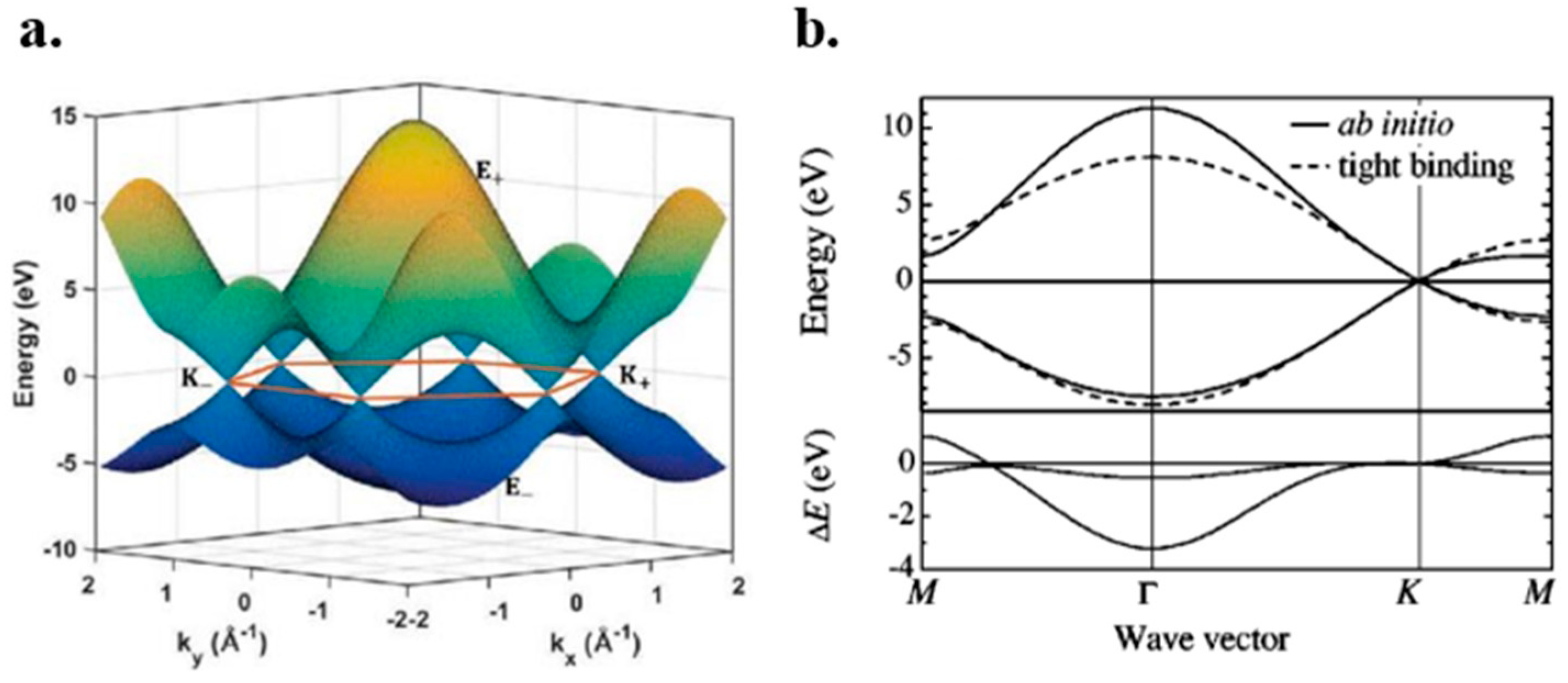
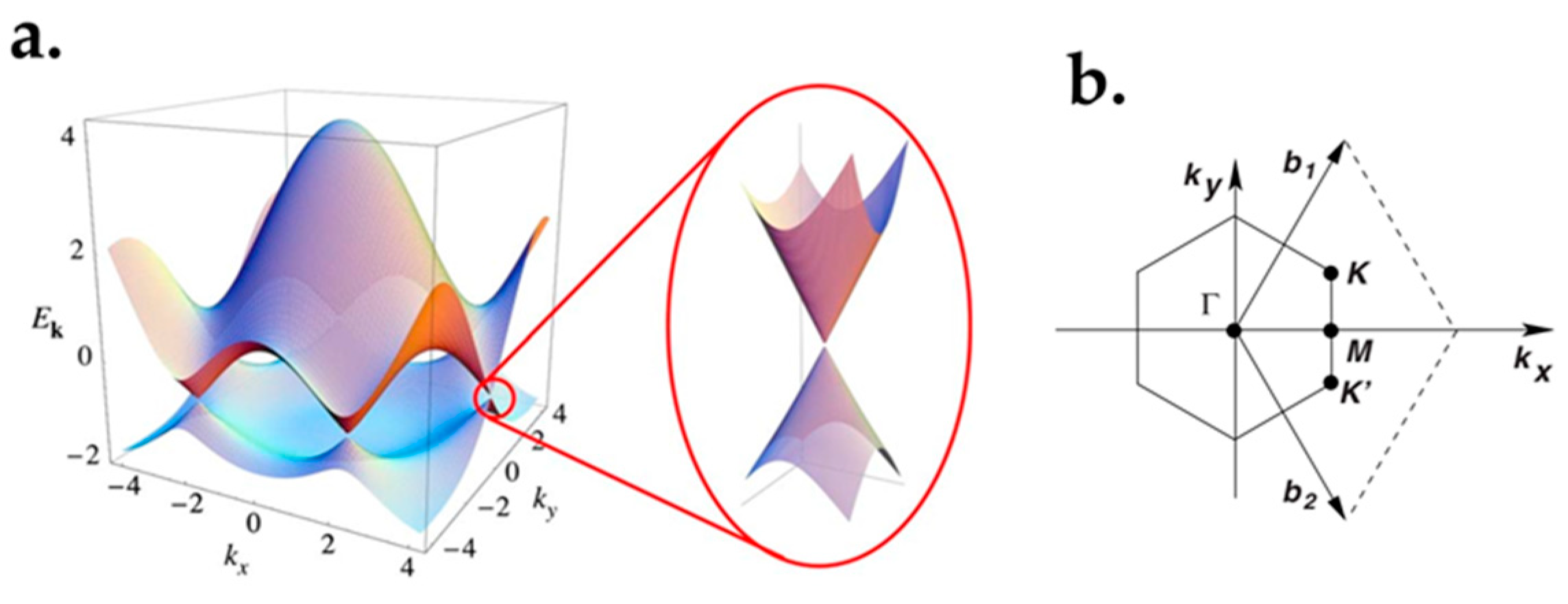
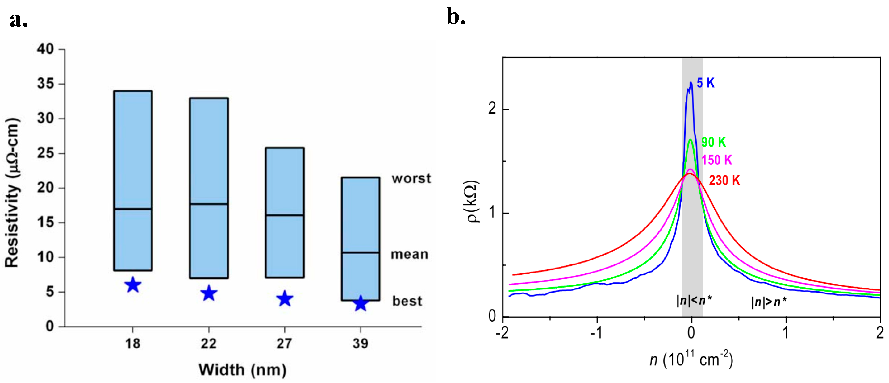
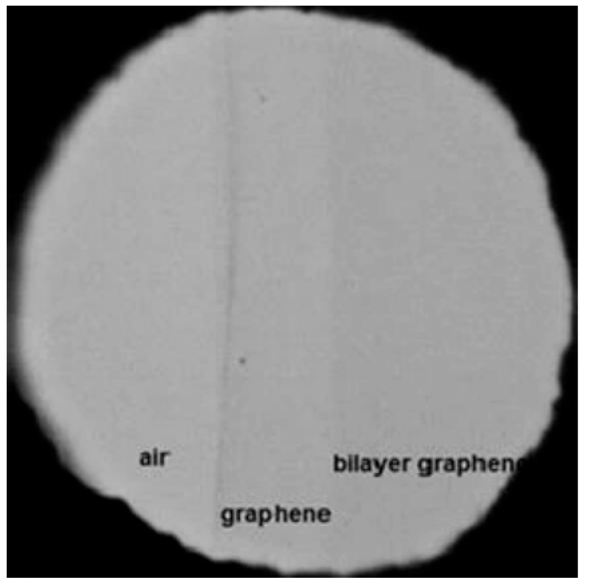
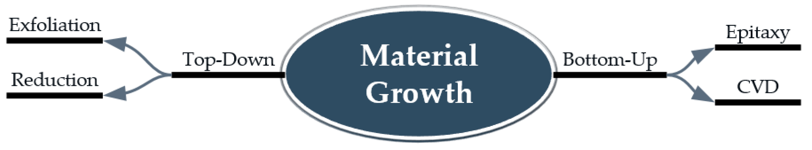
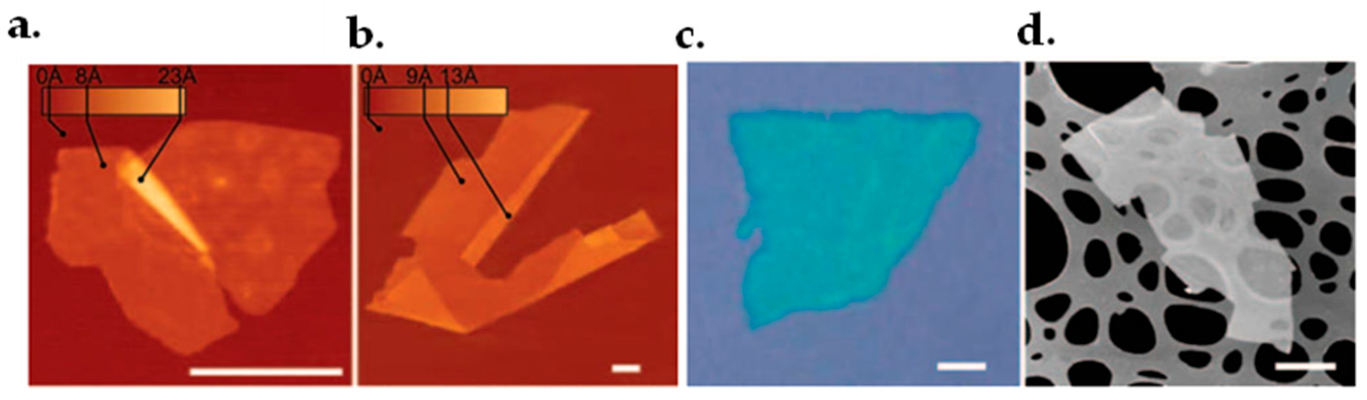
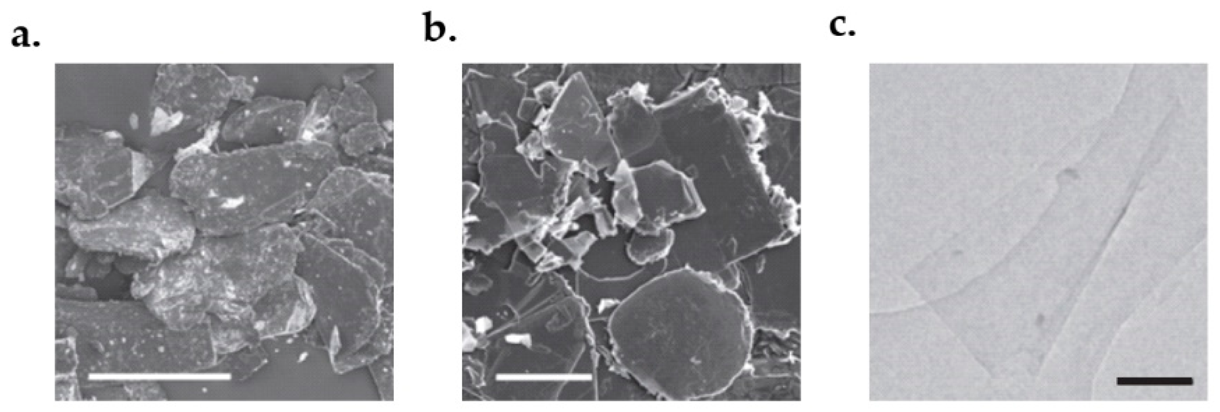
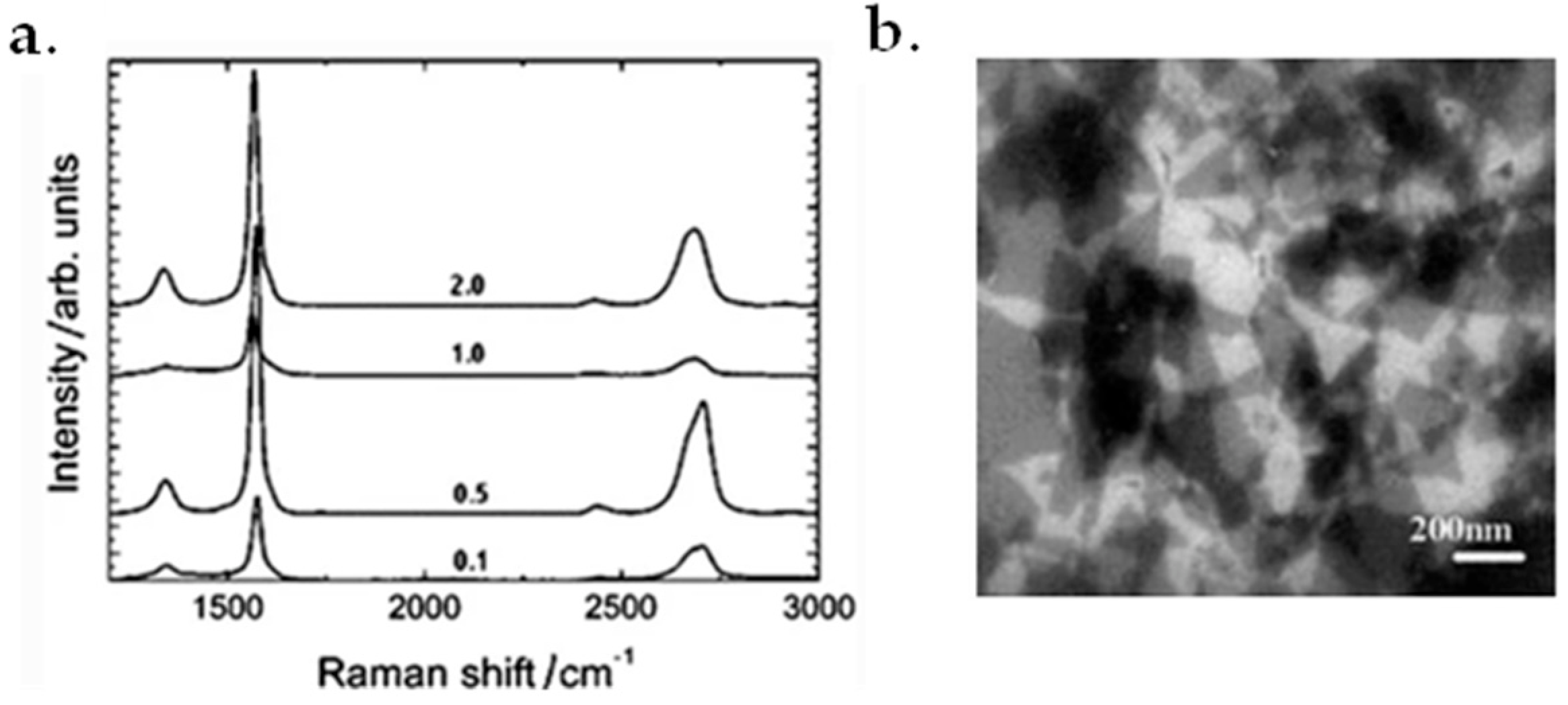
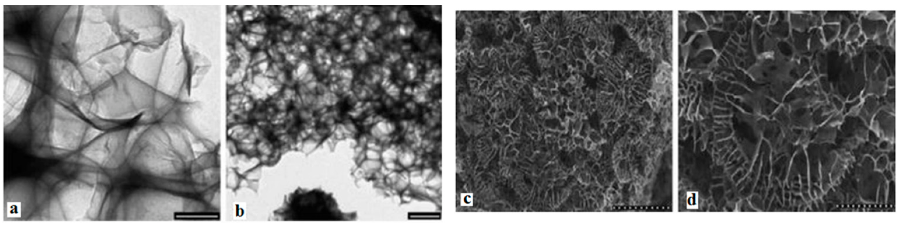
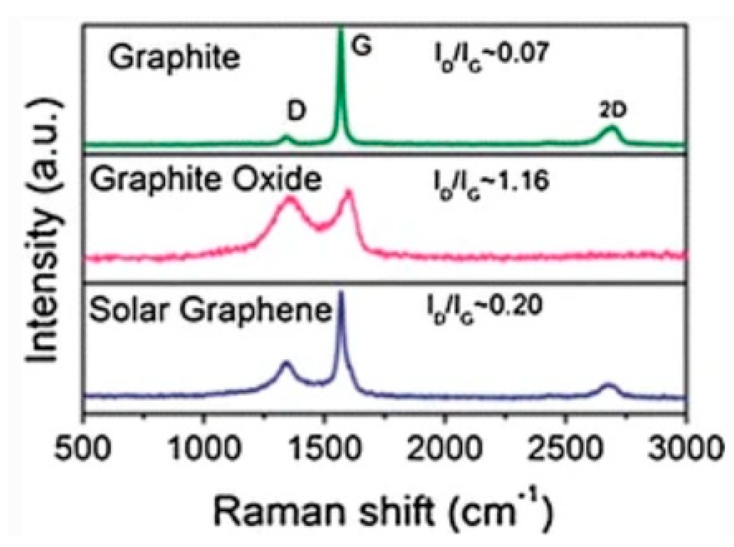
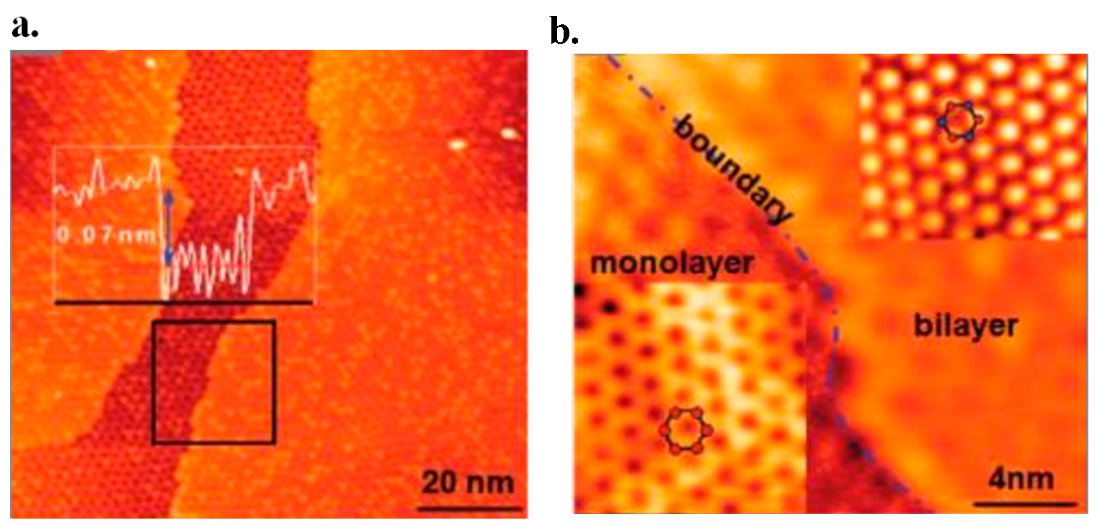
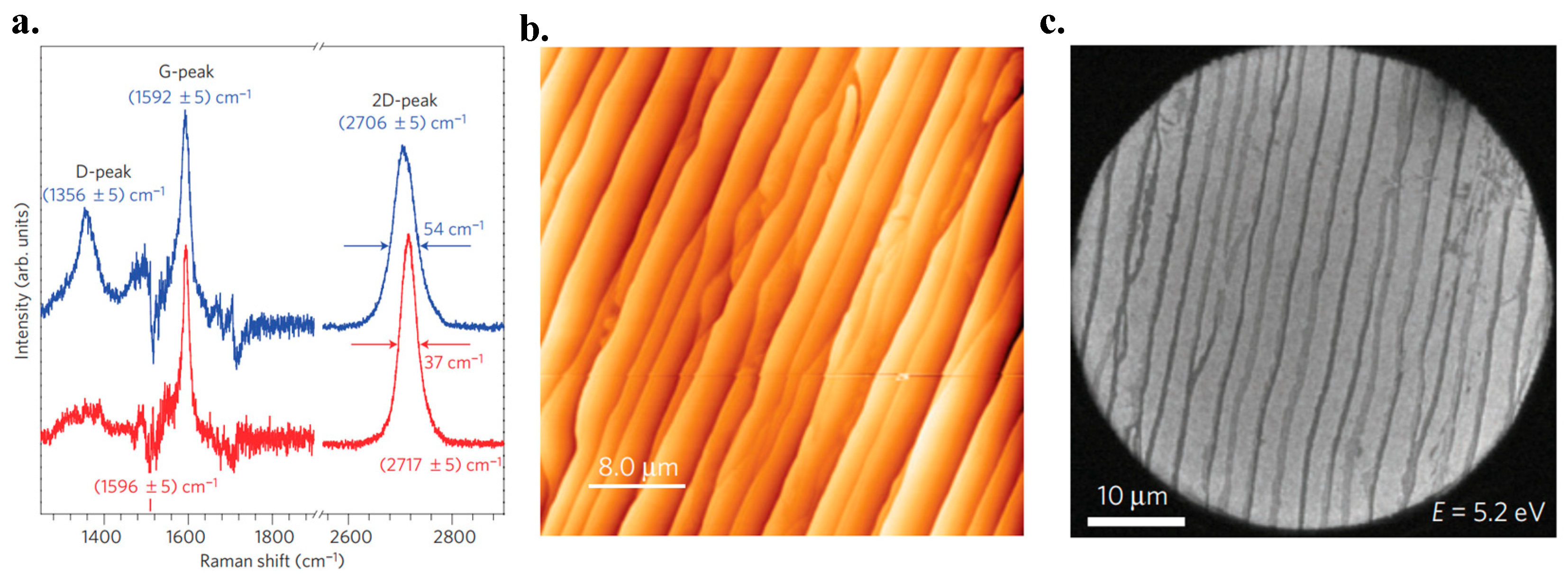
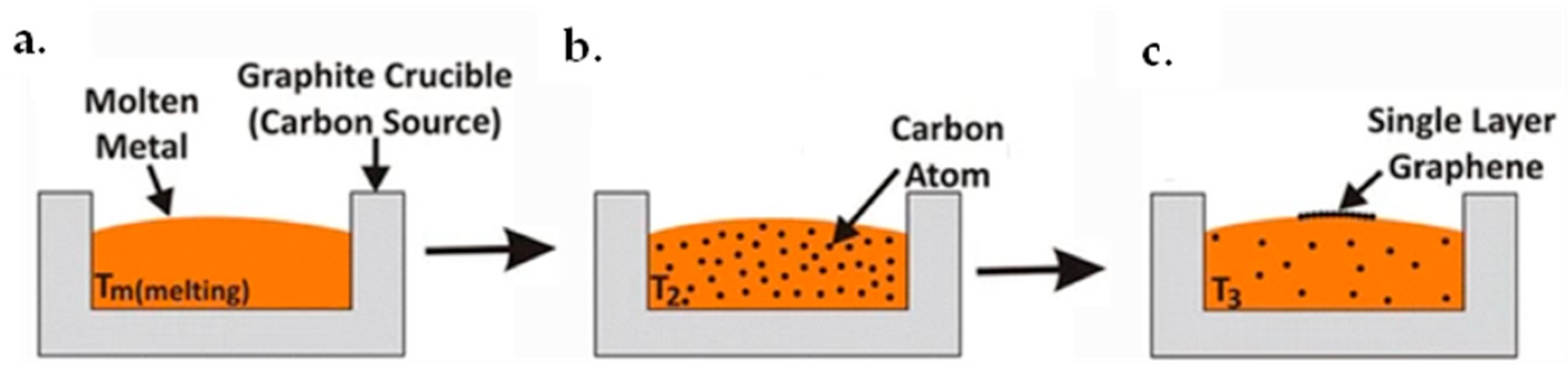
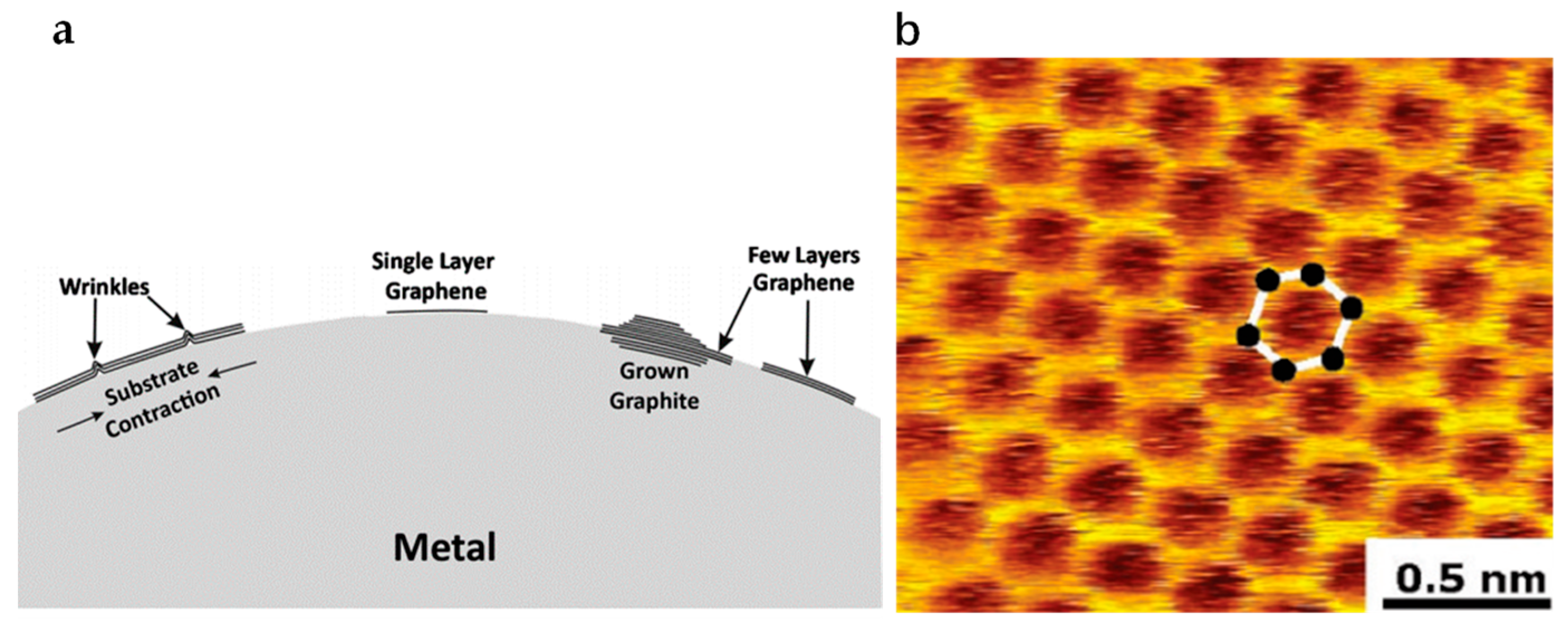
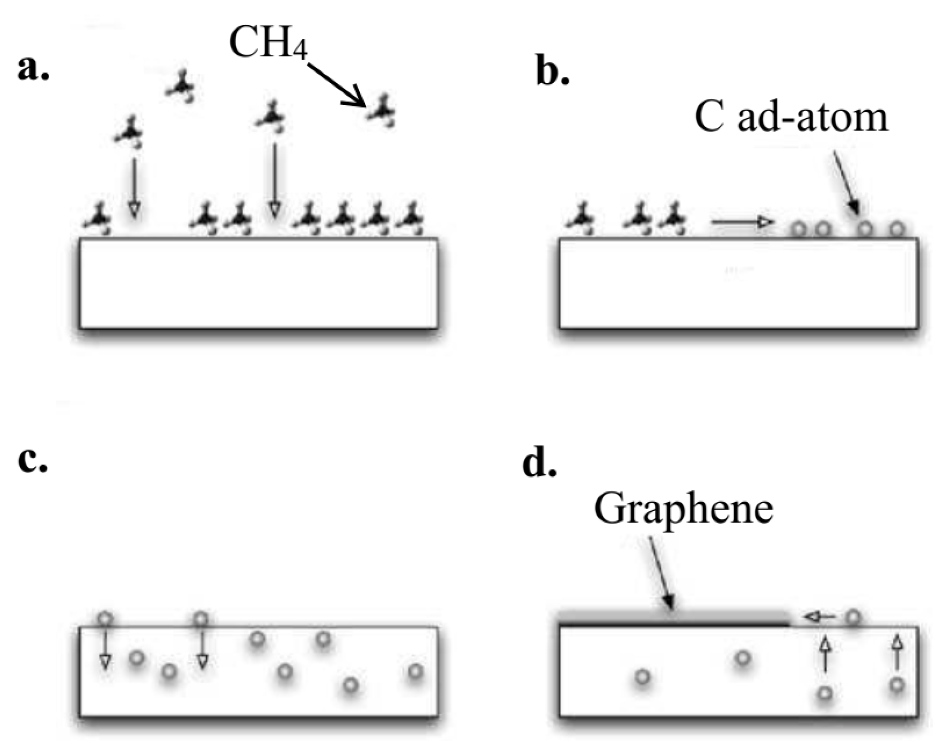
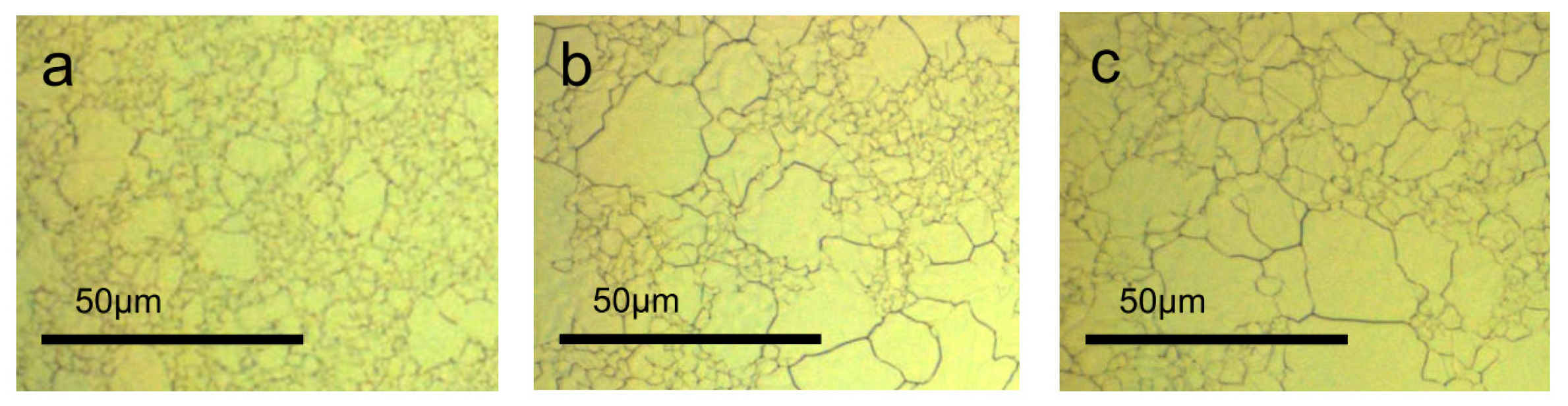
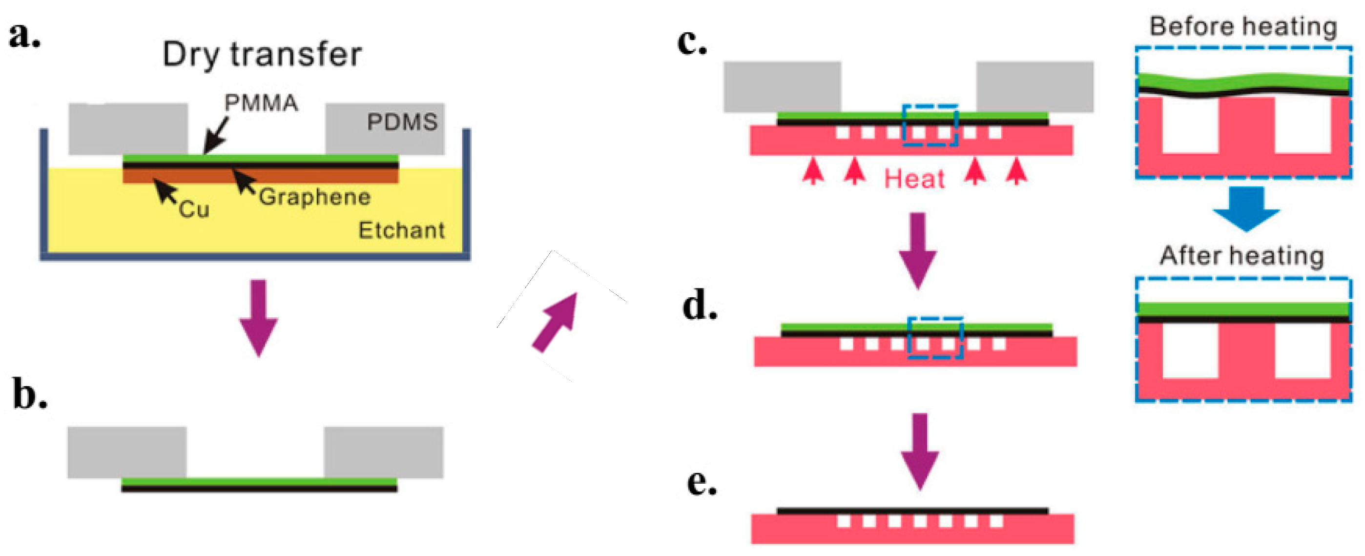
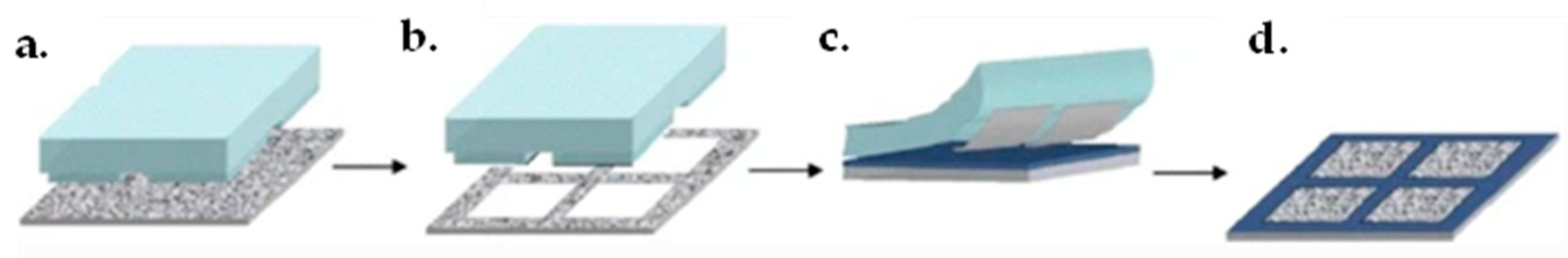
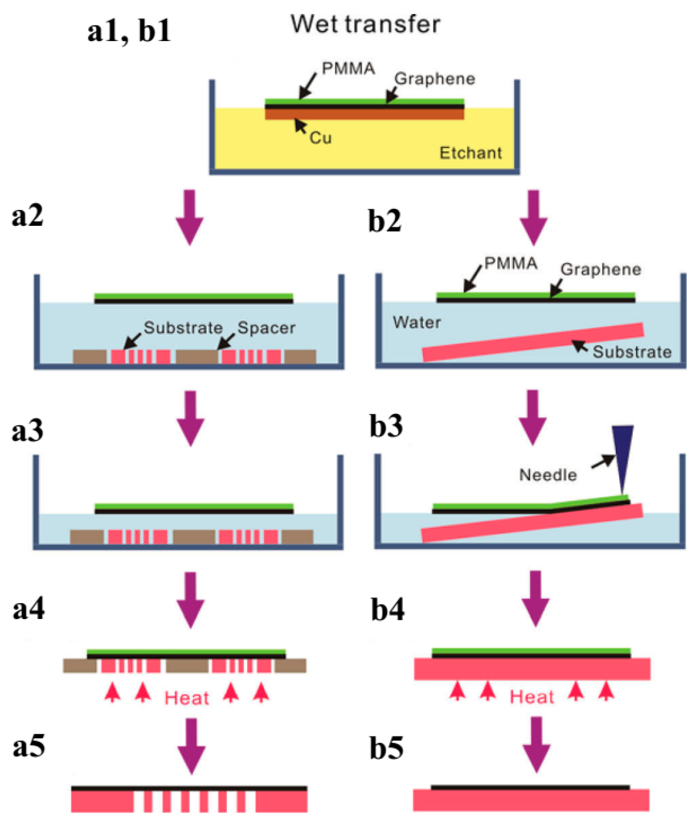
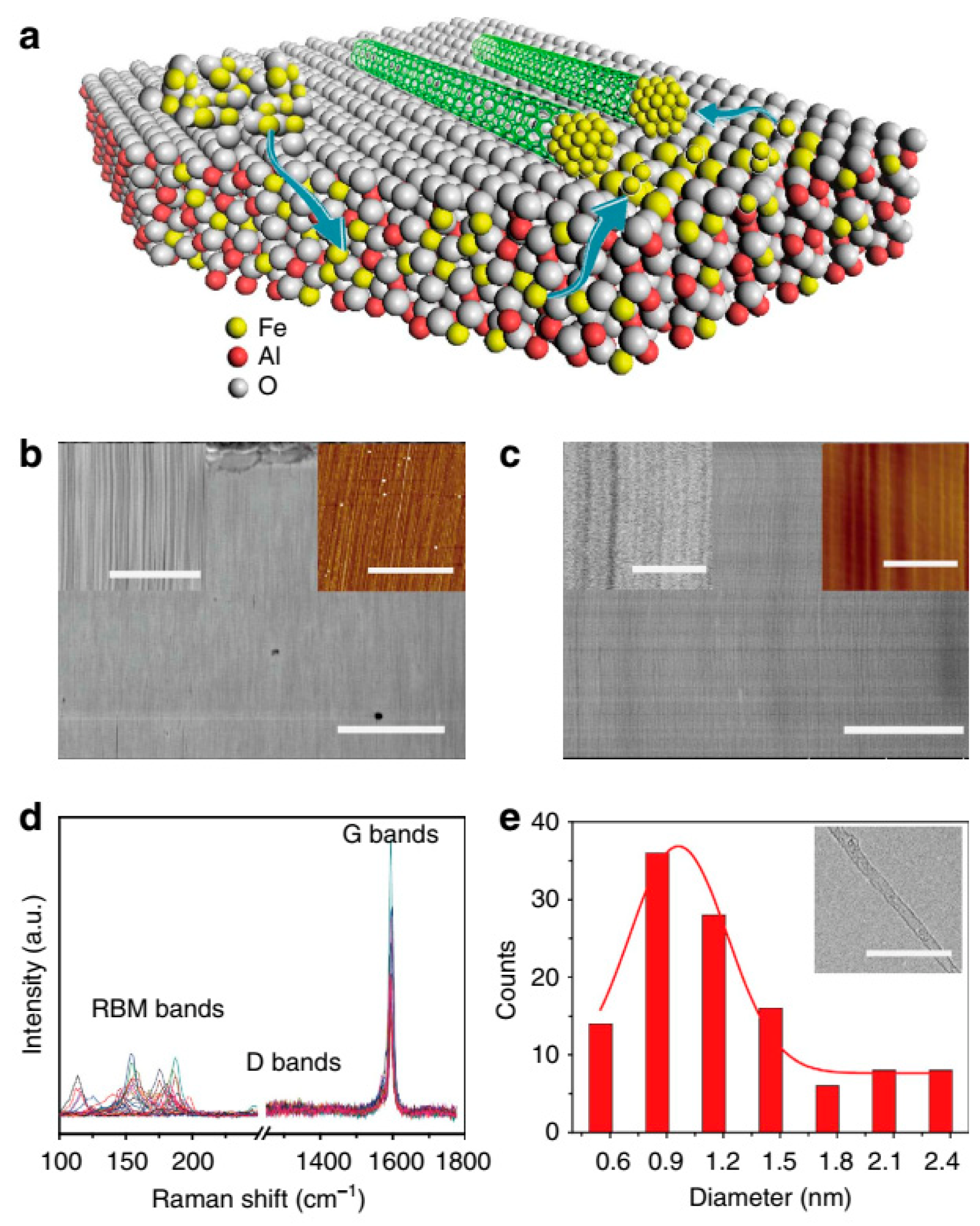
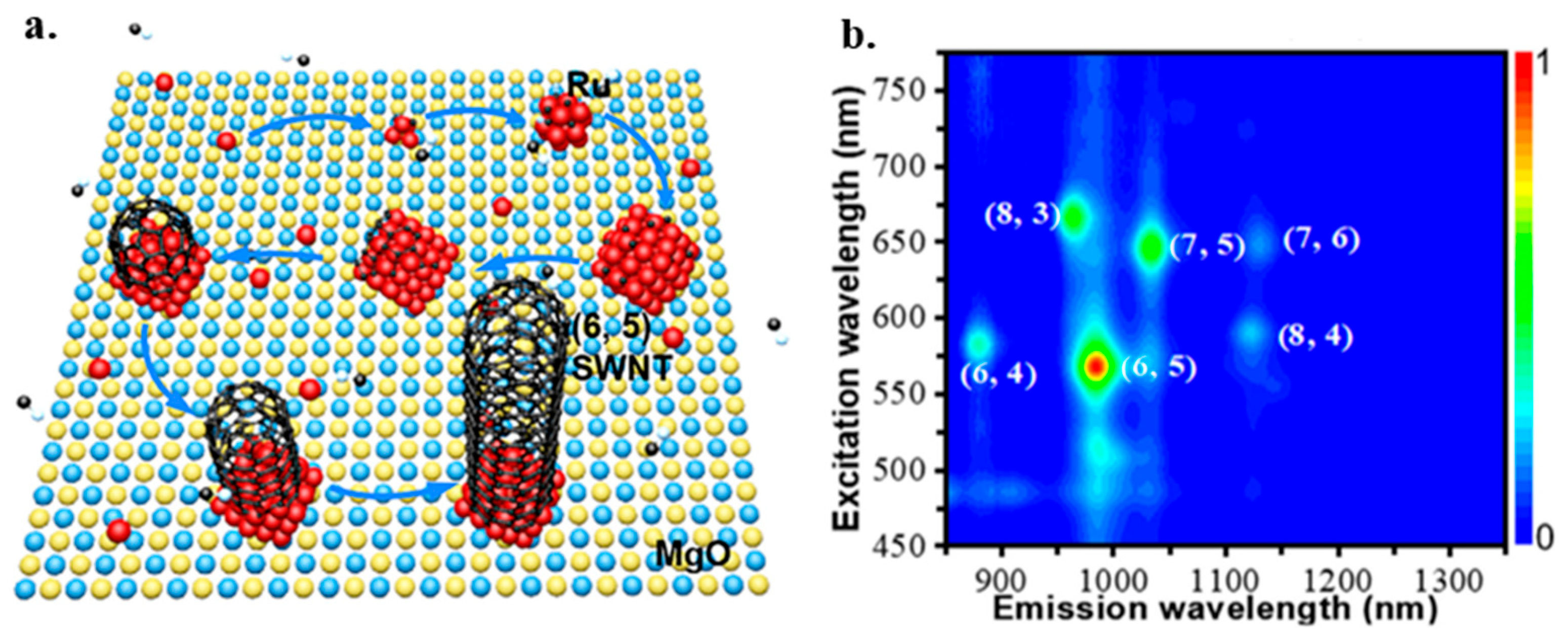
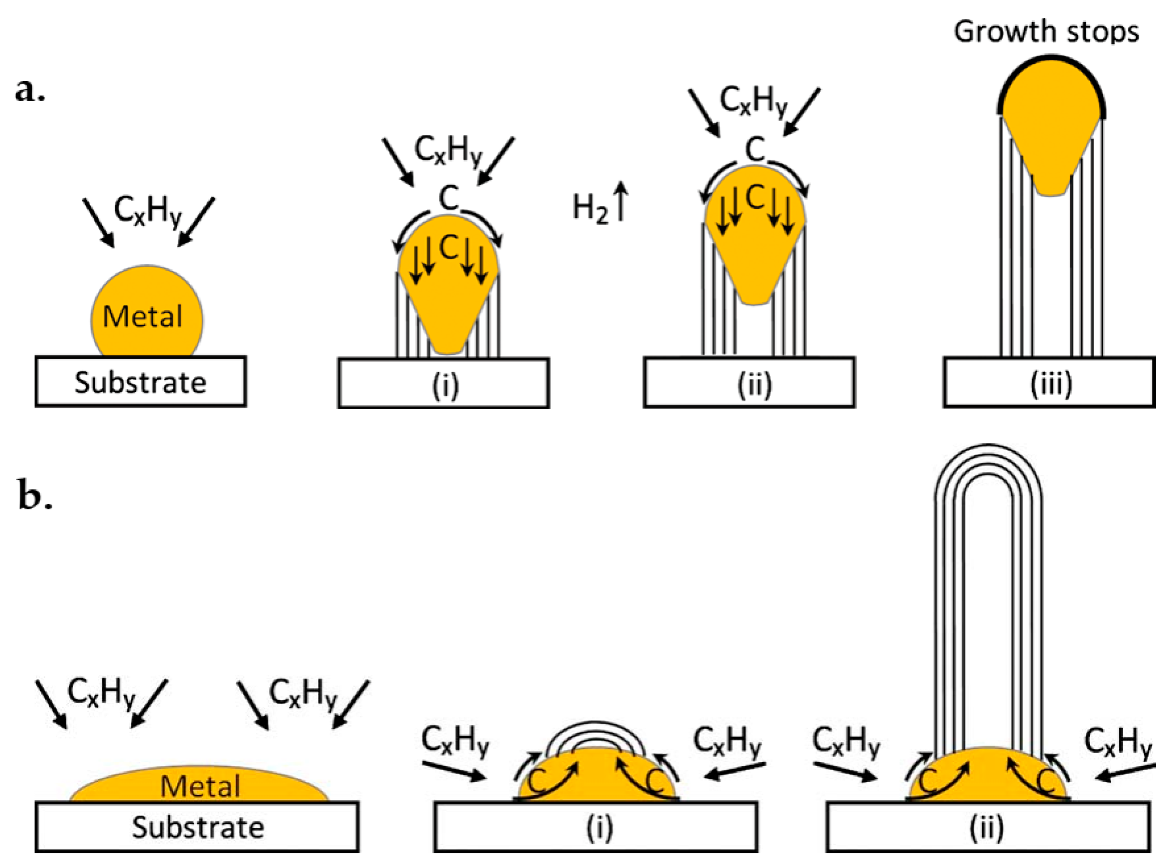
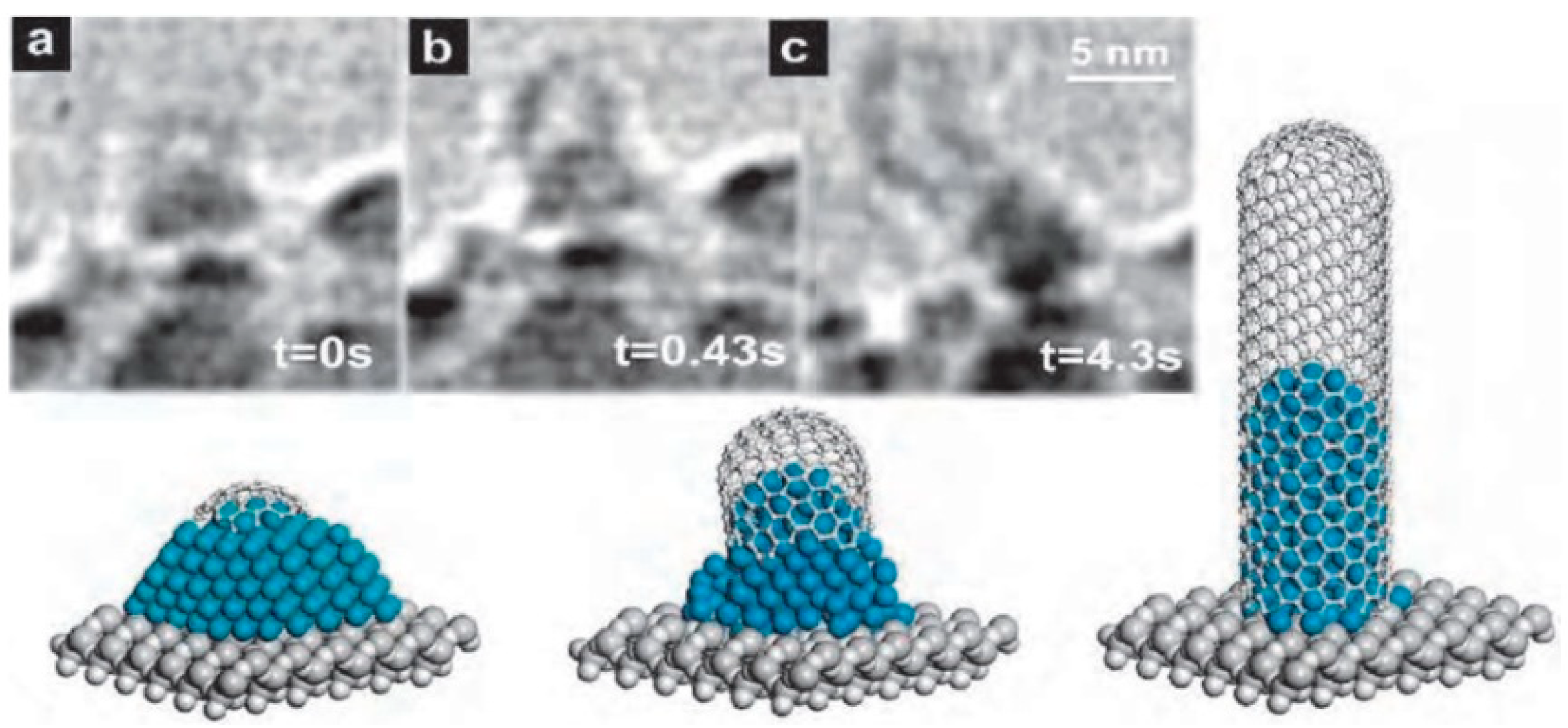
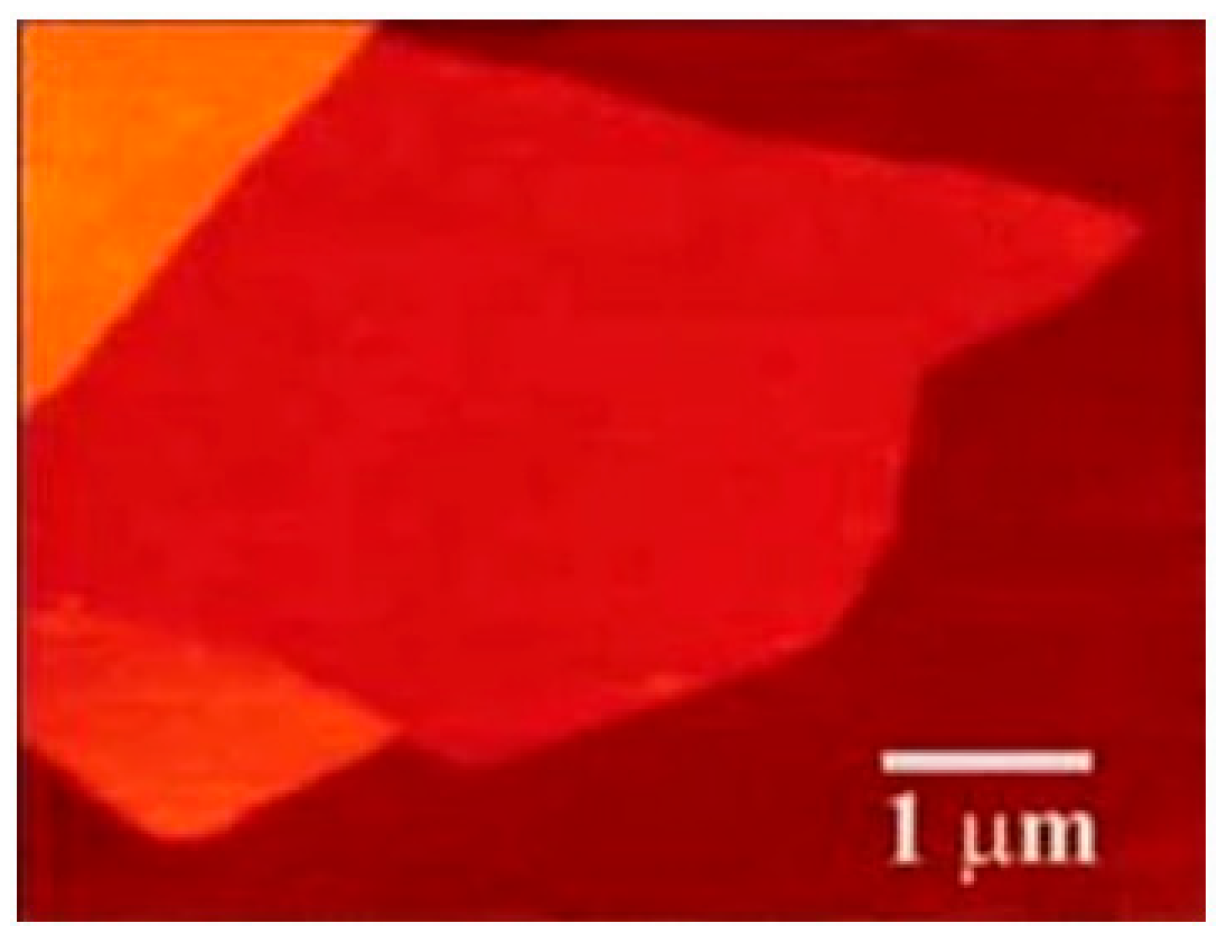
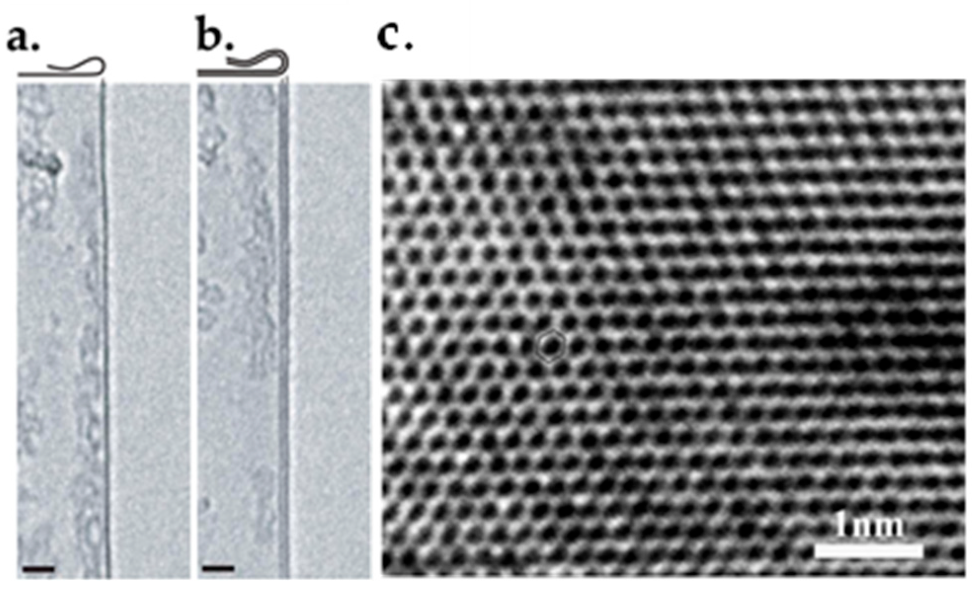
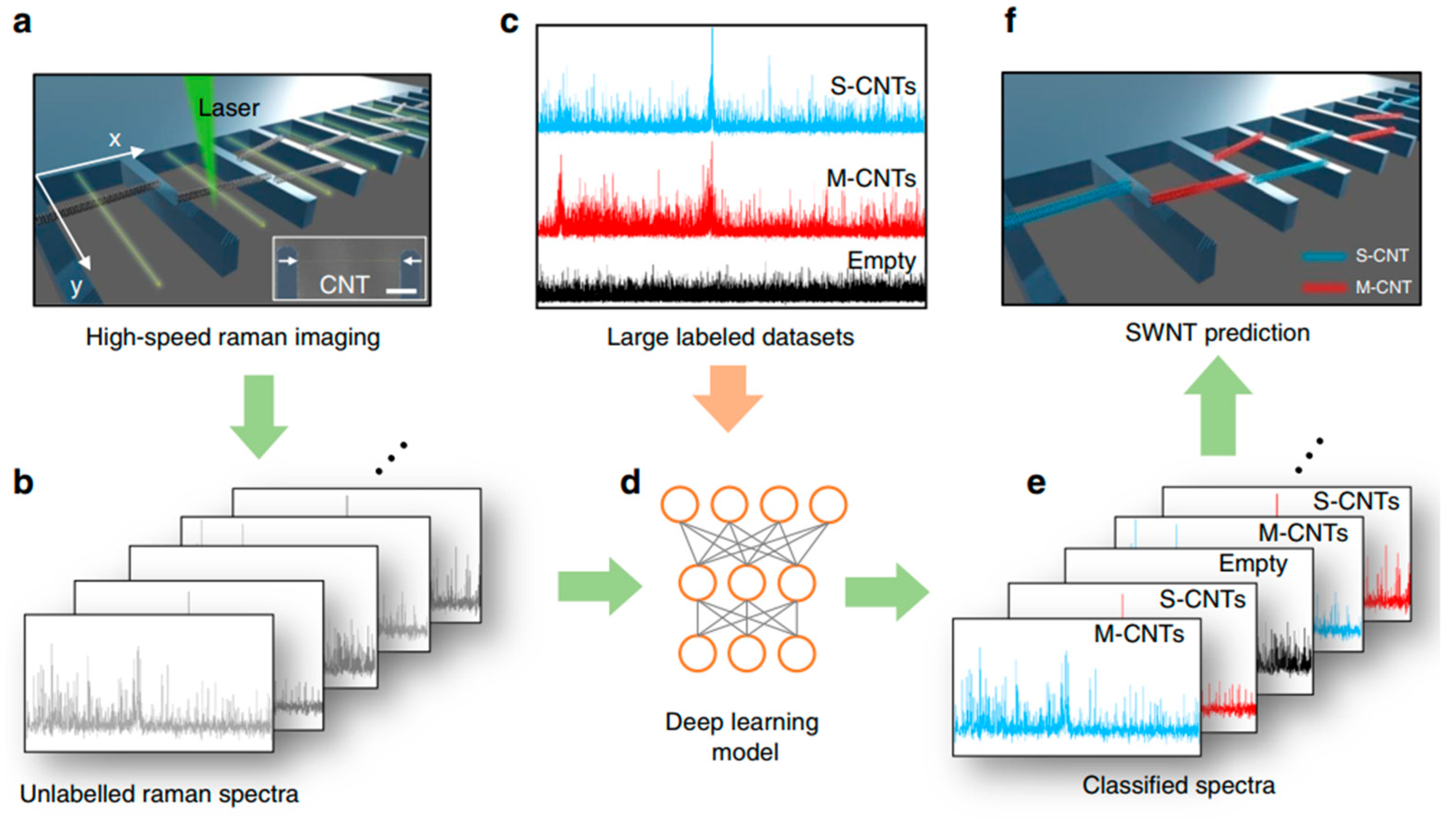
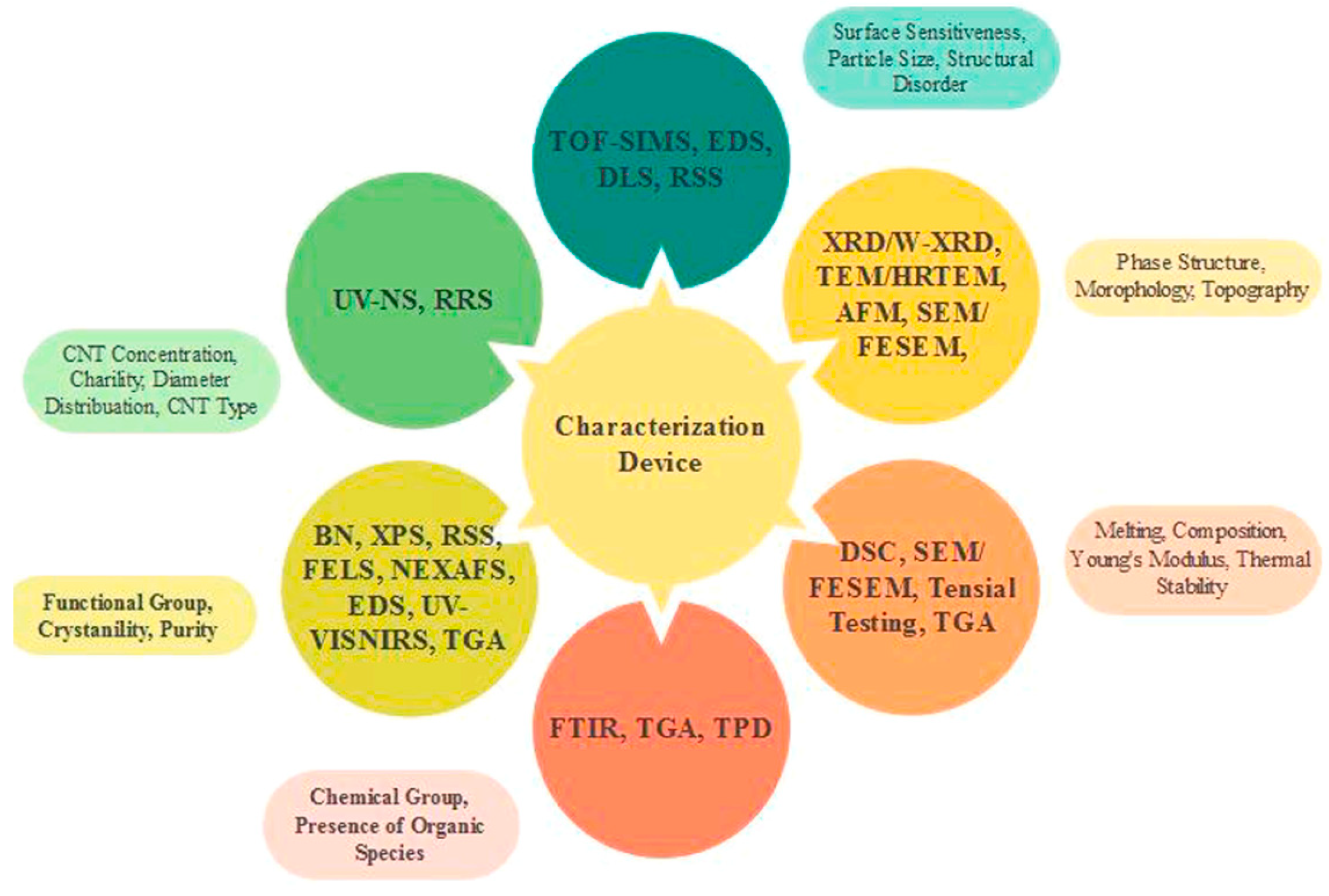
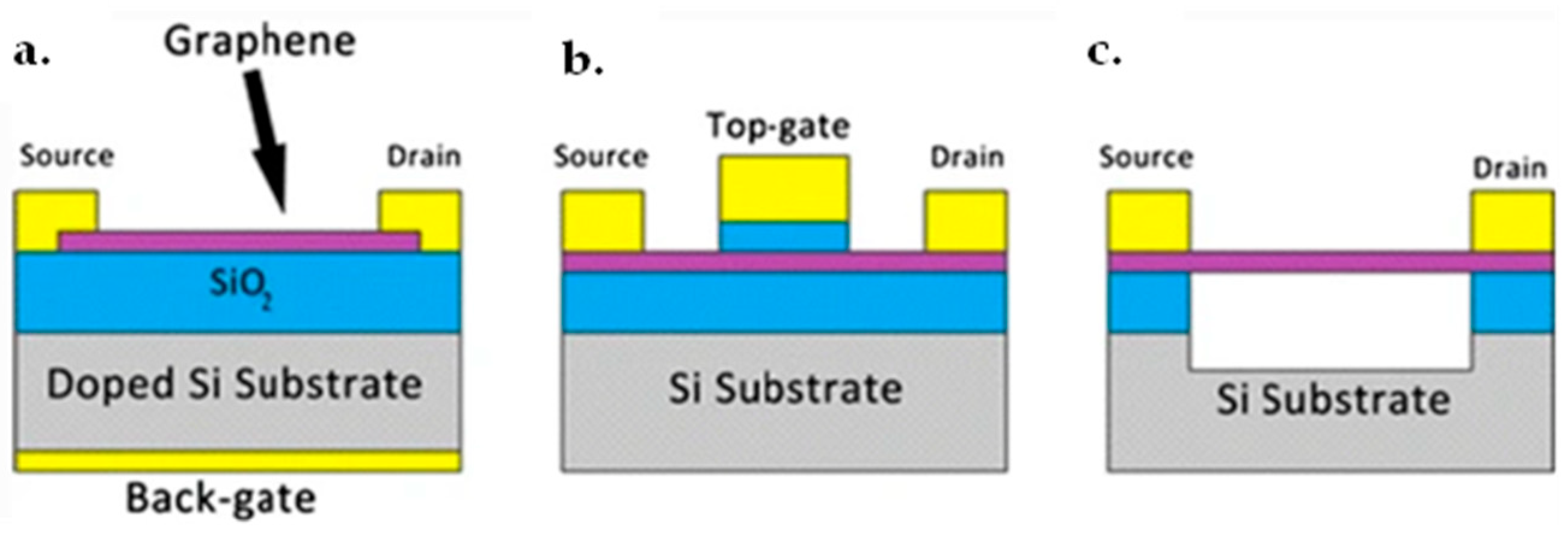
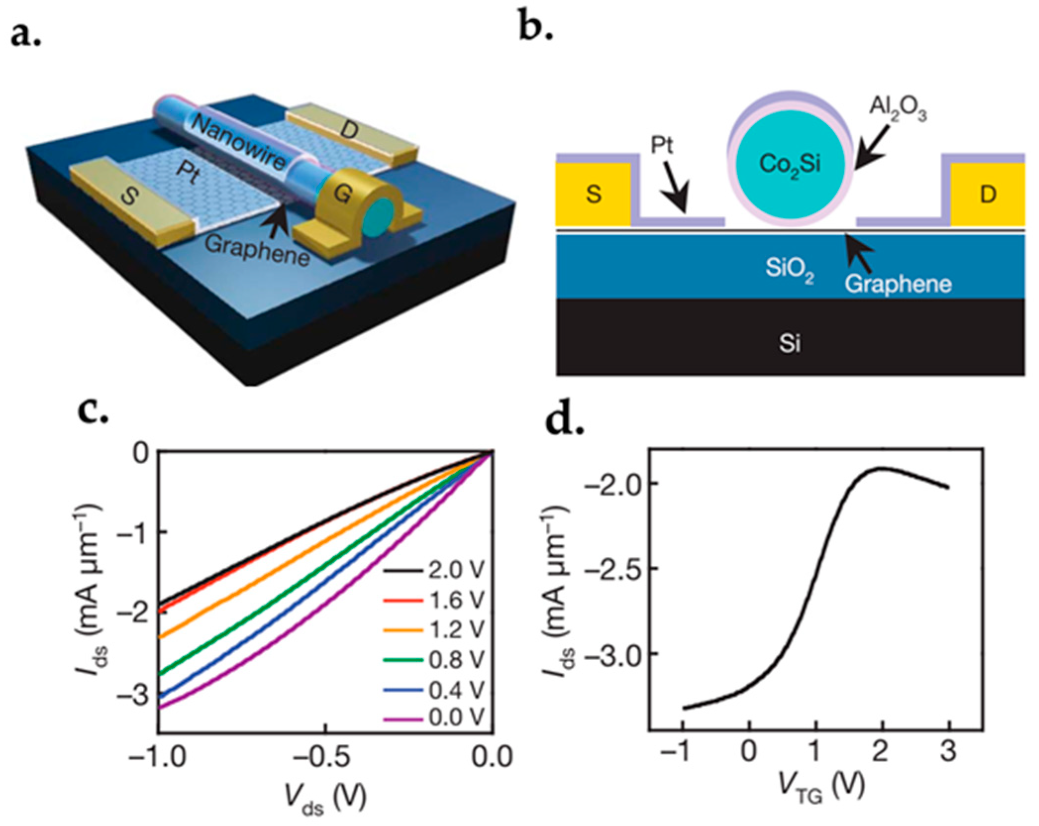
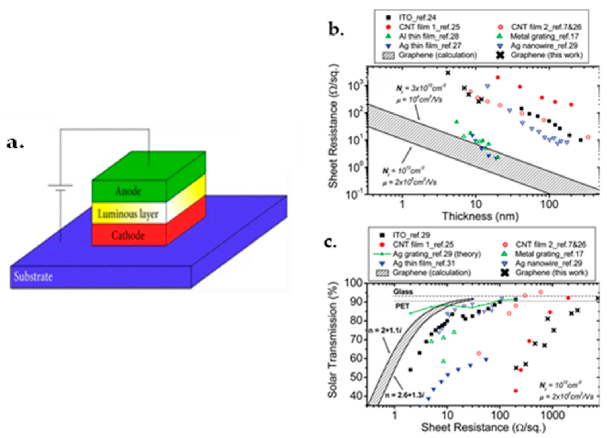
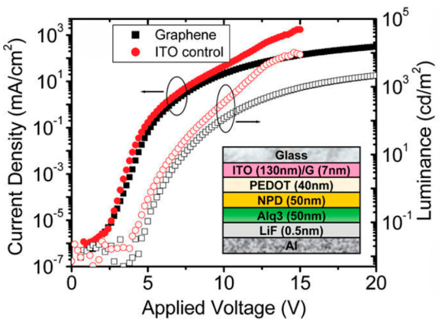
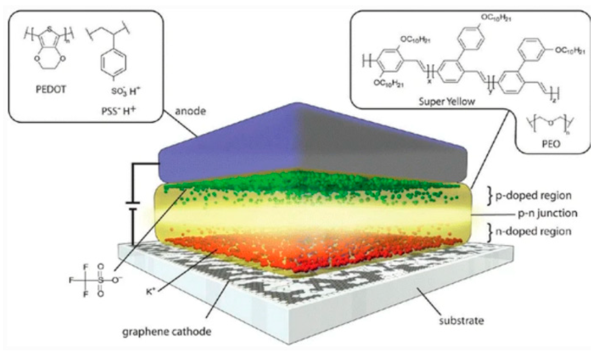
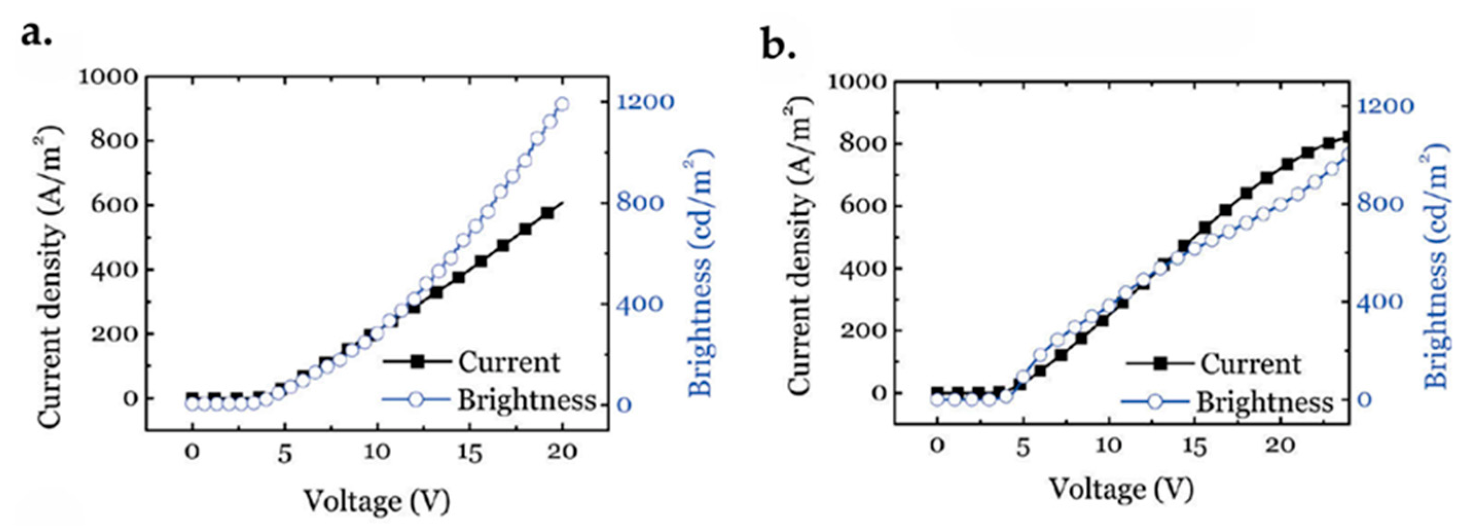
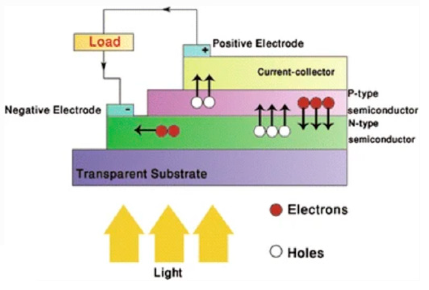
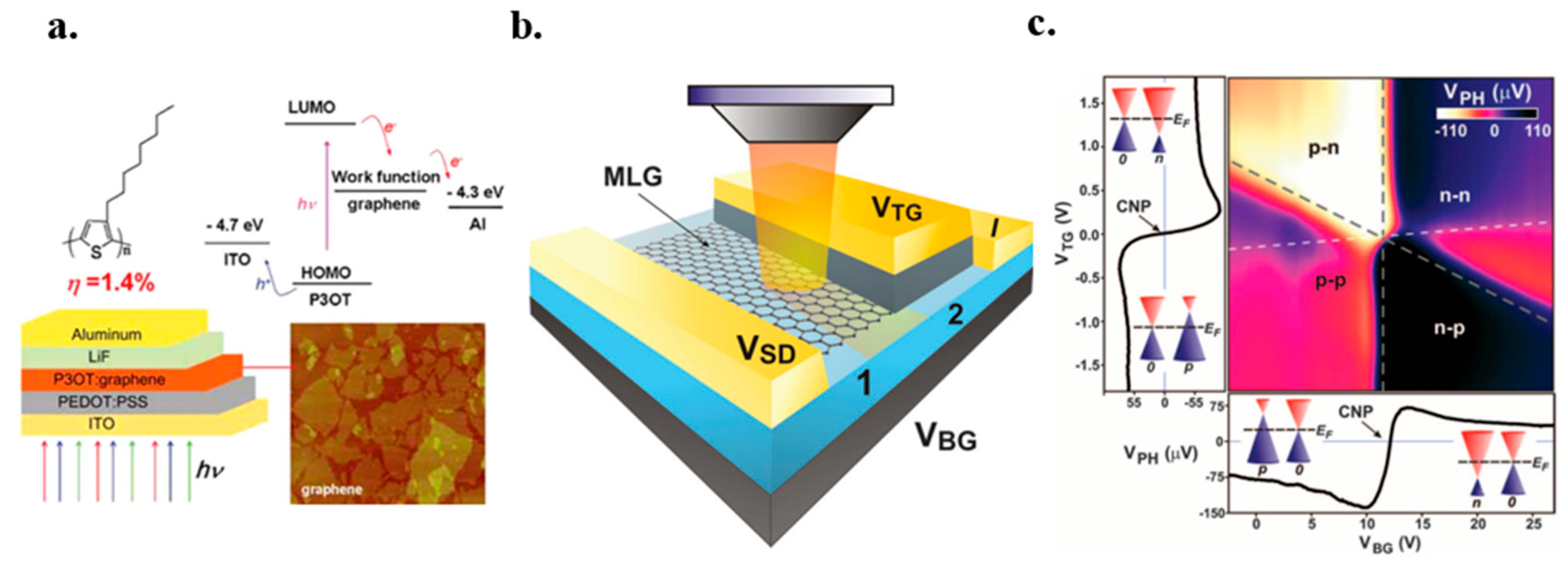
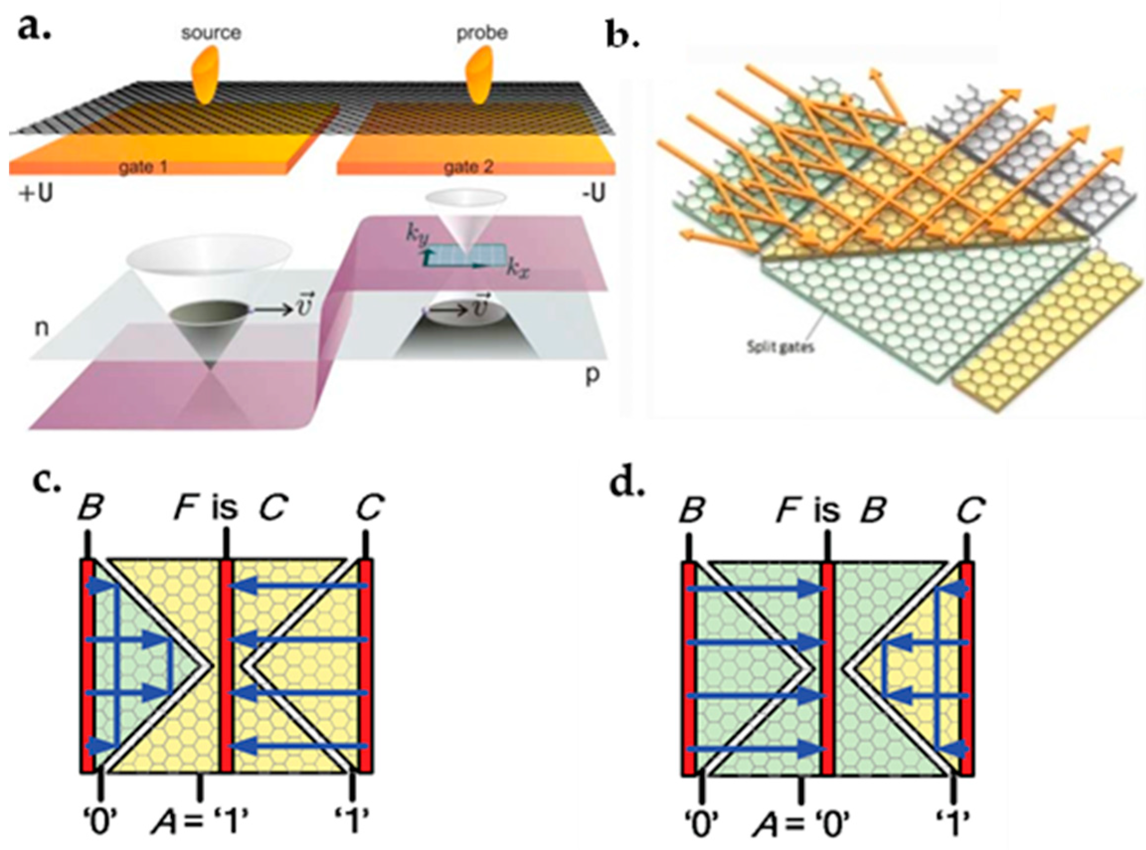
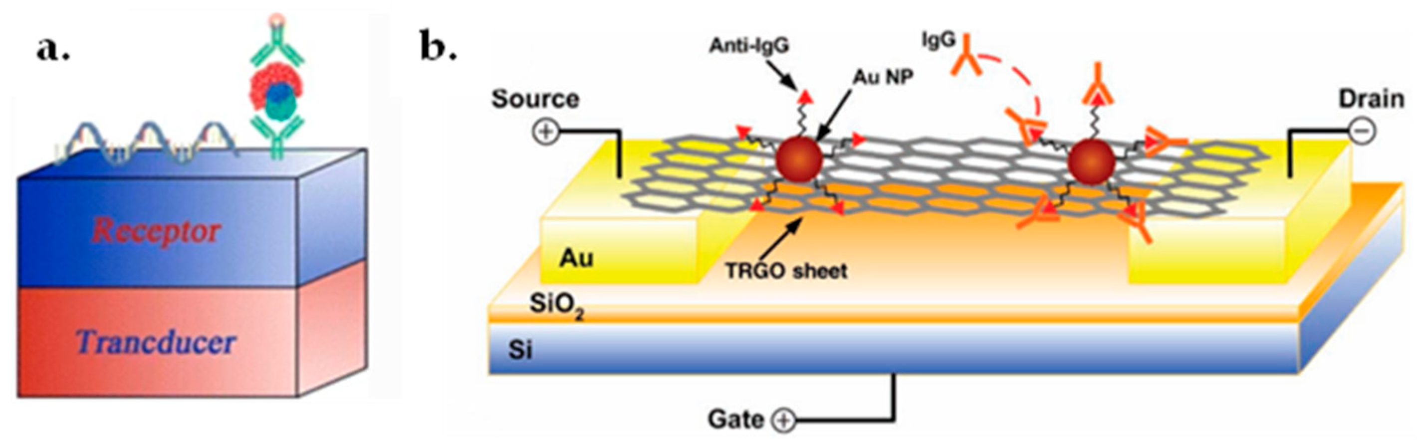
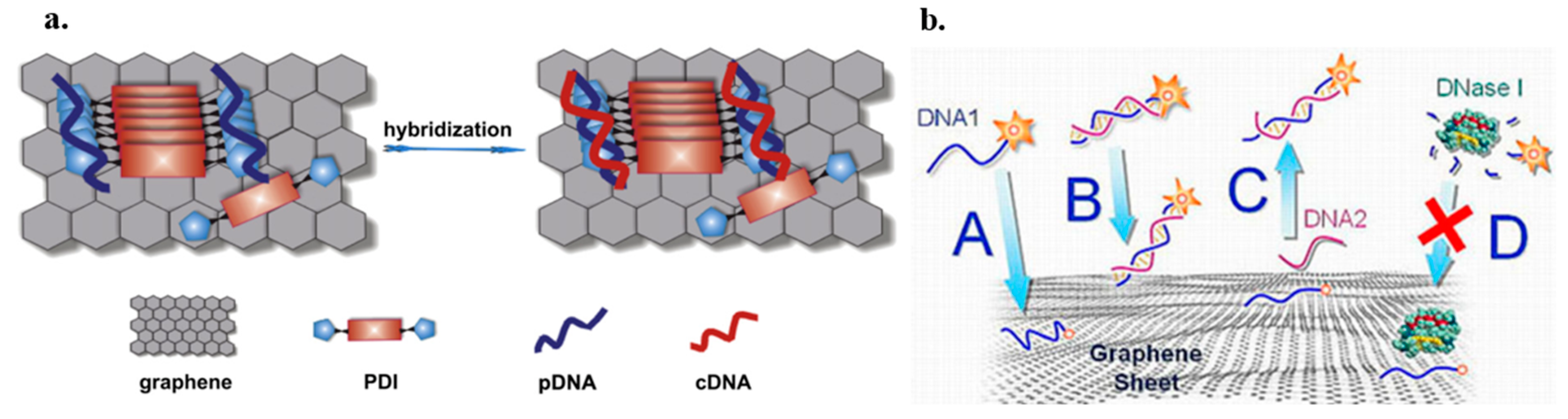
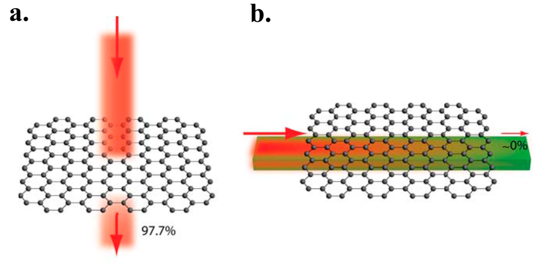
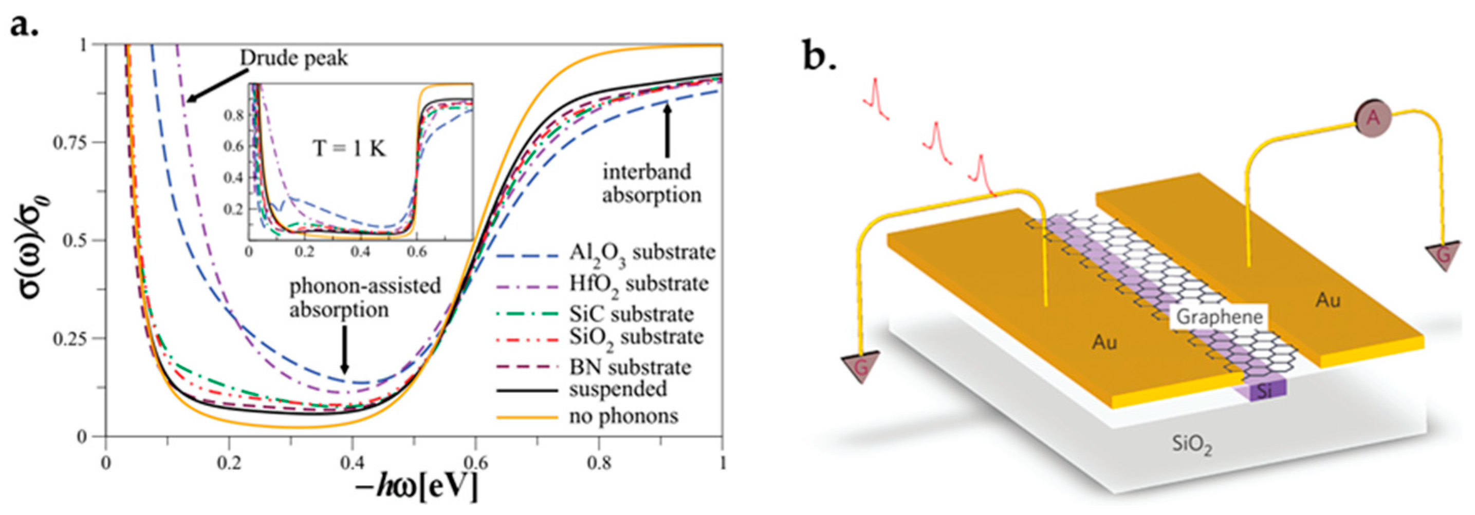
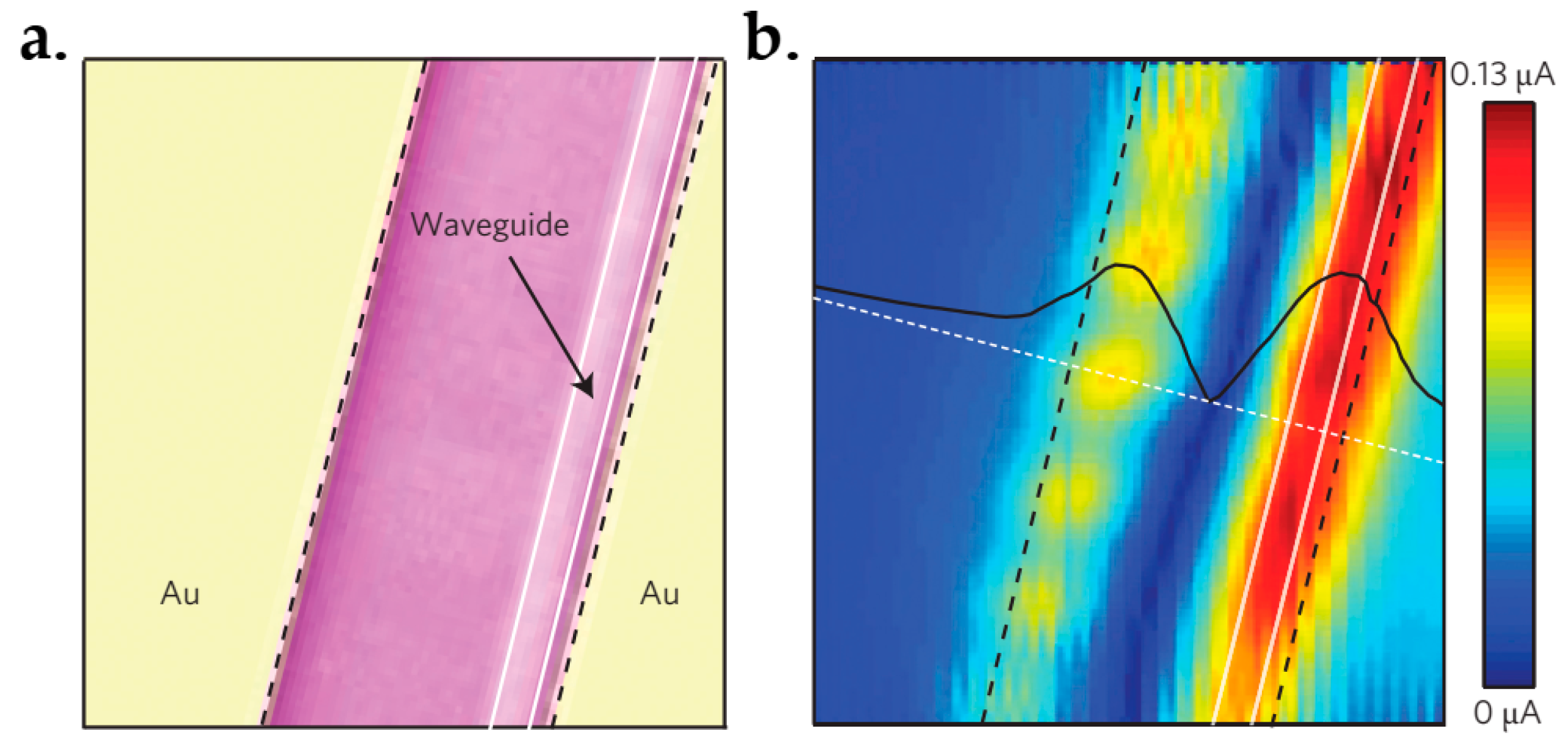
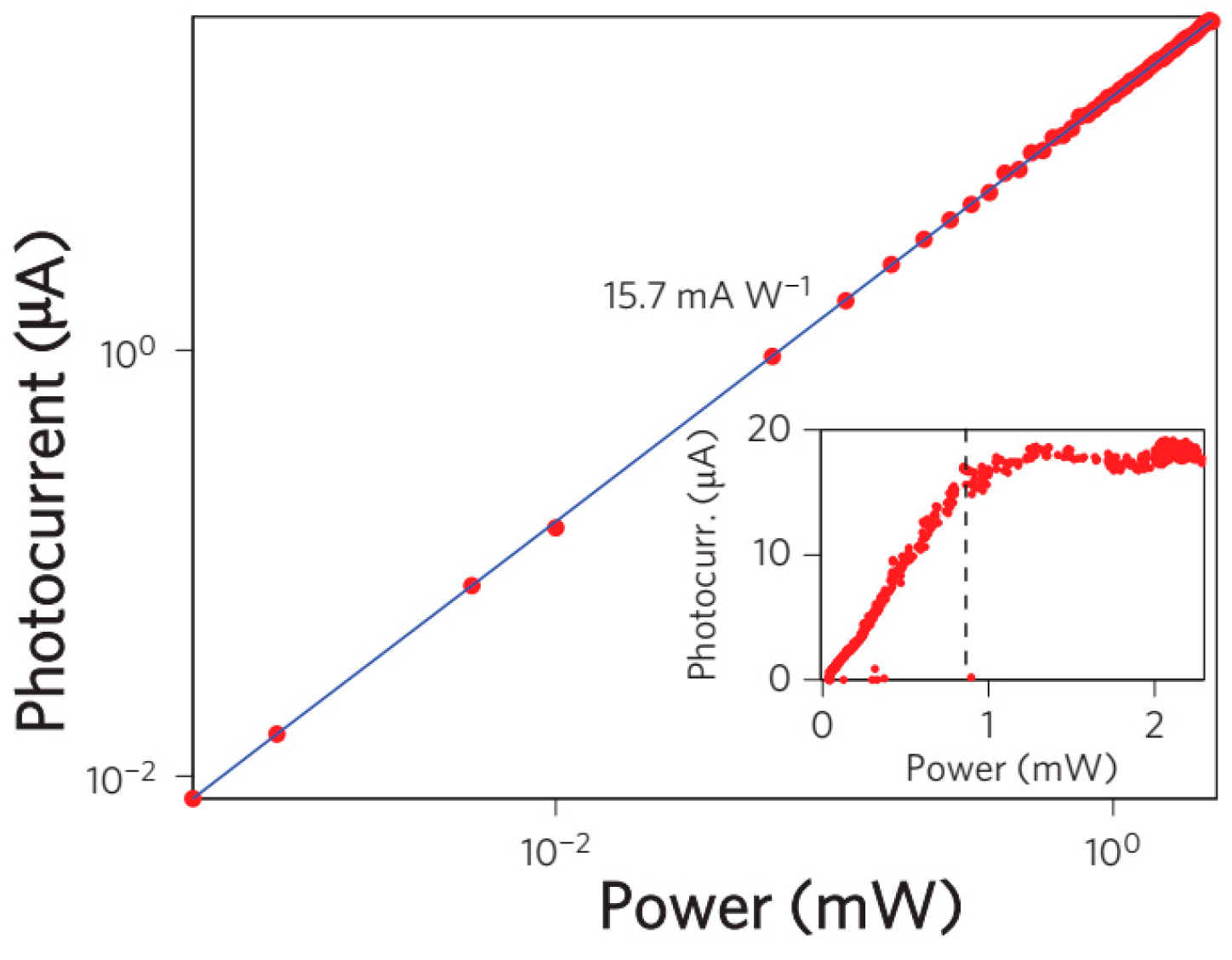
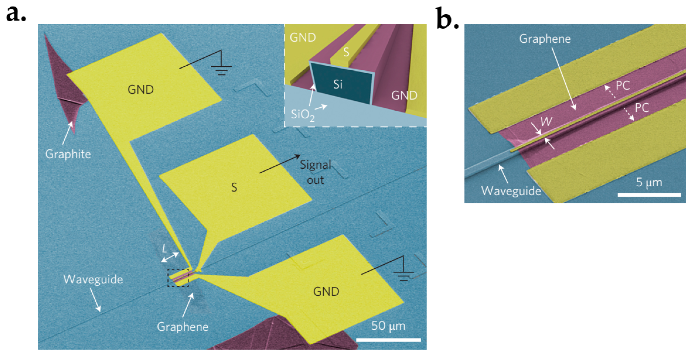
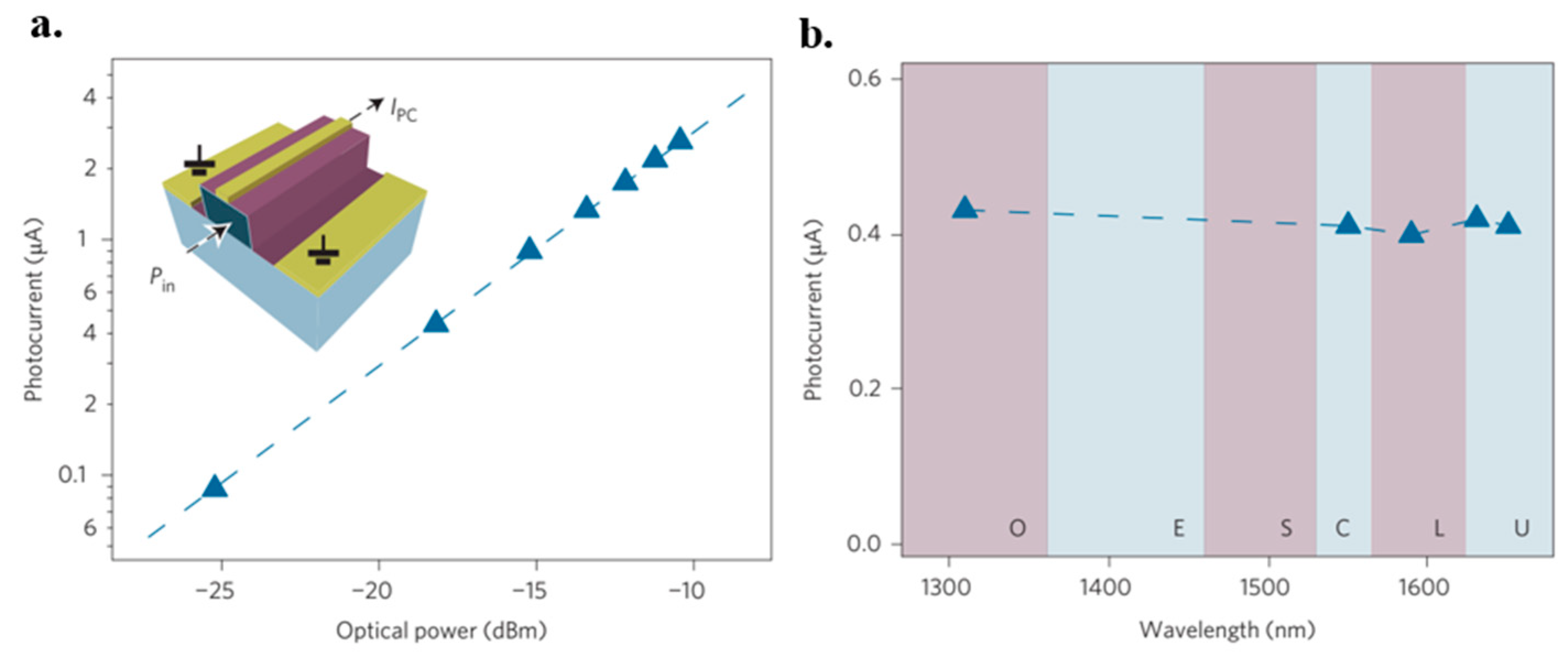
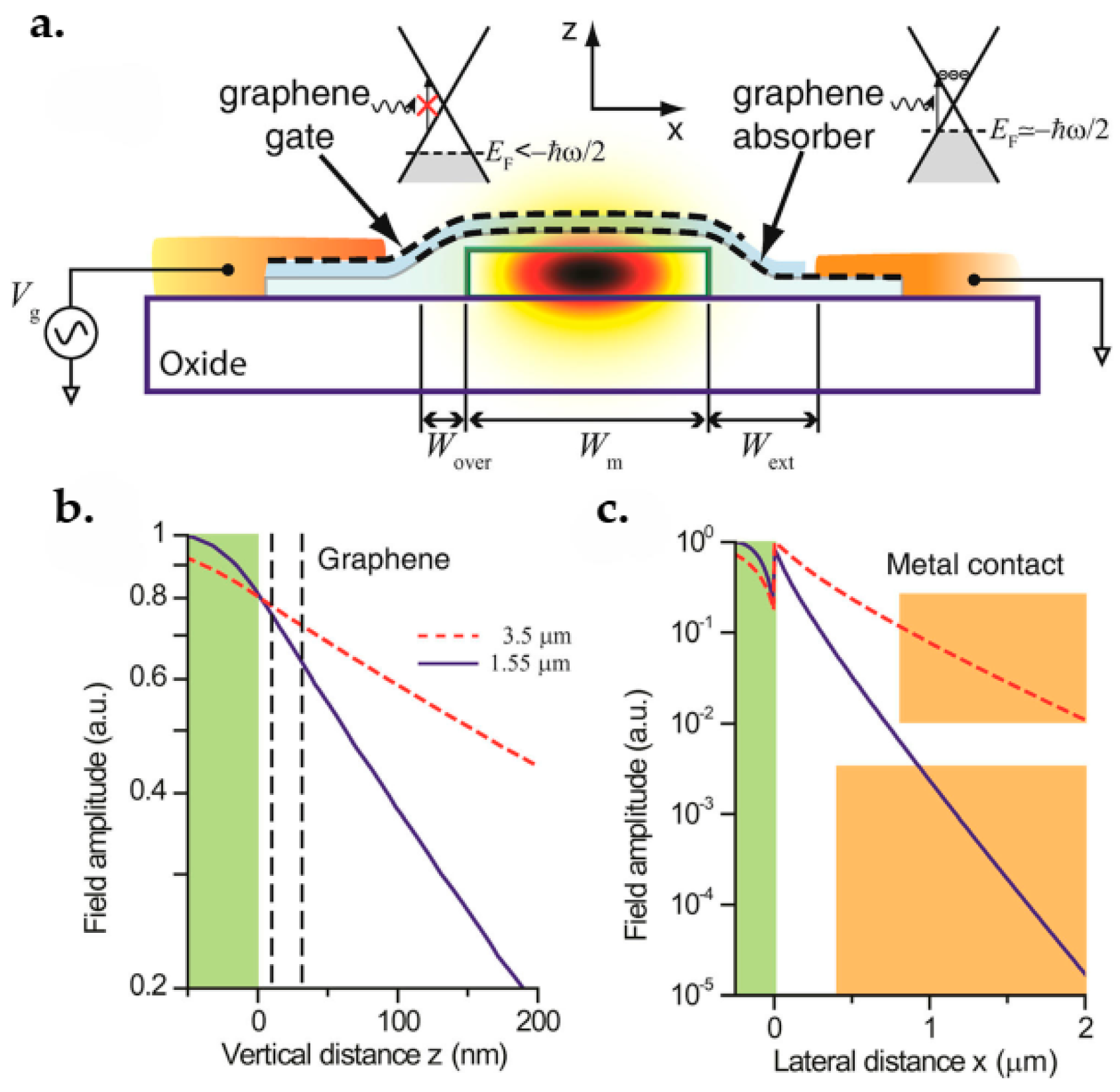
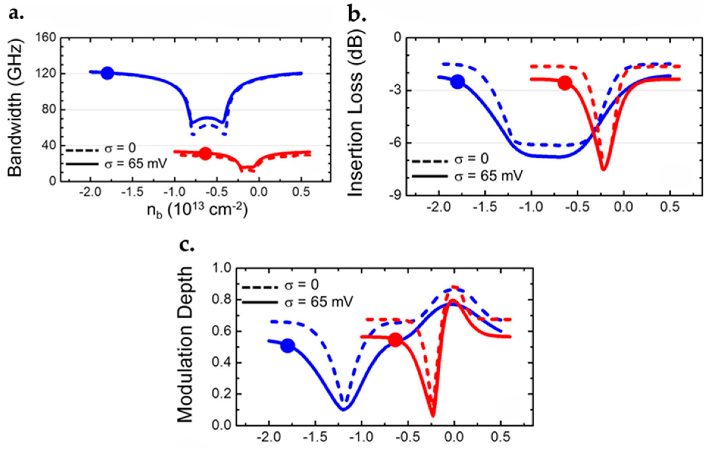
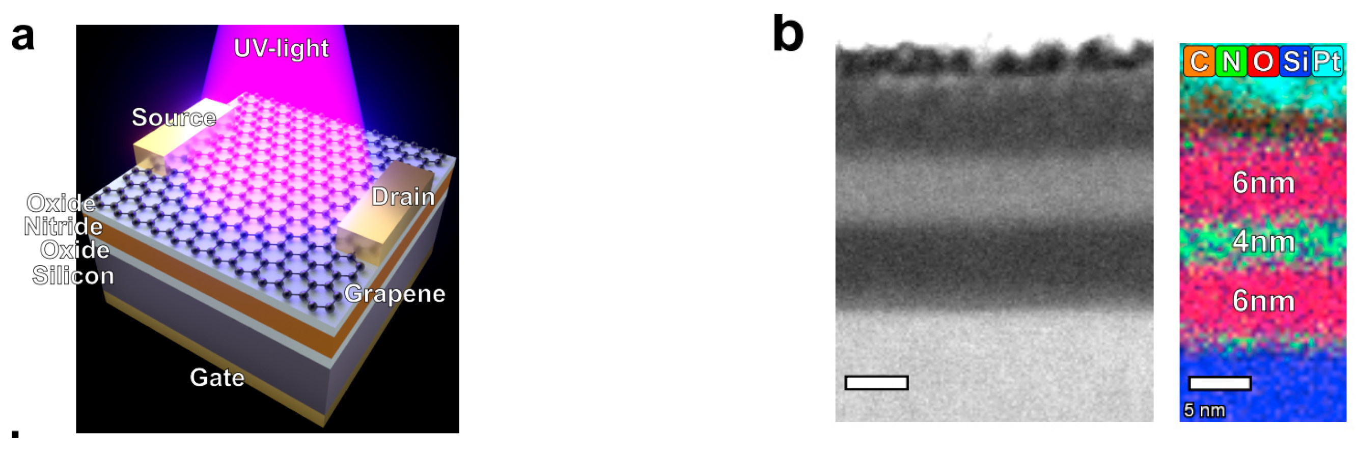
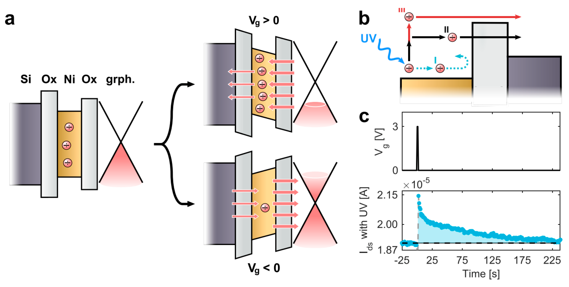
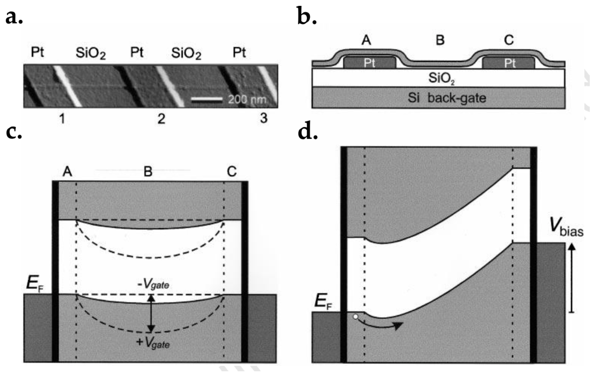
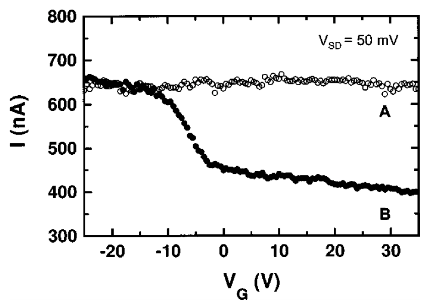
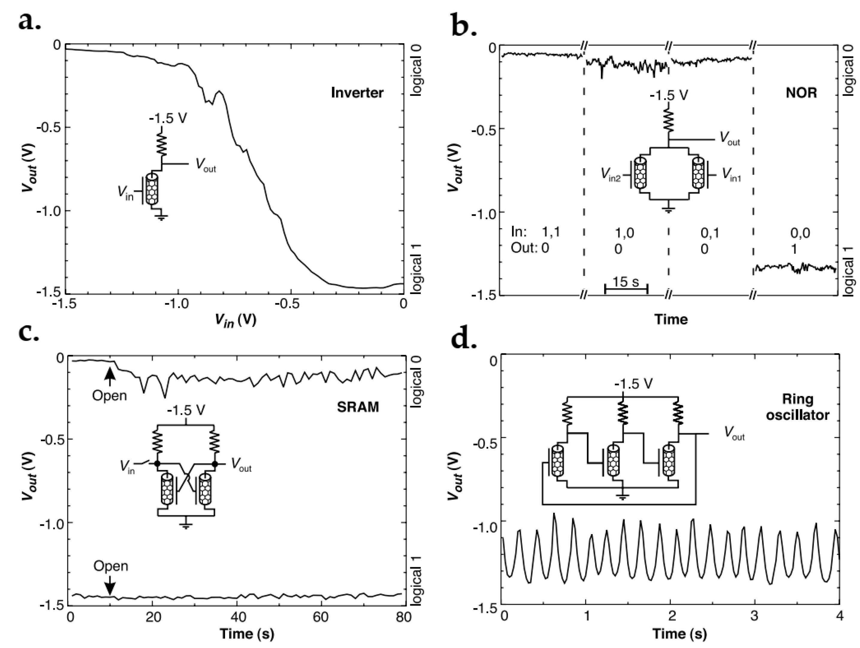
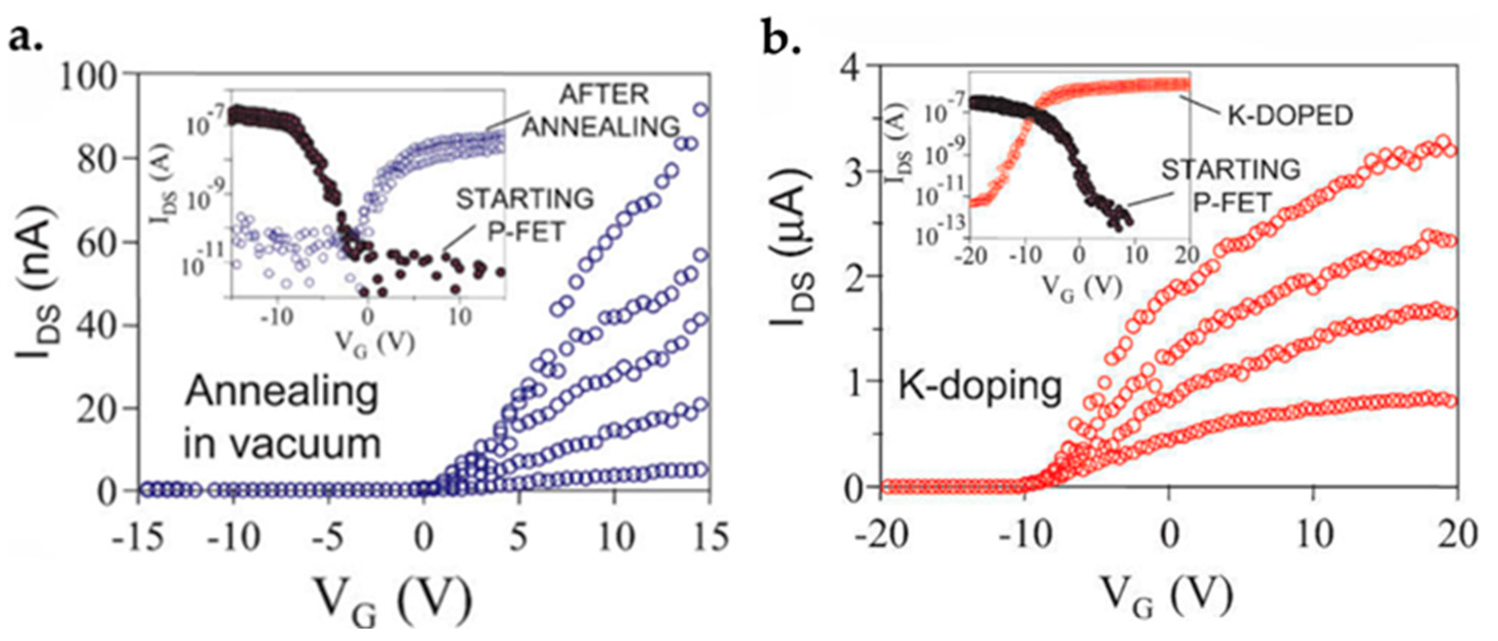
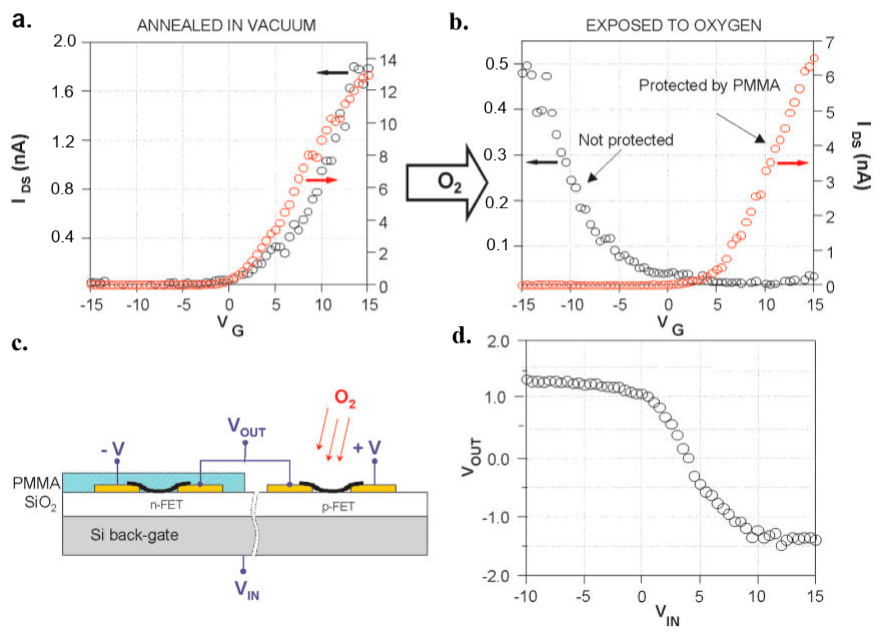
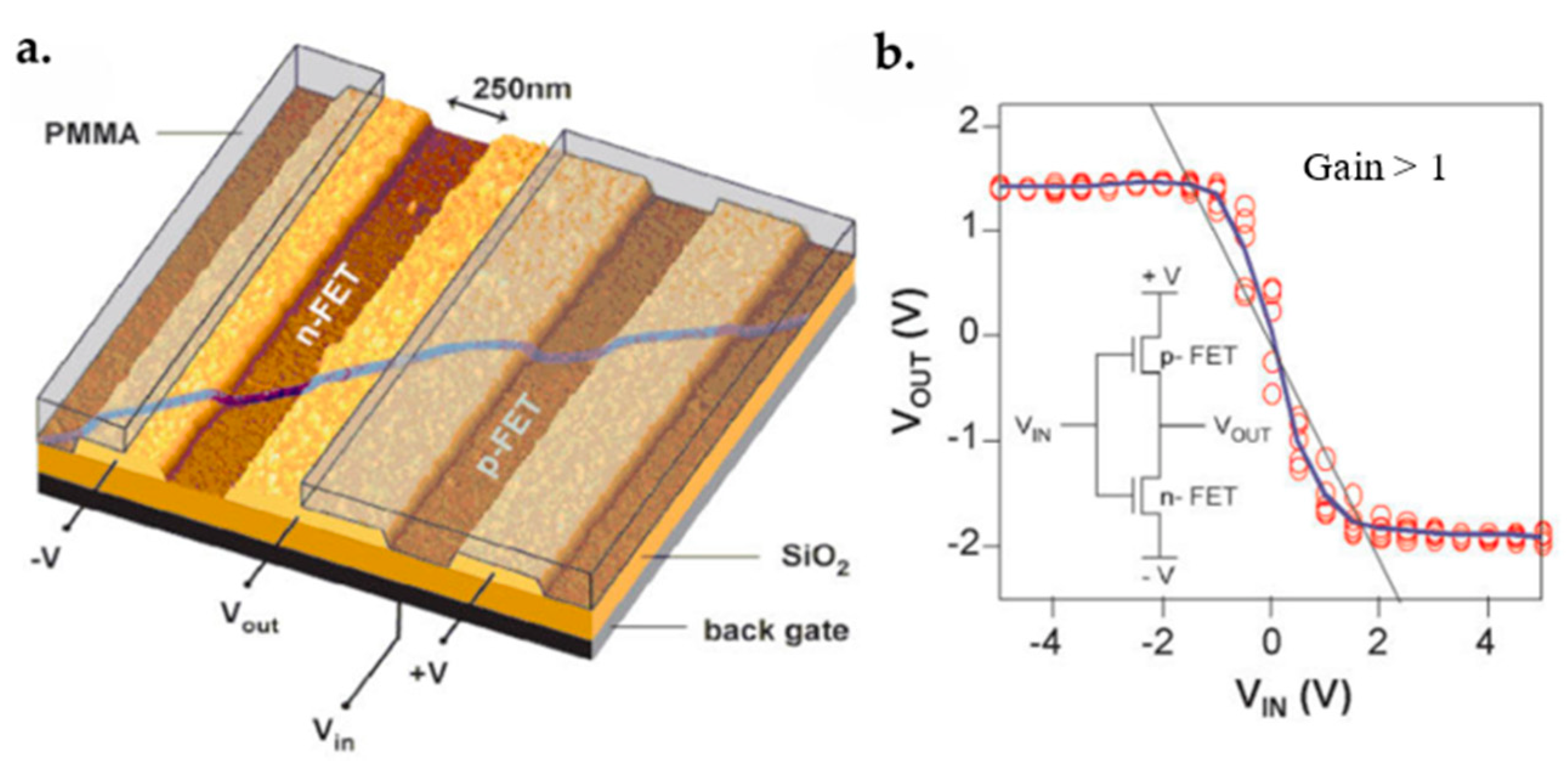
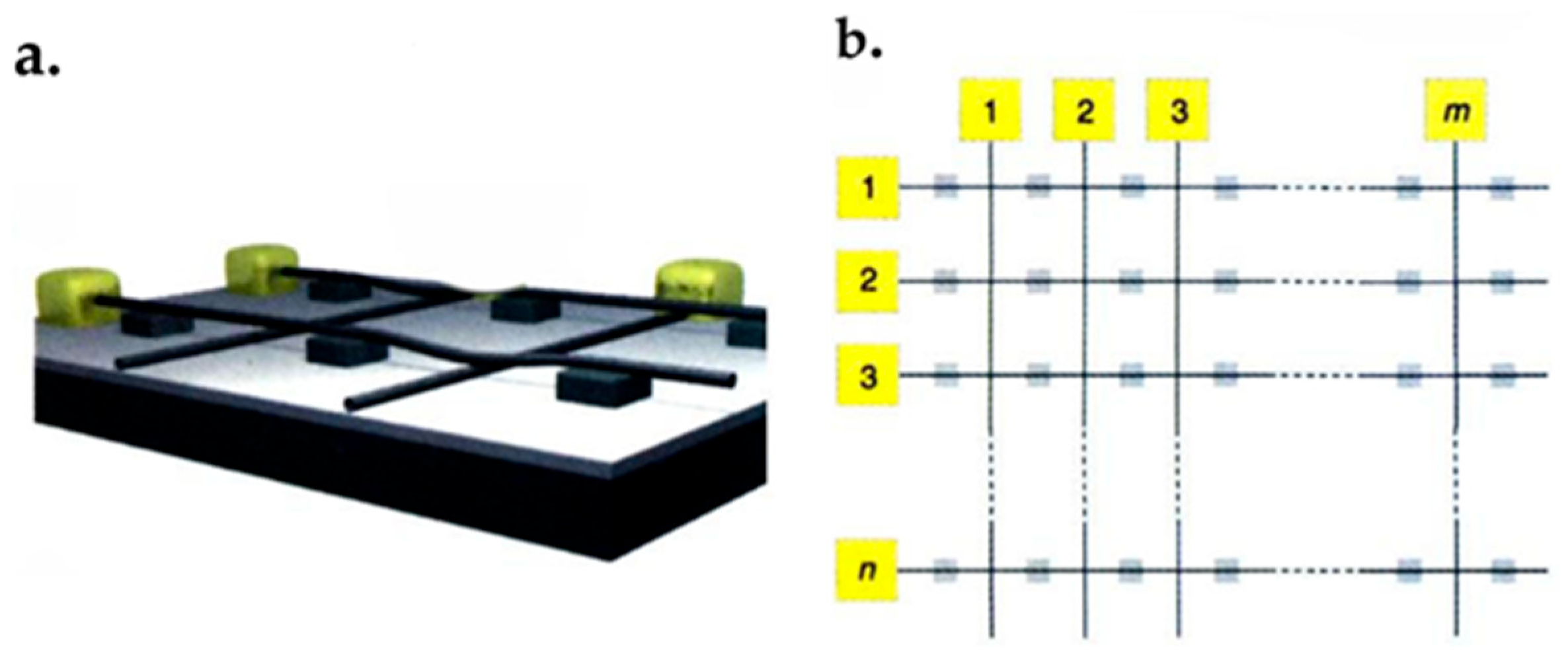
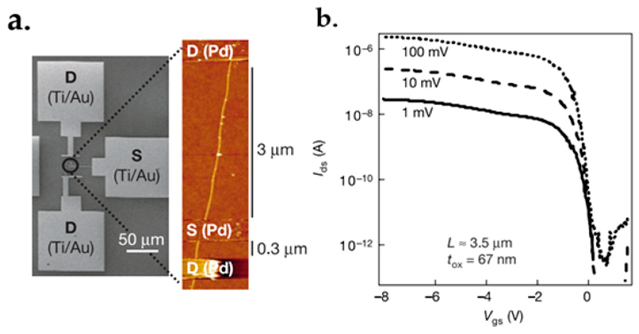
| (n1, n2) | (6,0) | (7,0) | (8,0) | (9,0) | (10,0) | (11,0) | (12,0) | (13,0) | (14,0) | (15,0) |
|---|---|---|---|---|---|---|---|---|---|---|
| Reference [70] (Eg eV) | 0.243 | 0.643 | 0.093 | 0.764 | 0.939 | 0.078 | 0.625 | 0.736 | 0.028 | |
| Reference [70] (Eg eV) | 0.21 | 1.0 | 1.22 | 0.045 | 0.86 | 0.89 | 0.008 | 0.679 | 0.7 | 0.0 |
| Reference [73] (Eg eV) | 0.79 | 1.12 | 0.65 | 0.80 | ||||||
| Reference [73] (Eg eV) | 1.11 | 1.33 | 0.87 | 0.96 | ||||||
| Reference [74] (TB) (Eg eV) | 0.05 | 1.04 | 1.19 | 0.07 | ||||||
| Reference [74] (LDA) (Eg eV) | Metal(−0.83) | 0.09 | 0.62 | 0.17 | ||||||
| Reference [75] B3LYP (Eg eV) | 0.00 | 0.079 | 0.041 | 0.036 | ||||||
| Reference [75] experimental (Eg eV) | 0.80 | 0.042 | 0.029 | |||||||
| Reference [75] LDA (Eg eV) | 0.024 | 0.002 | 0.00 |
| Method | Sources | Advantages | Disadvantages | References |
|---|---|---|---|---|
| Exfoliation | Graphite | Simple and high yielding | Not fully purified | [120,121,122,123] |
| Scotch-tape and drawing method | Graphite | Simple and high quality | Cannot be scaled further, limit in size | [119,124,125] |
| Sanitation | Graphite powder and flakes | High quality | Low production, time consumption | [126,127,128,129,130] |
| Reduction | Different carbon sourcesOther activated carbons | Large-area monolayer graphene films onto a variety of substrates | Limited in yield. | [131,132,133,134,135,136,137] |
| Epitaxy | Metal–carbon solutions or 6H-SiC | High quality, mono-/bi-/trilayer graphene | Requires expensive equipment, throughput issue and scaling requires significant effort | [144,145,146,147,148] |
| Chemical vapor deposition (CVD) | CH4 and C2H2 gases | High quality, large size, monolayer or bilayer graphene | Requires expensive equipment, throughput issue and scaling requires significant effortSome of the gaseous raw materials are hazardous, the use is limited in some applications and a concern for large-scale production | [149,150,151,152,153,154,155,156,157,158,159,160,161,162,163,164,165,166,167,168,169] |
| Synthesis Methods | Advantages | Disadvantages | References |
|---|---|---|---|
| Arc discharge | Mass production, SWCNTs and MWCNTs | Multi morphology | [4,11,180,181,182,183] |
| Laser ablation | SWCNTs yield with a controlling diameter distribution | Not suitable for mass production | [184] |
| Chemical vapordeposition (CVD) | Mass production | Modification process parameters needed to control SWCNTs diameter distribution and yield | [186,187,188,189,190] |
Publisher’s Note: MDPI stays neutral with regard to jurisdictional claims in published maps and institutional affiliations. |
© 2022 by the authors. Licensee MDPI, Basel, Switzerland. This article is an open access article distributed under the terms and conditions of the Creative Commons Attribution (CC BY) license (https://creativecommons.org/licenses/by/4.0/).
Share and Cite
Kolahdouz, M.; Xu, B.; Nasiri, A.F.; Fathollahzadeh, M.; Manian, M.; Aghababa, H.; Wu, Y.; Radamson, H.H. Carbon-Related Materials: Graphene and Carbon Nanotubes in Semiconductor Applications and Design. Micromachines 2022, 13, 1257. https://doi.org/10.3390/mi13081257
Kolahdouz M, Xu B, Nasiri AF, Fathollahzadeh M, Manian M, Aghababa H, Wu Y, Radamson HH. Carbon-Related Materials: Graphene and Carbon Nanotubes in Semiconductor Applications and Design. Micromachines. 2022; 13(8):1257. https://doi.org/10.3390/mi13081257
Chicago/Turabian StyleKolahdouz, Mohammadreza, Buqing Xu, Aryanaz Faghih Nasiri, Maryam Fathollahzadeh, Mahmoud Manian, Hossein Aghababa, Yuanyuan Wu, and Henry H. Radamson. 2022. "Carbon-Related Materials: Graphene and Carbon Nanotubes in Semiconductor Applications and Design" Micromachines 13, no. 8: 1257. https://doi.org/10.3390/mi13081257