
All-Solid-State Beam Steering via Integrated Optical Phased Array Technology

Abstract
:1. Introduction
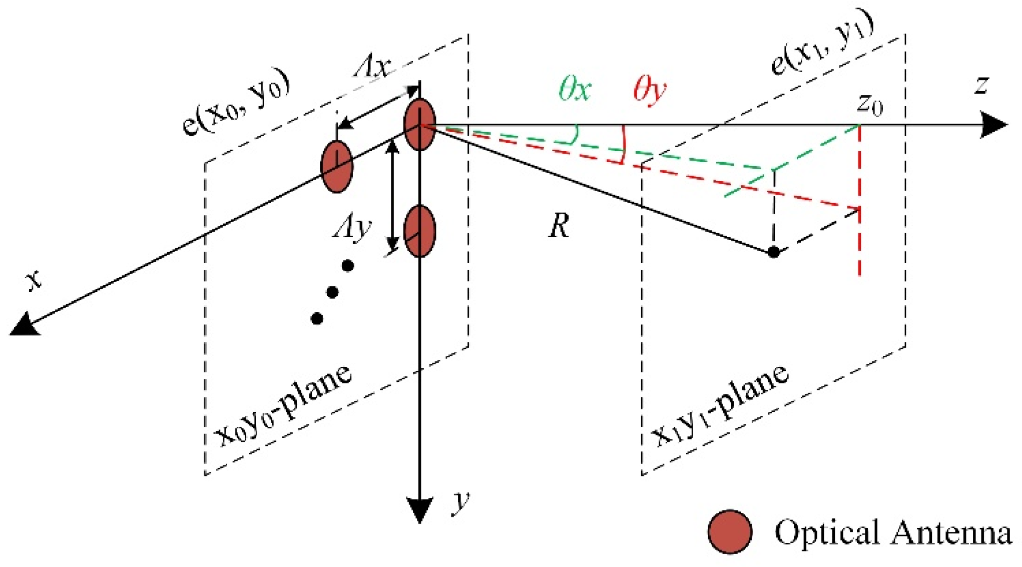
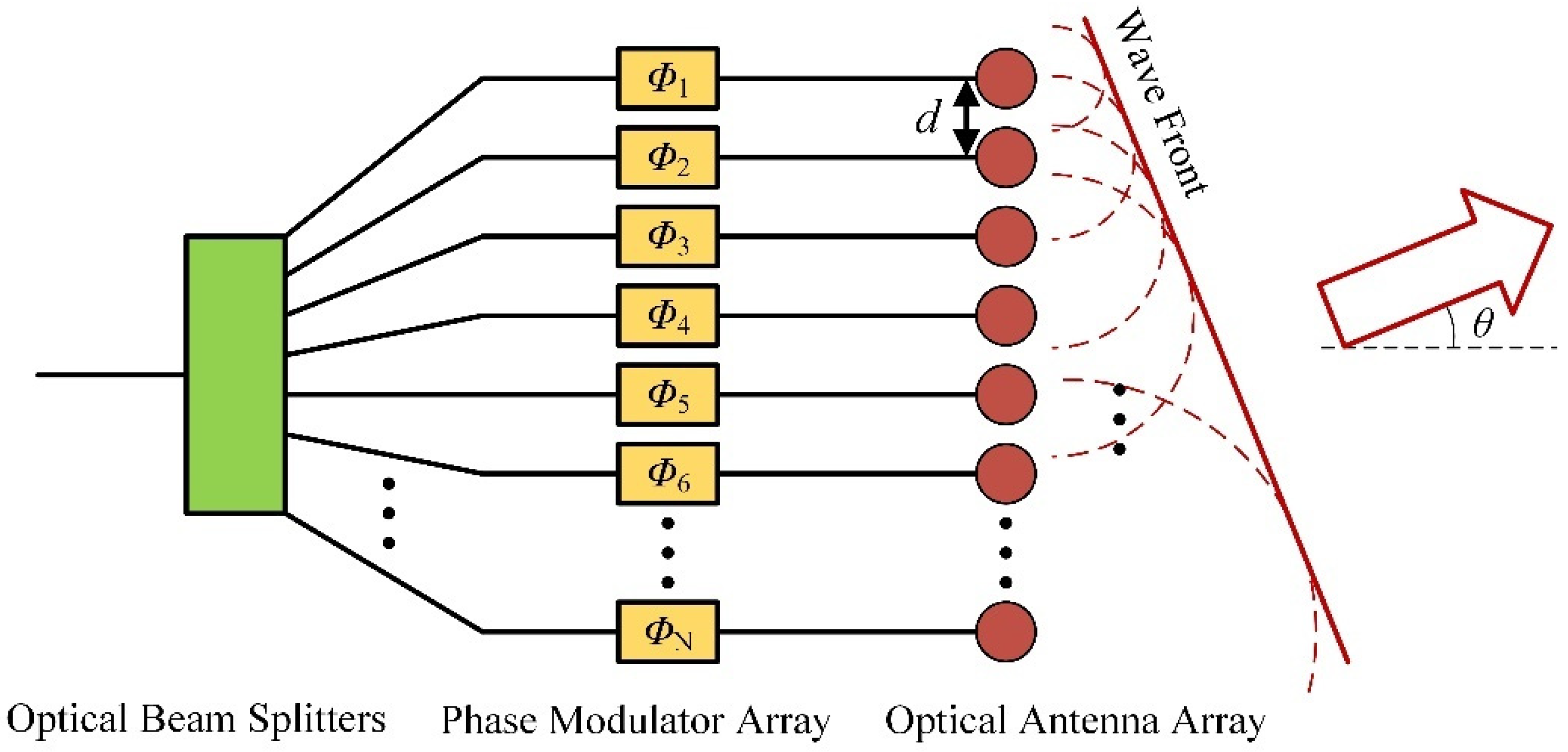
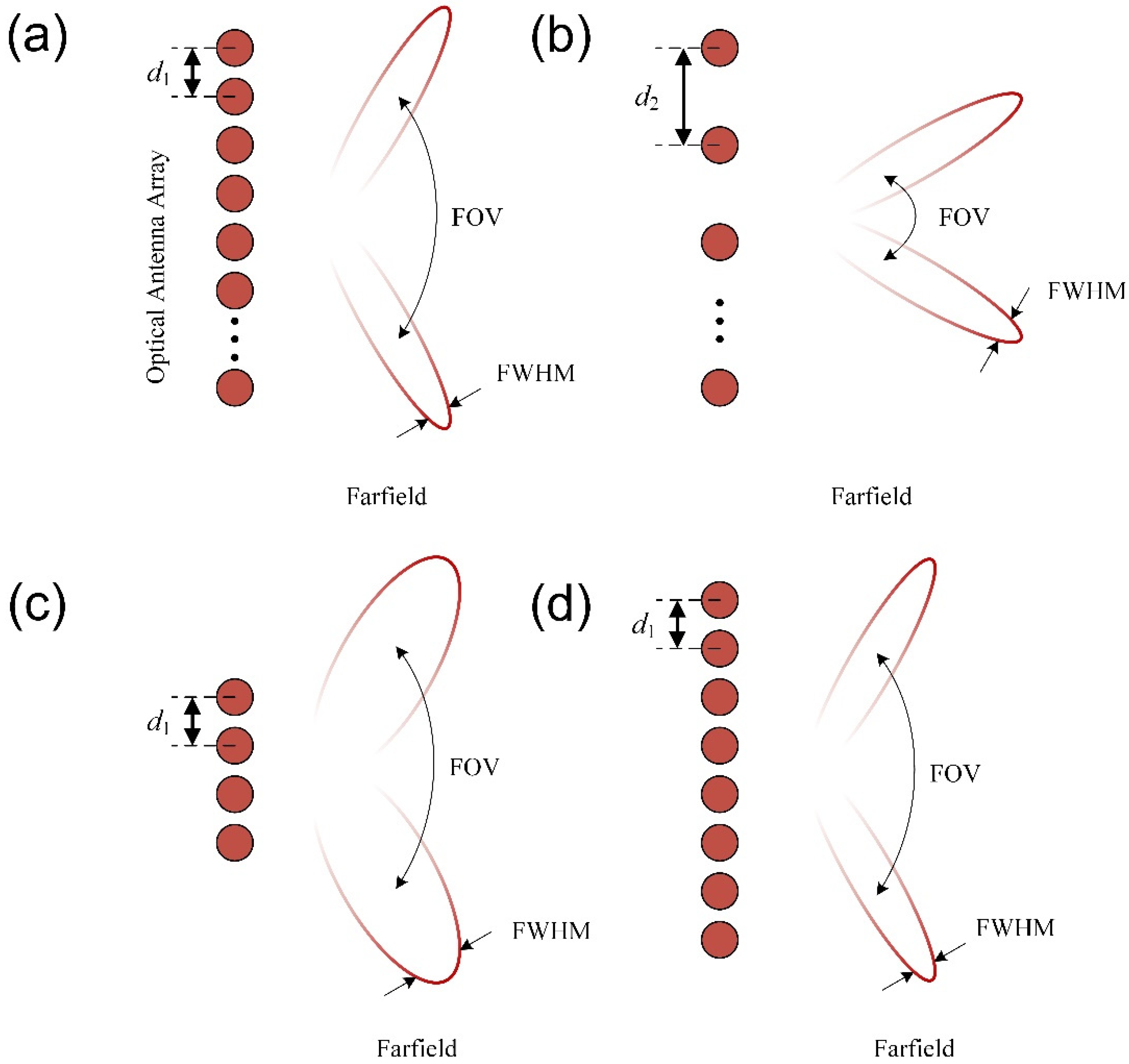
2. Principle
3. OPAs for Beam Steering
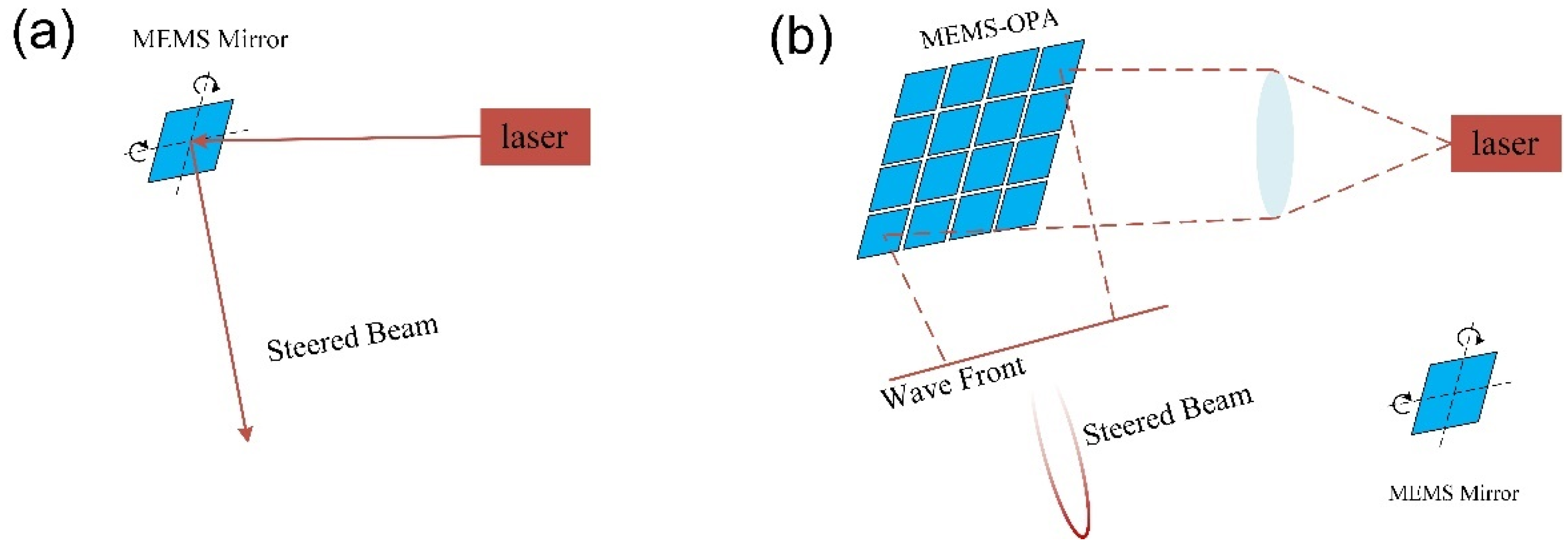
3.1. MEMS-OPA
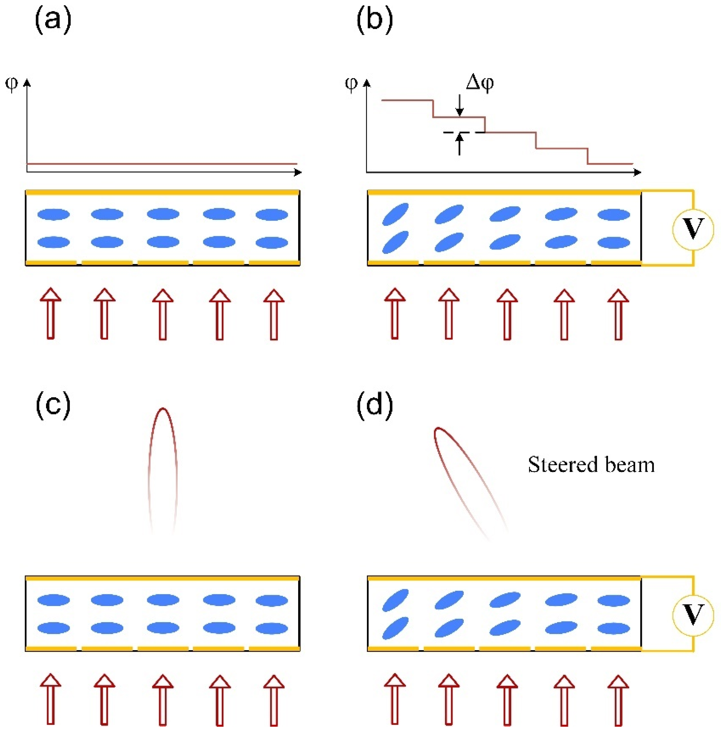
3.2. LC-OPA
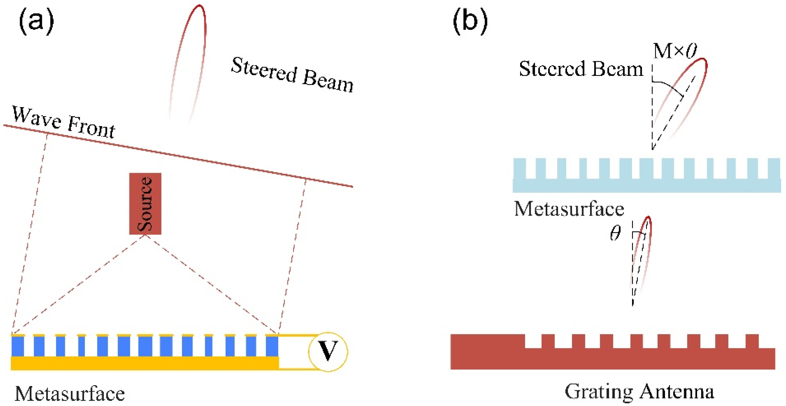
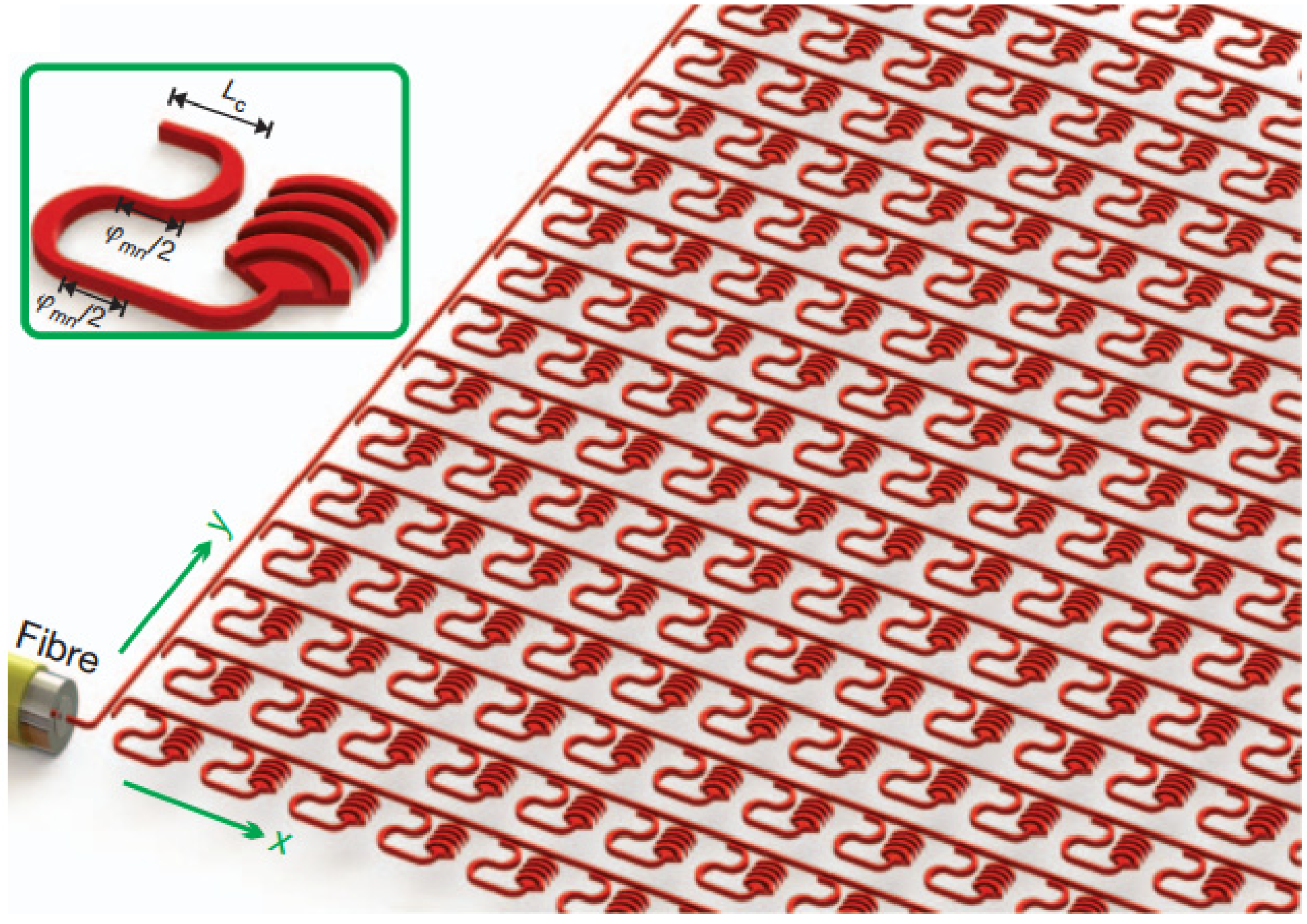
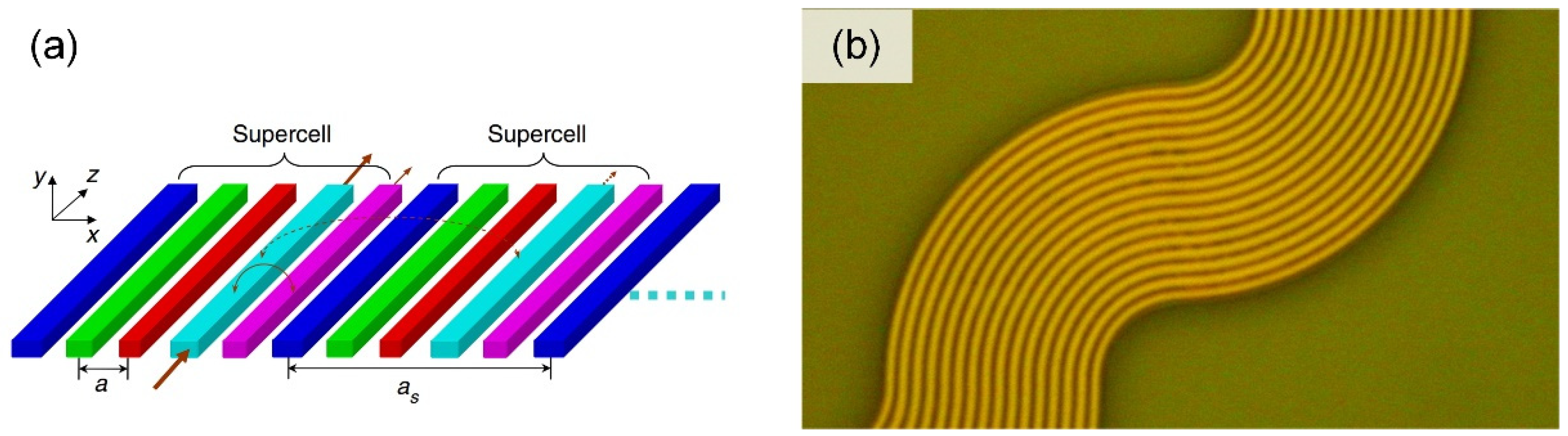
3.3. Meta-OPA
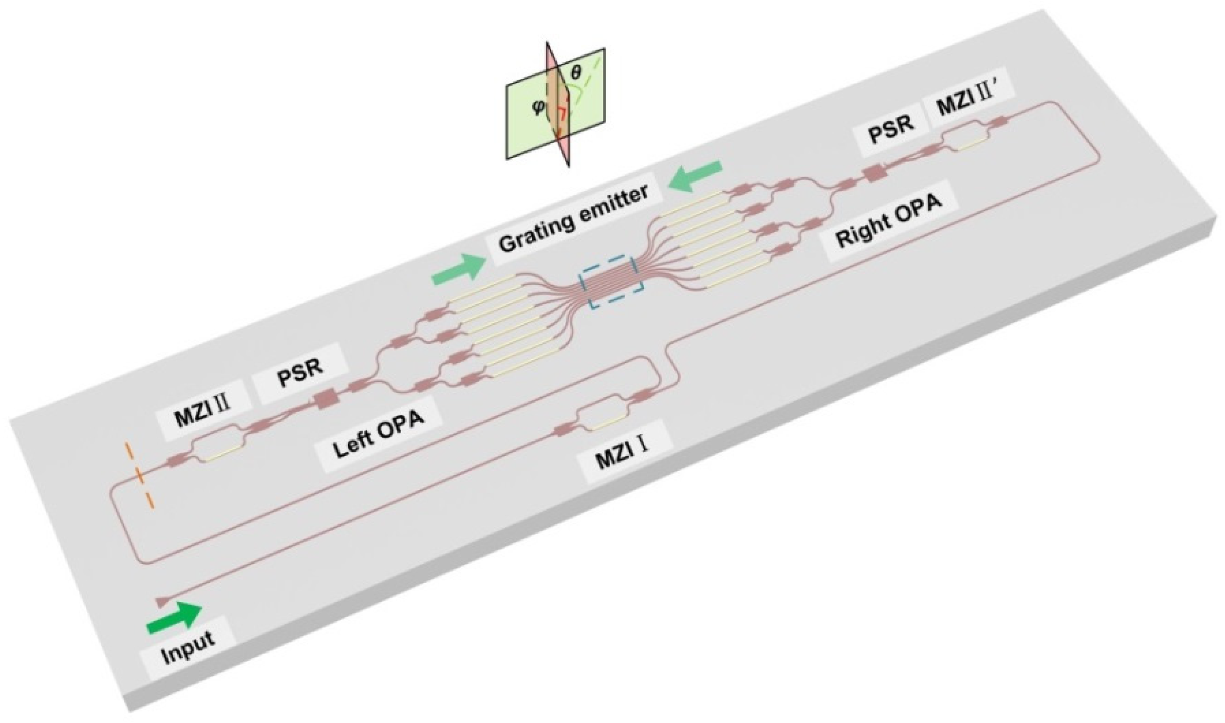
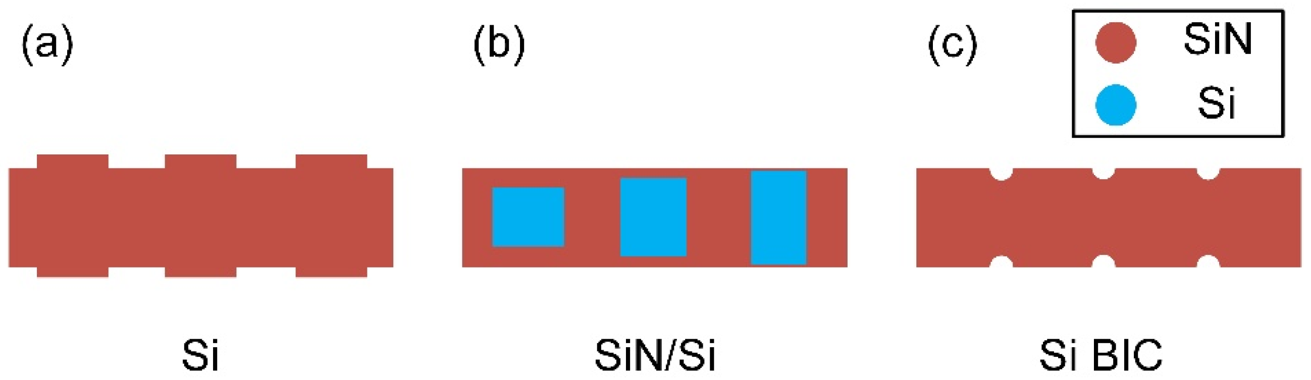
3.4. PIC-OPA
4. Discussion
Author Contributions
Funding
Conflicts of Interest
References
- Poulton, C.V.; Byrd, M.J.; Russo, P.; Timurdogan, E.; Khandaker, M.; Vermeulen, D.; Watts, M.R. Long-Range LiDAR and Free-Space Data Communication With High-Performance Optical Phased Arrays. IEEE J. Sel. Top. Quantum Electron. 2019, 25, 7700108. [Google Scholar] [CrossRef]
- Niclass, C.; Ito, K.; Soga, M.; Matsubara, H.; Aoyagi, I.; Kato, S.; Kagami, M. Design and characterization of a 256 × 64-pixel single-photon imager in CMOS for a MEMS-based laser scanning time-of-flight sensor. Opt. Express 2012, 20, 11863–11881. [Google Scholar] [CrossRef]
- McCarthy, A.; Ren, X.; Della Frera, A.; Gemmell, N.R.; Krichel, N.J.; Scarcella, C.; Ruggeri, A.; Tosi, A.; Buller, G.S. Kilometer-range depth imaging at 1550 nm wavelength using an InGaAs/InP single-photon avalanche diode detector. Opt. Express 2013, 21, 22098–22113. [Google Scholar] [CrossRef] [PubMed] [Green Version]
- Fernandez-Diaz, J.; Carter, W.; Shrestha, R.; Glennie, C. Now You See It… Now You Don’t: Understanding Airborne Mapping LiDAR Collection and Data Product Generation for Archaeological Research in Mesoamerica. Remote Sens. 2014, 6, 9951–10001. [Google Scholar] [CrossRef] [Green Version]
- Häne, C.; Heng, L.; Lee, G.H.; Fraundorfer, F.; Furgale, P.; Sattler, T.; Pollefeys, M. 3D visual perception for self-driving cars using a multi-camera system: Calibration, mapping, localization, and obstacle detection. Image Vis. Comput. 2017, 68, 14–27. [Google Scholar] [CrossRef] [Green Version]
- Zhuang, D.; Zhagn, L.; Han, X.; Li, Y.; Li, Y.; Liu, X.; Gao, F.; Song, J. Omnidirectional beam steering using aperiodic optical phased array with high error margin. Opt. Express 2018, 26, 19154–19170. [Google Scholar] [CrossRef] [PubMed]
- Guan, B.; Scott, R.P.; Qin, C.; Fontaine, N.K.; Su, T.; Ferrari, C.; Cappuzzo, M.; Klemens, F.; Keller, B.; Earnshaw, M.; et al. Free-space coherent optical communication with orbital angular, momentum multiplexing/demultiplexing using a hybrid 3D photonic integrated circuit. Opt. Express 2014, 22, 145–156. [Google Scholar] [CrossRef] [Green Version]
- Wang, D.; Watkins, C.; Xie, H. MEMS Mirrors for LiDAR: A review. Micromachines 2020, 11, 456. [Google Scholar] [CrossRef]
- Liu, J.; Sun, Q.; Fan, Z.; Jia, Y. TOF Lidar Development in Autonomous Vehicle. In Proceedings of the 2018 IEEE 3rd Optoelectronics Global Conference (OGC), Piscataway, NJ, USA, 4–7 September 2018; Volume 5. [Google Scholar]
- Kim, T.; Ngai, T.; Timalsina, Y.; Watts, M.R.; Stojanovic, V.; Bhargava, P.; Poulton, C.V.; Notaros, J.; Yaacobi, A.; Timurdogan, E.; et al. A Single-Chip Optical Phased Array in a Wafer-Scale Silicon Photonics/CMOS 3D-Integration Platform. IEEE J. Sel. Top. Quantum Electron. 2019, 54, 3061–3074. [Google Scholar] [CrossRef]
- Vaughan, O. RoboBee breaks free. Nat. Electron. 2019, 2, 265. [Google Scholar] [CrossRef]
- Goodman, J.W. Introduction to Fourier Optics, 2nd ed.; McGraw-Hill, Inc.: New York, NY, USA, 1996; pp. 74–75. [Google Scholar]
- Acoleyen, K.V. Nanophotonic Beam Steering Elements Using Silicon Technology for Wireless Optical Applications. Ph.D. Thesis, Ghent University, Ghent, Belgium, 2012. [Google Scholar]
- Van Acoleyen, K.; Bogaerts, W.; Jágerská, J.; Le Thomas, N.; Houdré, R.; Baets, R. Off-chip beam steering with a one-dimensional optical phased array on silicon-on-insulator. Opt. Lett. 2009, 34, 1477–1479. [Google Scholar] [CrossRef] [PubMed]
- Van Acoleyen, K.; Rogier, H.; Baets, R. Two-dimensional optical phased array antenna on silicon-on-insulator. Opt. Express 2010, 18, 13655–13660. [Google Scholar] [CrossRef] [PubMed] [Green Version]
- Chung, S.; Abediasl, H.; Hashemi, H. A Monolithically Integrated Large-Scale Optical Phased Array in Silicon-on-Insulator CMOS. IEEE J. Solid-State Circuit 2018, 53, 275–296. [Google Scholar] [CrossRef]
- Midkiff, J.; Yoo, K.M.; Shin, J.-D.; Dalir, H.; Teimourpour, M.; Chen, R.T. Optical phased array beam steering in the mid-infrared on an InP-based platform. Optica 2020, 7, 1544–1547. [Google Scholar] [CrossRef]
- Roriz, R.; Cabral, J.; Gomes, T. Automotive LiDAR Technology: A Survey. IEEE Trans. Intell. Transp. Syst. 2021, 1–16. [Google Scholar] [CrossRef]
- Lambert, J.; Carballo, A.; Cano, A.M.; Narksri, P.; Wong, D.; Takeuchi, E.; Takeda, K. Performance Analysis of 10 Models of 3D LiDARs for Automated Driving. IEEE Access 2020, 8, 131699–131722. [Google Scholar] [CrossRef]
- Bogatscher, S.; Streck, A.; Fox, M.; Meinzer, S.; Heussner, N.; Stork, W. Large aperture at low cost three-dimensional time-of-flight range sensor using scanning micromirrors and synchronous detector switching. Appl. Opt. 2014, 53, 1570–1582. [Google Scholar] [CrossRef]
- Walker, J.A. Future of MEMS in telecommunications networks. J. Micromech. Microeng. 2000, 10, R1. [Google Scholar] [CrossRef]
- Lee, C.; Kim, J.Y.; Kim, C. Recent Progress on Photoacoustic Imaging Enhanced with Microelectromechanical Systems (MEMS) Technologies. Micromachines 2018, 9, 584. [Google Scholar] [CrossRef] [Green Version]
- Errando-Herranz, C.; Takabayashi, A.Y.; Edinger, P.; Sattari, H.; Gylfason, K.B.; Quack, N. MEMS for Photonic Integrated Circuits. IEEE J. Sel. Top. Quantum Electron. 2020, 26, 8200916. [Google Scholar] [CrossRef] [Green Version]
- Yingshun, X.; Singh, J.; Selvaratnam, T.; Nanguang, C. Two-Axis Gimbal-Less Electrothermal Micromirror for Large-Angle Circumferential Scanning. IEEE J. Sel. Top. Quantum Electron. 2009, 15, 1432–1438. [Google Scholar] [CrossRef]
- Hofmann, U.; Janes, J.; Quenzer, H.-J. High-Q MEMS Resonators for Laser Beam Scanning Displays. Micromachines 2012, 3, 509–528. [Google Scholar] [CrossRef]
- Urey, H. MEMS scanners for display and imaging applications. In Proceedings of the Optomechatronic Micro/Nano Components, Devices, and Systems, Philadelphia, PA, USA, 25 October 2004. [Google Scholar]
- Zhu, Y.; Liu, W.; Jia, K.; Liao, W.; Xie, H. A piezoelectric unimorph actuator based tip-tilt-piston micromirror with high fill factor and small tilt and lateral shift. Sens. Actuator A Phys. 2011, 167, 495–501. [Google Scholar] [CrossRef]
- Holmstrom, S.T.S.; Baran, U.; Urey, H. MEMS Laser Scanners: A Review. J. Microelectromech. Syst. 2014, 23, 259–275. [Google Scholar] [CrossRef]
- Jung, I.W.; Krishnamoorthy, U.; Solgaard, O. High Fill-Factor Two-Axis Gimbaled Tip-Tilt-Piston Micromirror Array Actuated by Self-Aligned Vertical Electrostatic Combdrives. J. Microelectromech. Syst. 2006, 15, 563–571. [Google Scholar] [CrossRef]
- Megens, M.; Yoo, B.W.; Chan, T.; Yang, W.; Horsley, D.A. High-contrast grating mems optical phase-shifters for two-dimensional free-space beam steering. Proc. SPIE Int. Soc. Opt. Eng. 2014, 8995, 2978–2982. [Google Scholar]
- Wang, Y.; Zhou, G.; Zhang, X.; Kwon, K.; Blanche, P.-A.; Triesault, N.; Yu, K.-S.; Wu, M.C. 2D broadband beamsteering with large-scale MEMS optical phased array. Optica 2019, 6, 557–562. [Google Scholar] [CrossRef] [Green Version]
- Yang, W.; Sun, T.; Rao, Y.; Megens, M.; Chan, T.; Yoo, B.W.; Horsley, D.A.; Wu, M.C.; Chang-Hasnain, C.J. High speed optical phased array using high contrast grating all-pass filters. Opt. Express 2014, 22, 20038–20044. [Google Scholar] [CrossRef]
- Mcmanamon, P.F.; Dorschner, T.A. Optical phased array technology. Proc. IEEE 1996, 84, 268–298. [Google Scholar] [CrossRef]
- Qin, S.; Liu, C.; Wang, J.; Chen, K.; Xu, J.; Fu, S.; Liu, D.; Ran, Y. Liquid crystal-optical phased arrays (LC-OPA)-based optical beam steering with microradian resolution enabled by double gratings. Appl. Opt. 2019, 58, 4091–4098. [Google Scholar] [CrossRef]
- Morris, R.; Jones, J.C.; Nagaraj, M. Liquid Crystal Devices for Beam Steering Applications. Micromachines 2021, 12, 247. [Google Scholar] [CrossRef] [PubMed]
- Hosseini, A.; Kwong, D.; Yang, Z.; Yun-Sheng, C.; Crnogorac, F.; Pease, R.F.W.; Chen, R.T. Unequally Spaced Waveguide Arrays for Silicon Nanomembrane-Based Efficient Large Angle Optical Beam Steering. IEEE J. Sel. Top. Quantum Electron. 2009, 15, 1439–1446. [Google Scholar] [CrossRef]
- Engström, D.; O’Callaghan, M.J.; Walker, C.; Handschy, M.A. Fast beam steering with a ferroelectric-liquid-crystal optical phased array. Appl. Opt. 2009, 48, 5. [Google Scholar] [CrossRef] [PubMed]
- Wang, X.; Tan, Q.; Huang, Z.; Tang, Z. Liquid crystal optical phased array device with a fine steering precision of a few micro-radians. Opt. Commun. 2014, 313, 360–364. [Google Scholar] [CrossRef]
- Chang, C.; Bang, K.; Wetzstein, G.; Lee, B.; Gao, L. Toward the next-generation VR/AR optics: A review of holographic near-eye displays from a human-centric perspective. Optica 2020, 7, 1563–1578. [Google Scholar] [CrossRef]
- Khorasaninejad, M.; Chen, W.T.; Devlin, R.C.; Oh, J.; Zhu, A.Y.; Capasso, F. Metalenses at visible wavelengths: Diffraction-limited focusing and subwavelength resolution imaging. Science 2016, 352, 1190–1194. [Google Scholar] [CrossRef] [Green Version]
- Jin, L.; Huang, Y.W.; Jin, Z.; Devlin, R.C.; Dong, Z.; Mei, S.; Jiang, M.; Chen, W.T.; Wei, Z.; Liu, H.; et al. Dielectric multi-momentum meta-transformer in the visible. Nat. Commun. 2019, 10, 4789. [Google Scholar] [CrossRef] [Green Version]
- Ai, H.; Kang, Q.; Wang, W.; Guo, K.; Guo, Z. Multi-Beam Steering for 6G Communications Based on Graphene Metasurfaces. Sensors 2021, 21, 4784. [Google Scholar] [CrossRef]
- Wang, W.; Zhao, R.; Chang, S.; Li, J.; Shi, Y.; Liu, X.; Sun, J.; Kang, Q.; Guo, K.; Guo, Z. High-Efficiency Spin-Related Vortex Metalenses. Nanomaterials 2021, 11, 1485. [Google Scholar] [CrossRef]
- Park, J.; Jeong, B.G.; Kim, S.I.; Lee, D.; Kim, J.; Shin, C.; Lee, C.B.; Otsuka, T.; Kyoung, J.; Kim, S.; et al. All-solid-state spatial light modulator with independent phase and amplitude control for three-dimensional LiDAR applications. Nat. Nanotechnol. 2021, 16, 69–76. [Google Scholar] [CrossRef]
- Guo, K.; Li, X.; Ai, H.; Ding, X.; Wang, L.; Wang, W.; Guo, Z. Tunable oriented mid-infrared wave based on metasurface with phase change material of GST. Results Phys. 2022, 34, 105269. [Google Scholar] [CrossRef]
- Ding, X.; Kang, Q.; Guo, K.; Guo, Z. Tunable GST metasurfaces for chromatic aberration compensation in the mid-infrared. Opt. Mater. 2020, 109, 110284. [Google Scholar] [CrossRef]
- Arbabi, A.; Arbabi, E.; Kamali, S.M.; Horie, Y.; Han, S.; Faraon, A. Miniature optical planar camera based on a wide-angle metasurface doublet corrected for monochromatic aberrations. Nat. Commun. 2016, 7, 13682. [Google Scholar] [CrossRef] [PubMed]
- Zhou, C.; Lee, W.B.; Park, C.S.; Gao, S.; Choi, D.Y.; Lee, S.S. Multifunctional Beam Manipulation at Telecommunication Wavelengths Enabled by an All-Dielectric Metasurface Doublet. Adv. Opt. Mater. 2020, 8, 2000645. [Google Scholar] [CrossRef]
- Lee, W.-B.; Im, C.-S.; Zhou, C.; Bhandari, B.; Choi, D.-Y.; Lee, S.-S. Metasurface doublet-integrated bidirectional grating antenna enabling enhanced wavelength-tuned beam steering. Photonics Res. 2021, 10, 248–255. [Google Scholar] [CrossRef]
- Notaros, J.; Watts, M.R.; Li, N.; Poulton, C.V.; Su, Z.; Byrd, M.J.; Magden, E.S.; Timurdogan, E.; Baiocco, C.; Fahrenkopf, N.M. CMOS-Compatible Optical Phased Array Powered by a Monolithically-Integrated Erbium Laser. J. Lightwave Technol. 2019, 37, 5982–5987. [Google Scholar] [CrossRef]
- Doylend, J.K.; Heck, M.J.R.; Bovington, J.T.; Peters, J.D.; Davenport, M.L.; Coldren, L.A.; Bowers, J.E. Hybrid III/V silicon photonic source with integrated 1D free-space beam steering. Opt. Lett. 2012, 37, 4257–4259. [Google Scholar] [CrossRef]
- Hulme, J.C.; Doylend, J.K.; Heck, M.J.; Peters, J.D.; Davenport, M.L.; Bovington, J.T.; Coldren, L.A.; Bowers, J.E. Fully integrated hybrid silicon two dimensional beam scanner. Opt. Express 2015, 23, 5861–5874. [Google Scholar] [CrossRef]
- Liu, S.; Feng, J.; Tian, Y.; Zhao, H.; Jin, L.; Ouyang, B.; Zhu, J.; Guo, J. Thermo-optic phase shifters based on silicon-on-insulator platform: State-of-the-art and a review. Front. Optoelectron. 2022, 15, 9. [Google Scholar] [CrossRef]
- Im, C.-S.; Kim, S.-M.; Lee, K.-P.; Ju, S.-H.; Hong, J.-H.; Yoon, S.-W.; Kim, T.; Lee, E.-S.; Bhandari, B.; Zhou, C.; et al. Hybrid Integrated Silicon Nitride–Polymer Optical Phased Array For Efficient Light Detection and Ranging. J. Lightwave Technol. 2021, 39, 4402–4409. [Google Scholar] [CrossRef]
- Kim, S.H.; You, J.B.; Ha, Y.G.; Kang, G.; Lee, D.S.; Yoon, H.; Yoo, D.E.; Lee, D.W.; Yu, K.; Youn, C.H.; et al. Thermo-optic control of the longitudinal radiation angle in a silicon-based optical phased array. Opt. Lett. 2019, 44, 411–414. [Google Scholar] [CrossRef] [PubMed]
- Meyer, R.A. Optical beam steering using a multichannel lithium tantalate crystal. Appl. Opt. 1972, 11, 613–616. [Google Scholar] [CrossRef] [PubMed]
- Komatsu, K.; Kohno, Y.; Nakano, Y.; Tanemura, T. Large-Scale Monolithic InP-Based Optical Phased Array. IEEE Photonics Technol. Lett. 2021, 33, 1123–1126. [Google Scholar] [CrossRef]
- Guo, W.; Binetti, P.R.A.; Althouse, C.; Masanovic, M.L.; Ambrosius, H.P.M.M.; Johansson, L.A.; Coldren, L.A. Two-Dimensional Optical Beam Steering with InP-Based Photonic Integrated Circuits. IEEE J. Sel. Top. Quantum Electron. 2013, 19, 6100212. [Google Scholar] [CrossRef]
- Xie, W.; Komljenovic, T.; Huang, J.; Tran, M.; Davenport, M.; Torres, A.; Pintus, P.; Bowers, J. Heterogeneous silicon photonics sensing for autonomous cars. Opt. Express 2019, 27, 3642–3663. [Google Scholar] [CrossRef]
- Liu, J.; Lucas, E.; Raja, A.S.; He, J.; Riemensberger, J.; Wang, R.N.; Karpov, M.; Guo, H.; Bouchand, R.; Kippenberg, T.J. Photonic microwave generation in the X- and K-band using integrated soliton microcombs. Nat. Photonics 2020, 14, 486–491. [Google Scholar] [CrossRef]
- Zhang, L.; Li, Y.; Hou, Y.; Wang, Y.; Tao, M.; Chen, B.; Na, Q.; Li, Y.; Zhi, Z.; Liu, X.; et al. Investigation and demonstration of a high-power handling and large-range steering optical phased array chip. Opt. Express 2021, 29, 29755–29765. [Google Scholar] [CrossRef]
- Wang, H.; Chen, Z.; Sun, C.; Deng, S.; Tang, X.; Zhang, L.; Jiang, R.; Shi, W.; Chen, Z.; Li, Z.; et al. Broadband silicon nitride nanophotonic phased arrays for wide-angle beam steering. Opt. Lett. 2021, 46, 286–289. [Google Scholar] [CrossRef]
- Tyler, N.A.; Fowler, D.; Malhouitre, S.; Garcia, S.; Grosse, P.; Rabaud, W.; Szelag, B. SiN integrated optical phased arrays for two-dimensional beam steering at a single near-infrared wavelength. Opt. Express 2019, 27, 5851–5858. [Google Scholar] [CrossRef]
- Poulton, C.V.; Byrd, M.J.; Raval, M.; Su, Z.; Li, N.; Timurdogan, E.; Coolbaugh, D.; Vermeulen, D.; Watts, M.R. Large-scale silicon nitride nanophotonic phased arrays at infrared and visible wavelengths. Opt. Lett. 2017, 42, 21–24. [Google Scholar] [CrossRef]
- Lipson, M. Guiding, modulating, and emitting light on Silicon-challenges and opportunities. J. Lightwave Technol. 2005, 23, 4222–4238. [Google Scholar] [CrossRef]
- Soref, R. The Past, Present, and Future of Silicon Photonics. IEEE J. Sel. Top. Quantum Electron. 2006, 12, 1678–1687. [Google Scholar] [CrossRef]
- Luo, L.W.; Ophir, N.; Chen, C.P.; Gabrielli, L.H.; Poitras, C.B.; Bergmen, K.; Lipson, M. WDM-compatible mode-division multiplexing on a silicon chip. Nat. Commun. 2014, 5, 3069. [Google Scholar] [CrossRef] [PubMed] [Green Version]
- Dai, D.; Bowers, J.E. Silicon-based on-chip multiplexing technologies and devices for Peta-bit optical interconnects. Nanophotonics 2014, 3, 283–311. [Google Scholar] [CrossRef]
- Sun, J.; Timurdogan, E.; Yaacobi, A.; Hosseini, E.S.; Watts, M.R. Large-scale nanophotonic phased array. Nature 2013, 493, 195–199. [Google Scholar] [CrossRef]
- Sun, J.; Hosseini, E.; Yaacobi, A.; Cole, D.B.; Leake, G.; Coolbaugh, D.; Watts, M.R. Two-dimensional apodized silicon photonic phased arrays. Opt. Lett. 2014, 39, 367–370. [Google Scholar] [CrossRef]
- Fatemi, R.; Khachaturian, A.; Hajimiri, A. A Nonuniform Sparse 2-D Large-FOV Optical Phased Array with a Low-Power PWM Drive. IEEE J. Solid-State Circuit 2019, 54, 1200–1215. [Google Scholar] [CrossRef]
- Ashtiani, F.; Aflatouni, F. N × N optical phased array with 2N phase shifters. Opt. Express 2019, 27, 27183–27190. [Google Scholar] [CrossRef]
- Song, W.; Gatdula, R.; Abbaslou, S.; Lu, M.; Stein, A.; Lai, W.Y.; Provine, J.; Pease, R.F.; Christodoulides, D.N.; Jiang, W. High-density waveguide superlattices with low crosstalk. Nat. Commun. 2015, 6, 7027. [Google Scholar] [CrossRef]
- Phare, C.T.; Min, C.S.; Miller, S.A.; Stern, B.; Lipson, M. Silicon optical phased array with high-efficiency beam formation over 180 degree field of view. In Proceedings of the Conference on Lasers Electro-Optics (CLEO), San Jose, CA, USA, 13–18 May 2018. Paper SM3I.2. [Google Scholar]
- Chen, J.; Sun, Y.; Wei, S.; Han, X.; Shi, Y. Optical phased array based on silicon waveguides with non-uniform widths. In Proceedings of the 23rd Opto-Electronics and Communications Conference, Seogwipo, Korea, 2–6 July 2018. [Google Scholar]
- Xu, H.; Shi, Y. Ultra-broadband 16-channel mode division (de)multiplexer utilizing densely packed bent waveguide arrays. Opt. Lett. 2016, 41, 4815–4818. [Google Scholar] [CrossRef]
- Yi, X.; Zhang, Y.; Zeng, H.; Gao, S.; Guo, S.; Qiu, C. Demonstration of an Ultra-compact 8-channel sinusoidal silicon waveguide array for optical phased array. Opt. Lett. 2022, 47, 226–229. [Google Scholar] [CrossRef] [PubMed]
- Chen, X.; Liu, W.; Zhang, Y.; Shi, Y. Polarization-insensitive broadband 2 × 2 3 dB power splitter based on silicon-bent directional couplers. Opt. Lett. 2017, 42, 3738–3740. [Google Scholar] [CrossRef] [PubMed]
- Zhao, S.; Liu, W.; Chen, J.; Ding, Z.; Shi, Y. Broadband Arbitrary Ratio Power Splitters Based on Directional Couplers with Subwavelength Structure. IEEE Photonics Technol. Lett. 2021, 33, 479–482. [Google Scholar] [CrossRef]
- Wang, P.; Luo, G.; Xu, Y.; Li, Y.; Su, Y.; Ma, J.; Wang, R.; Yang, Z.; Zhou, X.; Zhang, Y.; et al. Design and fabrication of a SiN-Si dua-layer optical phased array chip. Photonics Res. 2020, 8, 912–919. [Google Scholar] [CrossRef]
- Zhang, L.; Li, Y.; Tao, M.; Wang, Y.; Hou, Y.; Chen, B.; Li, Y.; Qin, L.; Gao, F.; Luo, X.; et al. Large-Scale Integrated Multi-Lines Optical Phased Array Chip. IEEE Photonics J. 2020, 12, 6601208. [Google Scholar] [CrossRef]
- Dai, D.; Li, C.; Wang, S.; Wu, H.; Shi, Y.; Wu, Z.; Gao, S.; Dai, T.; Yu, H.; Tsang, H.-K. 10-Channel Mode (de)multiplexer with Dual Polarizations. Laser Photonics Rev. 2018, 12, 1700109. [Google Scholar] [CrossRef]
- Chen, J.; Shi, Y. Flat-Top CWDM (De)Multiplexers Based on Contra-Directional Couplers with Subwavelength Gratings. IEEE Photonics Technol. Lett. 2019, 31, 2003–2006. [Google Scholar] [CrossRef]
- Yan, X.; Chen, J.; Dai, D.; Shi, Y. Polarization Multiplexing Silicon-Photonic Optical Phased Array for 2D Wide-Angle Optical Beam Steering. IEEE Photonics J. 2021, 13, 6600506. [Google Scholar] [CrossRef]
- Zhao, S.; Chen, J.; Shi, Y. Dual Polarization and Bi-Directional Silicon-Photonic Optical Phased Array with Large Scanning Range. IEEE Photonics J. 2022, 14, 6620905. [Google Scholar] [CrossRef]
- Poulton, C.V.; Byrd, M.J.; Moss, B.; Timurdogan, E.; Millman, R.; Watts, M.R. 8192-Element Optical Phased Array with 100° Steering Range and Flip-Chip CMOS. In Proceedings of the Conference on Lasers and Electro-Optics (CLEO), San Jose, CA, USA, 10 September 2020. [Google Scholar]
- Hutchison, D.N.; Sun, J.; Doylend, J.K.; Kumar, R.; Heck, J.; Kim, W.; Phare, C.T.; Feshali, A.; Rong, H. High-resolution aliasing-free optical beam steering. Optica 2016, 3, 887–890. [Google Scholar] [CrossRef]
- Chen, J.; Wang, J.; Li, J.; Yao, Y.; Sun, Y.; Tian, J.; Zou, Y.; Zhao, X.; Xu, X. Subwavelength structure enabled ultra-long waveguide grating antenna. Opt. Express 2021, 29, 15133–15144. [Google Scholar] [CrossRef] [PubMed]
- Xie, W.; Huang, J.; Komljenovic, T.; Coldren, L.; Bowers, J. Diffraction limited centimeter scale radiator metasurface grating antenna for phased array LiDAR. arXiv 2018, arXiv:1810.00109. [Google Scholar]
- Miller, S.A.; Phare, C.T.; Chang, Y.C.; Ji, X.; Gordillo, O.A.J.; Mohanty, A.; Roberts, S.P.; Shin, M.C.; Stern, B.; Zadka, M.; et al. 512-element actively steered silicon phased array for low-power LIDAR. In Proceedings of the Conference on Lasers and Electro-Optics (CLEO), San Jose, CA, USA, 13–18 May 2018. [Google Scholar]
- Shang, K.; Qin, C.; Zhang, Y.; Liu, G.; Xiao, X.; Feng, S.; Yoo, S.J.B. Uniform emission, constant wavevector silicon grating surface emitter for beam steering with ultra-sharp instantaneous field-of-view. Opt. Express 2017, 25, 19655–19661. [Google Scholar] [CrossRef] [PubMed]
- Xu, H.; Shi, Y. Diffraction engineering for silicon waveguide grating antenna by harnessing bound state in the continuum. Nanophotonics 2020, 9, 1439–1446. [Google Scholar] [CrossRef]
- Yoo, B.W.; Megens, M.; Sun, T.; Yang, W.; Chang-Hasnain, C.J.; Horsley, D.A.; Wu, M.C. A 32 × 32 optical phased array using polysilicon sub-wavelength high-contrast-grating mirrors. Opt. Express 2014, 22, 19029–19039. [Google Scholar] [CrossRef]
- Lee, Y.-H.; Tan, G.; Zhan, T.; Weng, Y.; Liu, G.; Gou, F.; Peng, F.; Tabiryan, N.V.; Gauza, S.; Wu, S.-T. Recent progress in Pancharatnam–Berry phase optical elements and the applications for virtual/augmented realities. Opt. Data Process. Storage 2017, 3, 79–88. [Google Scholar] [CrossRef]
- Lin, S.-H.; Huang, B.-Y.; Li, C.-Y.; Yu, K.-Y.; Chen, J.-L.; Kuo, C.-T. Electrically and optically tunable Fresnel lens in a liquid crystal cell with a rewritable photoconductive layer. Opt. Mater. Express 2016, 6, 2229–2235. [Google Scholar] [CrossRef]
- Li, Y.; Chen, B.; Na, Q.; Xie, Q.; Tao, M.; Zhang, L.; Zhi, Z.; Li, Y.; Liu, X.; Luo, X.; et al. Wide-steering-angle high-resolution optical phased array. Photonics Res. 2021, 9, 2511–2518. [Google Scholar] [CrossRef]


| Type | Ref (Year) | The Number of Antenna | Scanning Range (°) | Resolution (°) | ||
|---|---|---|---|---|---|---|
| MEMS-OPA | [93] (2014) | 32 × 32 | ±2 | 0.14 | ||
| [31] (2019) | 160 × 160 | 6.6 × 4.4 | 0.042 × 0.031 | |||
| LC-OPA | [94] (2017) | / | 40 | / | ||
| [95] (2016) | / | / | 2 | |||
| Meta-OPA | [42] (2021) | / | 41.98 | / | ||
| [44] (2021) | / | 7.68 | 2 | |||
| [49] (2021) | 32 | 30 | 1.8 × 0.7 | |||
| PIC-OPA | 2D antenna-OPA 1 | [70] (2014) | 8 × 8 | 24 × 24 | 1.6 × 1.6 | |
| [71] (2019) | 128 | 16 × 16 | 0.8 × 0.8 | |||
| 1d antenna-OPA 2 | [57] (2021) | 1 × 100 | 8.88 × / | 0.11 × / | ||
| [87] (2016) | 1 × 128 | 80 ×17 | 0.14 × 0.14 | |||
| [74] (2018) | 1 × 64 | 160 × / | 2.9 × / | |||
| [1] (2019) | 1 × 512 | 56 × 15 | 0.04 × / | |||
| [96] (2021) | 1 × 128 | 140 × 19.23 | 0.021 × 0.1 | |||
| [85] (2022) | 1 × 16 | 77.8 × 54.5 | 3.6 × 2 | |||
Publisher’s Note: MDPI stays neutral with regard to jurisdictional claims in published maps and institutional affiliations. |
© 2022 by the authors. Licensee MDPI, Basel, Switzerland. This article is an open access article distributed under the terms and conditions of the Creative Commons Attribution (CC BY) license (https://creativecommons.org/licenses/by/4.0/).
Share and Cite
Zhao, S.; Chen, J.; Shi, Y. All-Solid-State Beam Steering via Integrated Optical Phased Array Technology. Micromachines 2022, 13, 894. https://doi.org/10.3390/mi13060894
Zhao S, Chen J, Shi Y. All-Solid-State Beam Steering via Integrated Optical Phased Array Technology. Micromachines. 2022; 13(6):894. https://doi.org/10.3390/mi13060894
Chicago/Turabian StyleZhao, Shi, Jingye Chen, and Yaocheng Shi. 2022. "All-Solid-State Beam Steering via Integrated Optical Phased Array Technology" Micromachines 13, no. 6: 894. https://doi.org/10.3390/mi13060894