
Miniature Mesa Extension for a Planar Submicron AlGaN/GaN HEMT Gate Formation

1
School of Engineering, Cardiff University, Cardiff CF24 3AA, UK
2
College of Engineering, King Saud University, Riyadh 11451, Saudi Arabia
*
Author to whom correspondence should be addressed.
Micromachines 2022, 13(11), 2007; https://doi.org/10.3390/mi13112007
Submission received: 17 October 2022
/
Revised: 10 November 2022
/
Accepted: 14 November 2022
/
Published: 18 November 2022
(This article belongs to the Special Issue Gallium Nitride-Based Devices)
Abstract
:In this letter, a novel approach is presented to overcome issues in AlGaN/GaN high electron mobility transistors (HEMTs), such as metal discontinuity of the gate stemmed from conventional mesa isolation. This usually requires a careful mesa etch process to procure an anisotropic mesa-wall profile. An alternative technique is the use of ion implantation for device isolation instead of conventional mesa for a planar device formation. However, ion implantation is a costly process and not always easily accessible. In this work, the proposed method is to simply extend the mesa below the gate just enough to accommodate the gatefeed, thereby ensuring the entire gate is planar in structure up to the gatefeed. The newly developed device exhibited no compromise to the DC (direct current) and RF (radio frequency) performance. Conversely, it produced a planar gate configuration with an enhanced DC transconductance (approximately 20% increase is observed) and a lower gate leakage while the etch process is considerably simplified. Similarly, the RF transconductance of proposed device (device B) increased by 80% leading to considerable improvements in RF performance.
1. Introduction
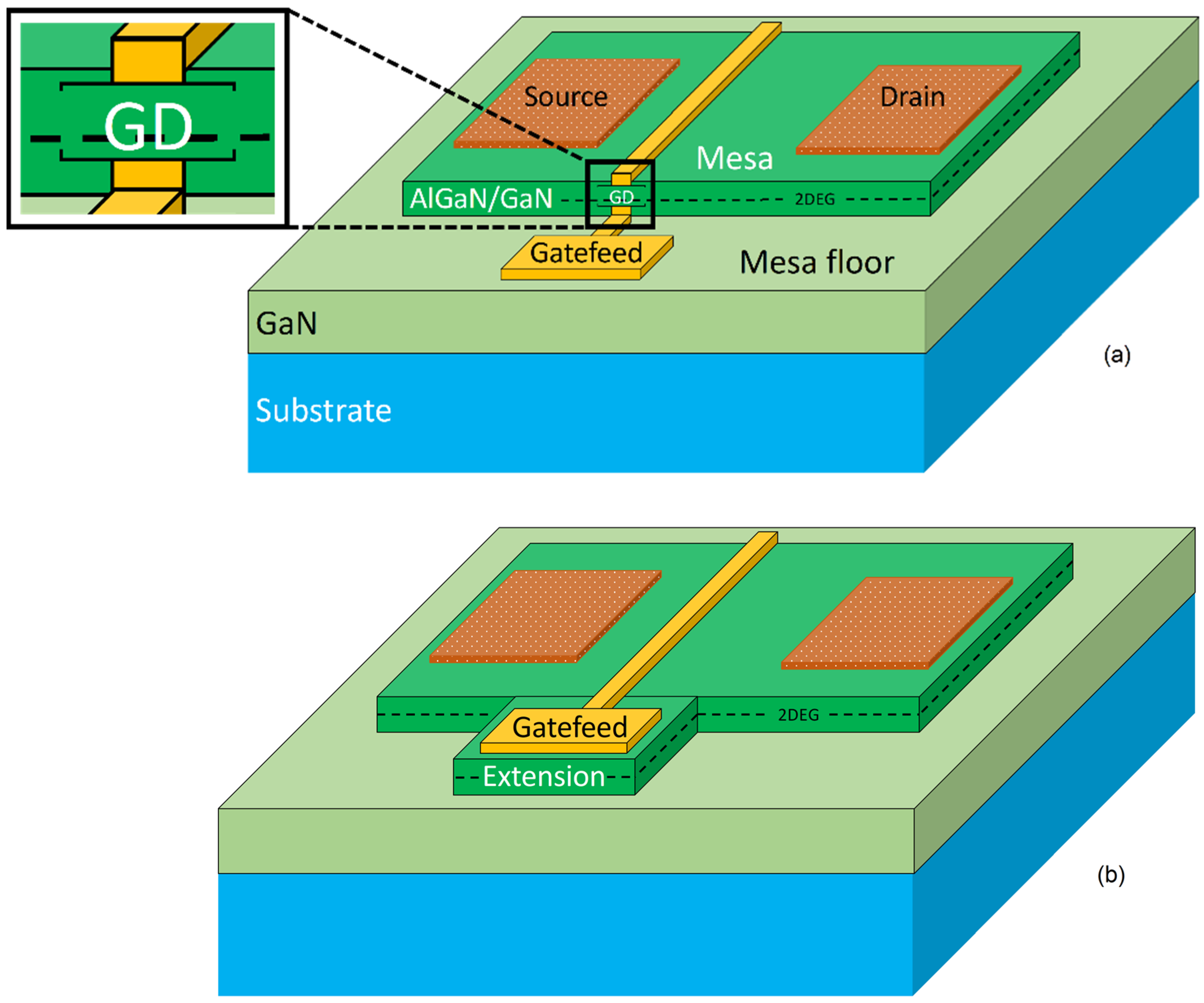
Gallium nitride (GaN) is one of the most attractive semiconductors due to its inherent characteristics, such as electron mobility and saturation velocity, enabling the feasibility of high-power devices at microwave frequency with a considerably enhanced power density [1,2,3,4,5,6]. Currently, GaN-based HEMT devices fabrication includes a device isolation step performed by a conventional mesa etch or ion implantation to suppress the two-dimensional-electron-gas (2DEG) and electrically insulate devices. Although a three-dimensional (3D)-structure device is obtained due to physical removal of material, the former (mesa) is widely used for cost purposes. However, the introduction of a nonplanar structure in HEMTs results in a high gate leakage current, which degrades noise performance in RF amplifiers and can drive the device into breakdown prematurely [7,8]. This is because of the presence of a mesa sidewall in the conventional mesa-isolation process, the metal gate and/or the passivation layer come into contact with the 2DEG of the AlGaN/GaN HEMT structure, resulting in higher gate leakage current and non-uniformity in buffer breakdown voltage with passivation layer [9,10]. Additionally, there is possible metallic discontinuity of the gate at the mesa edge, especially at a small gate length Lg ≤ 1.0 µm as shown in Figure 1a. Besides, in a mesa isolation, etch depth is critical for reproducible, optimized device and circuit performance. Under-etching causes current leakage and poor pinch-off of HEMTs, affects bias levels in circuits, and alters transmission line impedances [11]. In contrast, ion implantation isolation preserves the planar structure of the device but at a considerably higher cost [12]. Additionally, near-surface ion implants greatly degraded the resistivity of the damaged GaN. The considerable decrease in resistivity of the implant-damaged GaN after annealing at relatively low temperatures would most likely limit the use of ion implantation for lower temperature applications [13,14]. Other researchers have examined alternative methods, such as thermal oxidization, as reported in [15,16]. However, this process can affect the 2DEG beneath the actual device due to high temperature sample exposure for long durations, up to 900 °C and 30 min, respectively. Finally, as a technique to mitigate the metallic gate-discontinuity and leakage complications, air bridging the gate across to the bond pads has also been investigated as reported in [17,18,19]. Nevertheless, the process is complex [12] and can reduce device reproducibility and yield.
In this paper, a novel approach is provided to overcome the existing tradeoff between cost and 3D-structure disadvantages. A miniature extension from the mesa is employed to accommodate the gatefeed, which is the interconnect between the gate itself and the measurement bond pads (or transmission lines in integrated circuits). This, as a result, ensures a gate continuity, integrity, and reduces the gate leakage current since the critical section of the gate metal is positioned planarly on the mesa/extension in its entirety as illustrated in Figure 1b. Therefore, a direct contact between the gate and the 2DEG is avoided. Moreover, the bond pads or transmission lines are large features with a Si3N4 passivation underneath, hence a metal discontinuity and a direct 2DEG contact, respectively, are implausible to be present. The fabricated devices have the following dimensions: a device width of 125 µm, a gate foot length of 1.0 µm, a gate head of 1.5 µm, a total source-drain separation of 5 µm, a 1.5 µm of gate-source spacing and a 2.5 µm gate-drain distance. All the devices in this work have two gate fingers.
2. Materials and Methods
2.1. Material Growth
The devices in this work were fabricated using AlGaN/AlN/GaN epitaxy grown on 6-inch p-type low resistivity silicon (LR-Si) substrate by metal organic chemical vapor deposition (MOCVD). The GaN epilayer consists of a 200 nm AlN nucleation and a 750 nm graded buffer of AlGaN, both of which are applied to accommodate the lattice mismatch between the LR-Si substrate and GaN epitaxy to reduce the bow condition on the surface. Subsequently, a 1400 nm Fe-doped GaN graded buffer and channel, a 1 nm AlN spacer, a 25 nm AlxGa1-xN barrier with Al composition (x) of 25% and finally capped with a 2 nm GaN to further manage the tensile strain on the barrier. The wafer from end-to-end is crack free with a maximum concave bow of only 20 µm, which was acquired after exposure to a high temperature around 1050 °C, during growth, followed by a cooling process.
2.2. Device Process
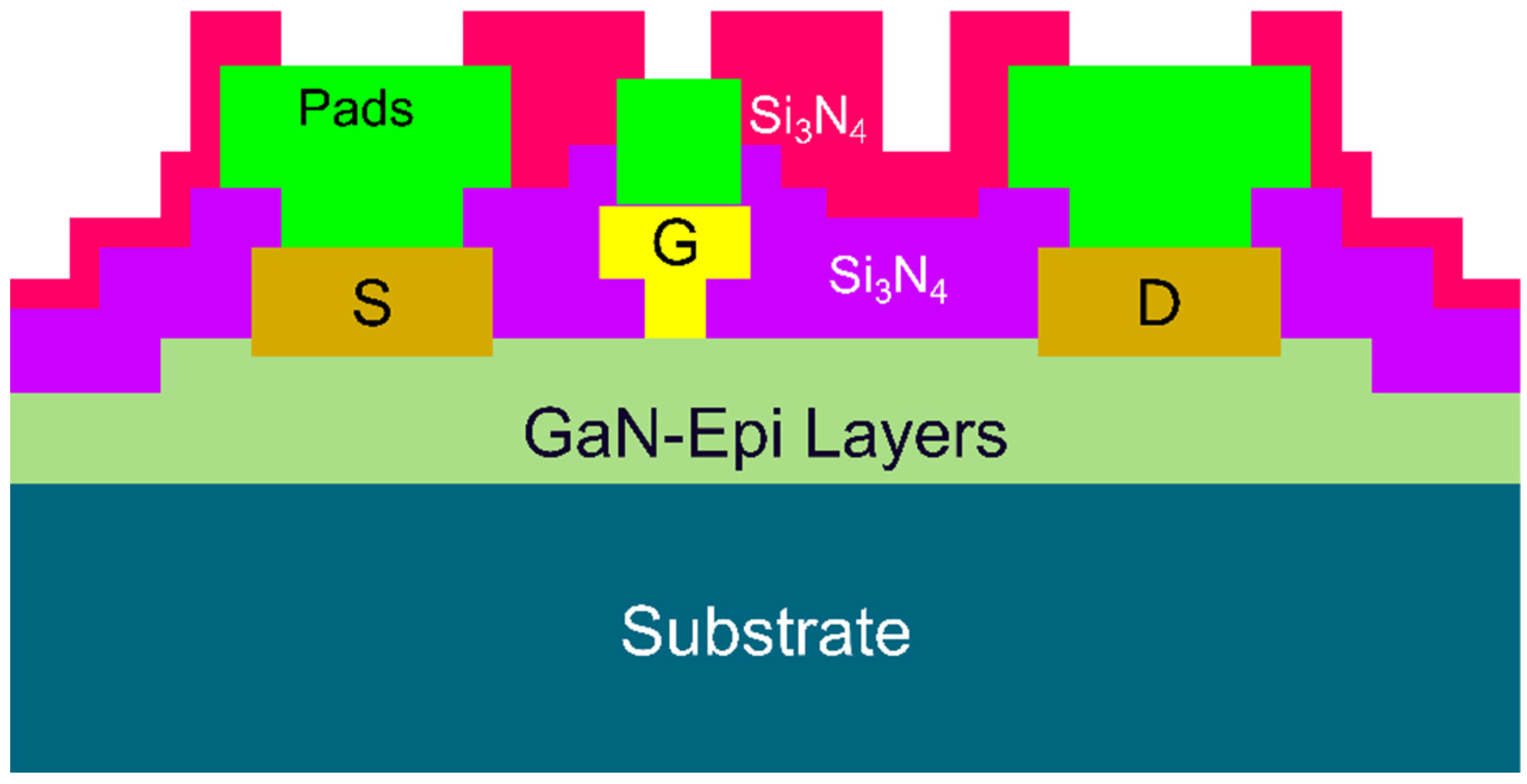
In this work, all levels of device definition were realized using photolithography. The process commences with the fabrication of alignment markers. After that, the ohmic contacts (source/drain) were realized using the standard AlGaN/GaN HEMT metal scheme (Ti/Al/Ni/Au) and annealed at 790 °C for 30 s in N2 atmosphere. Next, mesa isolation at a depth of 200 nm was applied to remove the active layers between devices using a chlorine-based mixture of gases in an Inductively Coupled Plasma-Reactive Ion Etching (ICP-RIE) tool. After that, a 100 nm S3iN4 a blanket passivation was deposited by method of plasma enhanced chemical vapor deposition (PECVD) at 300 °C. The purpose of the first passivation layer is to suppress surface leakage and trappings, which can lead to a device unreliability. Then, gate footprints were realized using a low-damage SF6/N2 plasma etch to remove the Si3N4 passivation from underneath the gate foot. The metal (Ni/Au 20/200 nm) of the gate and its feed were then evaporated to form the Schottky contact of the device. Finally, after a second S3iN4 blanket passivation and openings etch, the bond pad metal was deposited for measurement using Ti/Au metal-stack with a metal thickness of 50/700 nm. The second passivation layer is applied only to protect the devices from oxidation and corrosion, which can help to extend the lifetime of the devices. The cross-section of the fabricated devices is given in Figure 2.
2.3. Proposed Devices Design
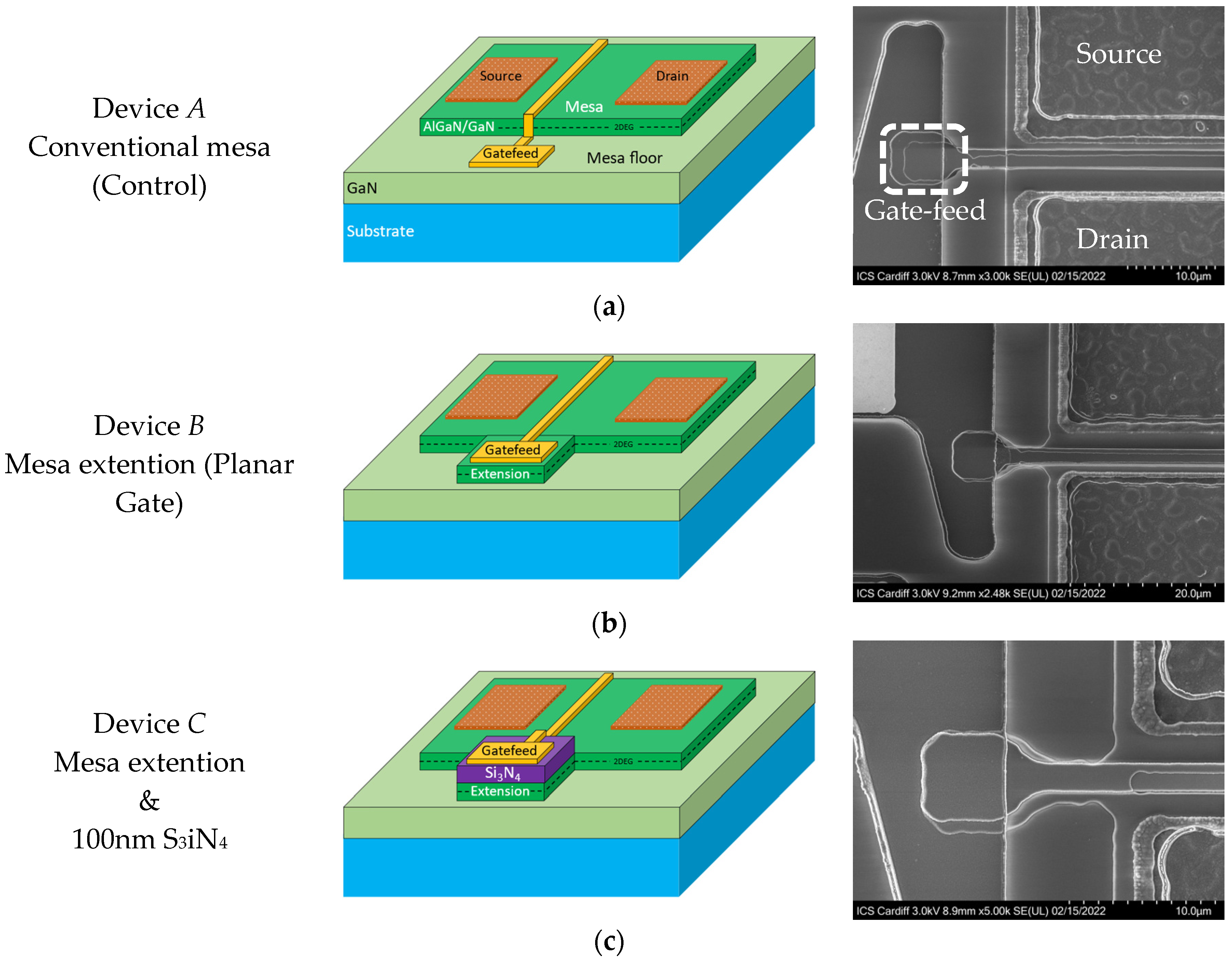
In this work, three device structures are fabricated as shown in Figure 3. The first one (device A) is the conventional HEMT, which has its gate-feed directly on the GaN semiconductor after etching the Si3N4 passivation. Device A is the control device to which the proposed devices results are compared to. The proposed device is fabricated into two different structures with respect to the location of the gate-feed. The first and the primary proposed device has its gate-feed directly on the proposed miniature mesa extension and the second one the gate-feed is elevated above the extension by a 100 nm of Si3N4, annotated by device B and C, respectively. It is worth noting that the footprint of the gate-feed of device B is situated directly on an active layer (i.e., the mesa extension) and it is wide in size (3.5 µm wider than the gate footprint). This ultimately results in a lower resistance path at the gate-feed of device B. Therefore, the fabrication of device C is necessary to suppress the lower resistance access point, obtained in device B, by adding an insulation layer below the gate-feed. Although this results in a non-planar device, nevertheless the gate has no direct contact with the 2DEG channel. This will enable for a clearer observation and characterization of the active layer influence on the performance of device B.
The mesa extension, as shown in Figure 3, is designed to accommodate the gate-feed. The length of the mesa extension is 13 µm from the actual device-mesa and the width is designed to be larger than the gate and the gate-feed by 0.5 µm on all sides to avoid any potential misalignment may be arising from the photolithography. Both proposed structures are compatible with the conventional GaN HEMTs process, therefore realizable without any additional fabrication requirements.
3. Results and Discussion
3.1. DC and RF Performance
On-wafer DC and RF measurements were performed using an Agilent semiconductor parameter analyzer (B1500A, Agilent Technologies, Santa Clara, CA, USA) and a microwave network analyzer (N5227A, Keysight Technologies, Santa Rosa, CA, USA), respectively. The latter was calibrated from 100 MHz up to 50 GHz with an off-wafer impedance standard substrate (ISS) calibration kit for a 100 µm pitch RF-probe by utilizing a Short-Open-Load-Through (SOLT) calibration procedure at a small signal RF excitation (−20 dBm).
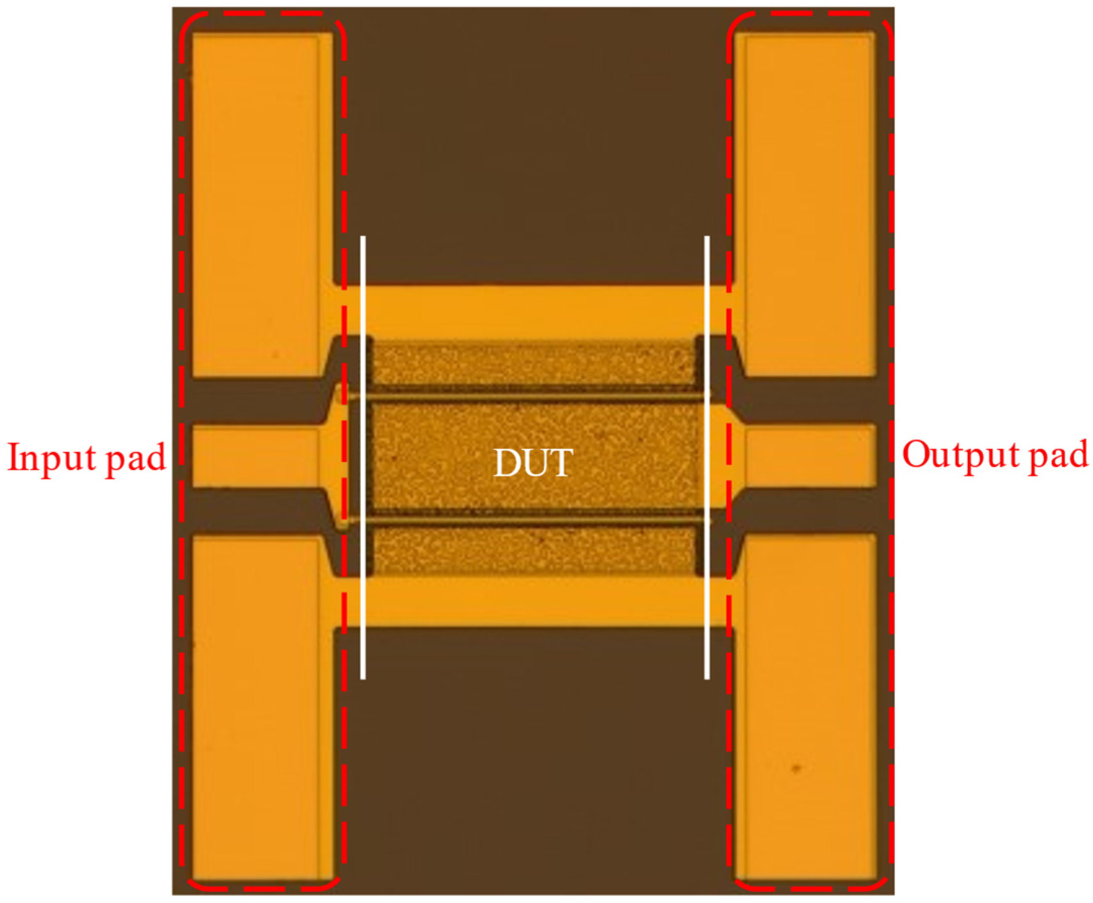
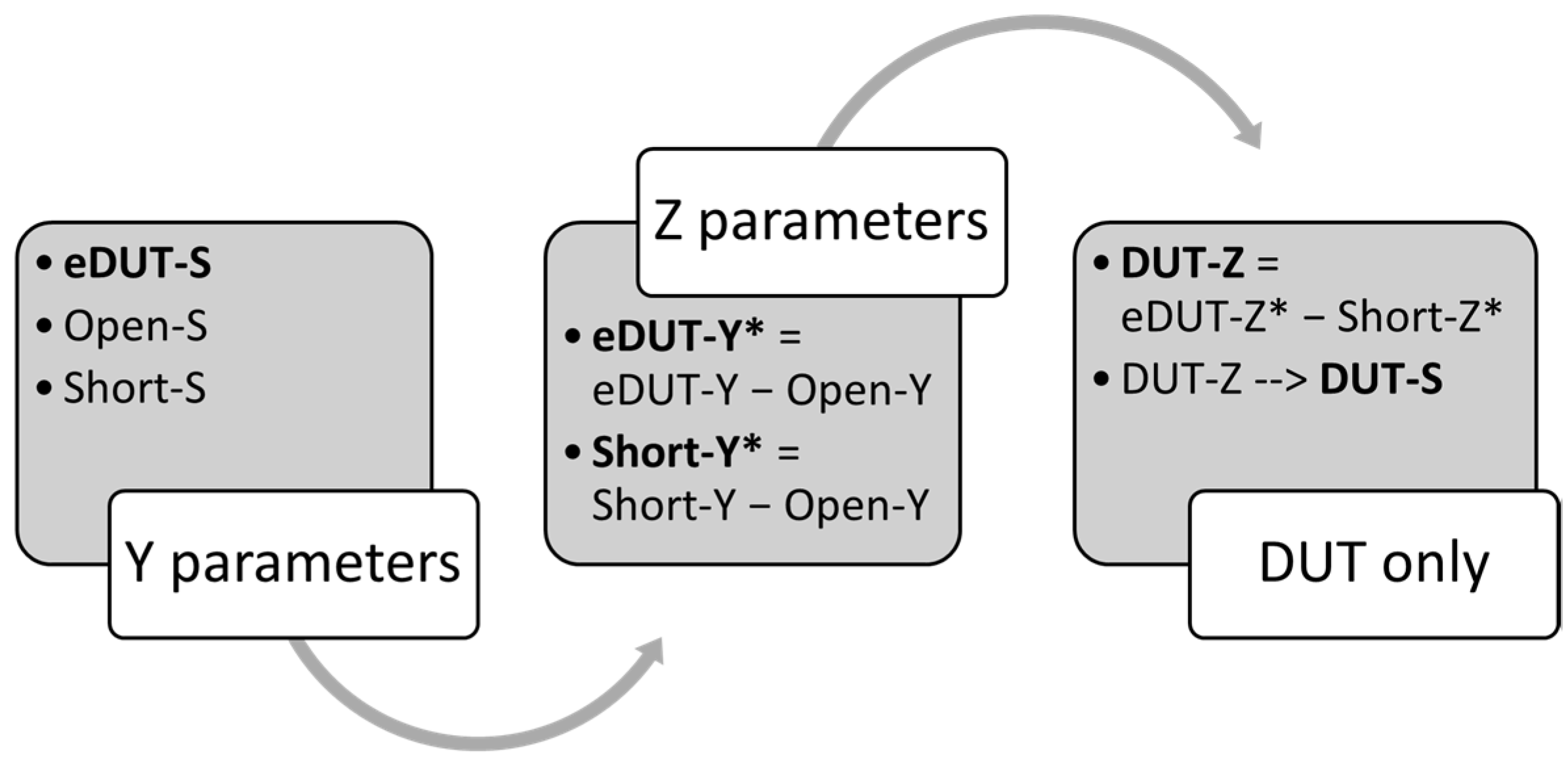
To accurately assess the fabricated device at high frequency, a de-embedding process is executed to remove the pads parasitic impedances from the device under test (DUT) as shown in Figure 4. The de-embedding method begins with three measurements, the embedded-DUT (eDUT), an open and short “dummy” structures of the pads without the device. The de-embedding technique is carried out directly on the measurement system using a customized routine in Keysight PathWave Device Modeling software (IC-CAP 2020, Keysight Technologies, Santa Rosa, CA, USA), in which an algorithm is coded to mathematically remove the measurement bond-pads effects (the open and short) from the measured data.
All RF measurements are initially collected in a two-port S-parameters format. This is followed by conversion to Y-parameters for the three measurements. The Y-parameters of the open fixture is then subtracted from the eDUT and the short fixture measurements. Finally, the partial de-embedded data of eDUT-Y* and de-embedded short fixture (Short-Y*) are converted to Z-parameters, forming eDUT-Z* and Short-Z* respectively. The latter is then subtracted from the former resulting in a fully de-embedded data which is then converted back to S-parameters format (DUT-Z → DUT-S) for further mathematical manipulation. Figure 5 summarizes the process flow and the algorithm for the device de-embedding methodology utilized in this work.
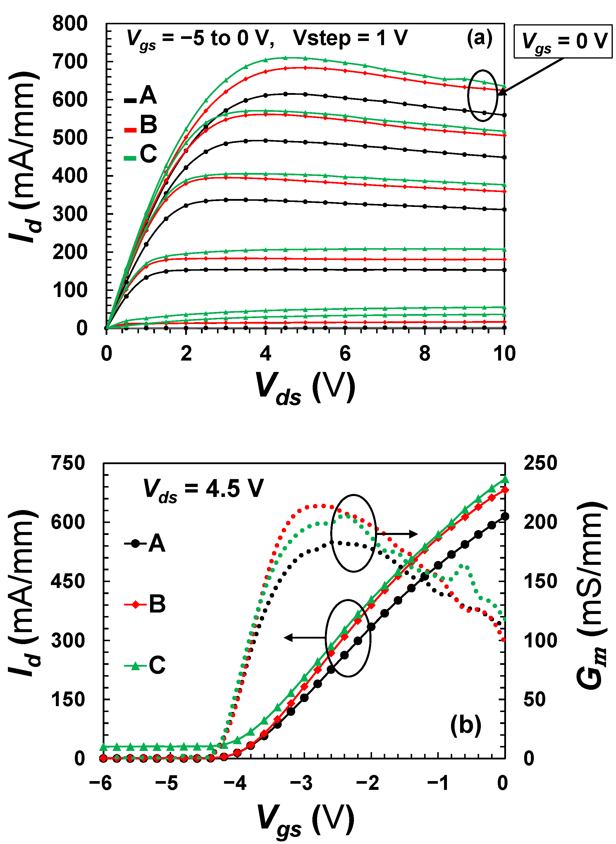
An assessment of IV characteristics on all three devices was performed to validate the influence of mesa extension on device performance in terms of output current, as shown in Figure 6a. The maximum drain current, IDSS, of the three devices is 692, 772 and 813 mA/mm for device A, B and C, respectively, obtained at Vds = 4.5 V. The increase of maximum current in the proposed devices is stemming from the reduction in the On-resistance (RON) from 3.57 Ω⋅mm for device A to 3.23 and 3.05 Ω⋅mm for device B and C respectively. Further, a well pinch-off behavior is found in all devices at −4.2 V as depicted in Figure 6b. However, in Figure 6b also, a drain leakage is observed in device C evidenced by the drain current not approaching the zero point of the y-axis as the other devices. This drain leakage was observed in all measured C-type devices across the entire wafer. This is usually ascribed to traps in AlGaN/GaN HEMTs associated with electron injection from the gate and trapping either inside the AlGaN layer or at the surface close to the gate [20]. Nonetheless, since device A and B, which were fabricated on the same wafer, did not exhibit such issue with drain leakage, the aforementioned traps in the materials are unlikely to be the cause of the drain leakage in device C. Therefore, given that device C is the only device configuration with an insulation layer (100 nm of Si3N4) below its gate-feed, this can be considered as the leading trigger for the device drain current leakage (further analysis is given next in Section 3.2).
Additionally, at Vds = 4.5 V and Vgs = −3 V, a maximum DC transconductance (Gm) was obtained for the three devices. However, the proposed devices exhibited an increase of Gm by almost 20% from 177 to 200 mS/mm, which can be attributed to the increase of the gate width (Wg) by a total of 26 µm (2-finger × 13 µm ≈ 20% total width increase) due to the mesa extension as predicted from the following formula [21,22]:
where εbarrier is barrier layer dielectric constant, vsat is the saturation velocity, dbarrier is the barrier layer thickness, and Δd is the effective distance of the 2DEG from the heterointerface.
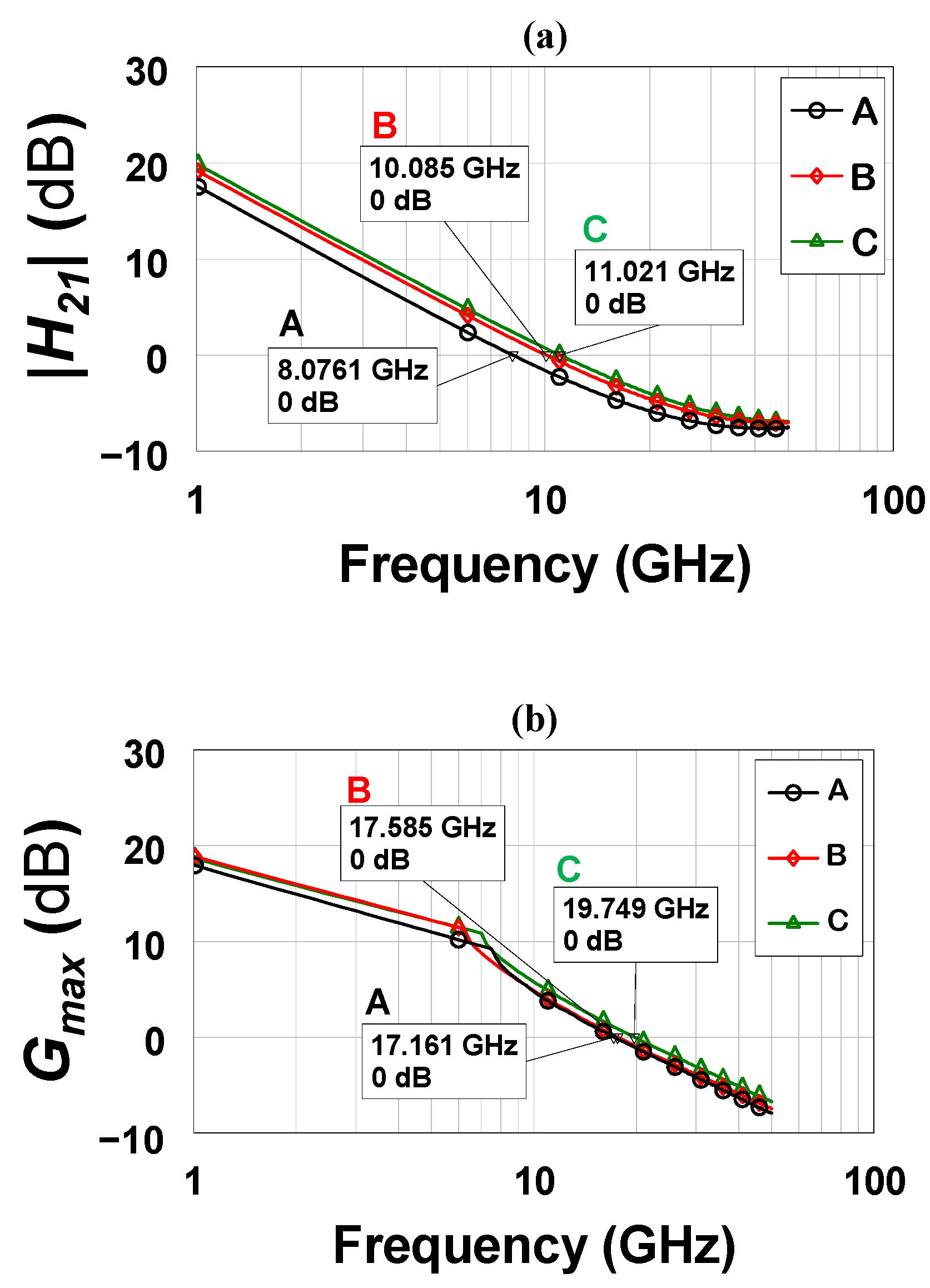
A comparison of RF performance was conducted to substantiate the impact of mesa extension on device performance in terms of device cutoff (ƒT) and maximum oscillation (ƒmax) frequencies, which can be evaluated using Equations (2) and (3), respectively. Figure 7 shows a rise in ƒT and ƒmax as the gatefeed location is altered triggered by the increase in RF transconductance (gm) and/or the decrease in gate-drain/source capacitances [23] extracted from a small signal model.
where Cgs is the gate-source capacitance, Cgd is the gate-drain capacitance, Rg is the gate resistance, Rin is the input resistance and Rds is the output resistance.
Device B demonstrated the highest gm (108 mS) with an increase of 80% in comparison with the control device (device A) with only 60 mS of gm. Device C, on the other hand, showed a 25% increase in gm. Even though the proposed device exhibited the highest gm, a clear DC-to-RF dispersion is present manifested by the variations between DC and RF transconductances, i.e., Gm and gm, respectively. This was the case for all of the fabricated devise across the entire wafer. This could be attributed to the quality of the passivation utilized in this work. GaN devices, in general, have been demonstrated to be extremely sensitive to various surface passivation and preparation procedures, indicating that trapped surface charge plays a substantial role in the dispersion [24,25].
In a field effect transistor (FET), the source of fringing capacitance between the electrodes are due to the electric field’s lines occurring between them. This electric field is present in the air (at the surface) and more strongly within the semiconductor, assuming there is no surface passivation, due to a higher dielectric constant (εr ≈ 8.9 for GaN material). However, stronger electric field at the surface can occur if a passivation layer is deposited on the device leading to an increase of the overall fringing capacitance. For example, a 20% increase in fringing capacitance is obtained using a 30 nm of Al2O3 passivation as reported in [26]. In addition, knowing that the fringing capacitance (Cf) is inversely proportional to the distance (d) between the electrodes as given in Equation (4).
where A is the area of plates (the metallic surface of electrodes), εo is the permittivity of free space and εr is the relative permittivity of the material. Although, the inclusion of the mesa extension increases the distance between the gate-feed and the source/drain contacts from the GaN semiconductor side (by 200 nm), the distance at the surface is in fact reduced since they are on the same level plane with a 100 nm Si3N4 dielectric between them. This explains the increase in fringing capacitance acquired in device B. Nevertheless, device B exhibited a slight improvement in RF performance, in comparison with the control device, merely due to the improvement in gm. Device C, on the hand, showed the optimum enhancement in RF performance with 35% and 15% increase in ƒT and ƒmax, respectively. This is primarily the result of the reduction in fringing capacitance due to the presence of Si3N4 below the gate-feed. This further increases the distance between the gate-feed and the source/drain electrodes resulting in a lower electric coupling and thereby a lower capacitance at the semiconductor and at the surface simultaneously. A detailed comparative study between mesa and ion-implantation isolation with respect to RF performance is reported in [27]. The study shows a reduction in the gate fringing capacitance by 5.6% and an increase in gm by more than 11% for ion-implanted device in comparison to a mesa etched one. These attainments resulted in an average increase of 17% in ƒT. The authors attributed the improvement obtained by ion-implantation isolation in part to defects generated at the ICP-etched mesa edge and/or even on the mesa floor surface due to ion bombardment during the dry etch process [27,28].
Summary of DC and RF parameters for the fabricated devices are included in Table 1. No compromise in performance is observed for the fabricated devices. This manifests that the proposed mesa extension is not presenting any deterioration to the parameters of the devices. In fact, the proposed devices can offer a higher power density in comparison with the conventional one. Almost 10–14% increase in power density is obtained by the proposed devices. This is equal in percentage to the amount of reduction achieved in Ron.
3.2. Gate and Drain Leakage Currents
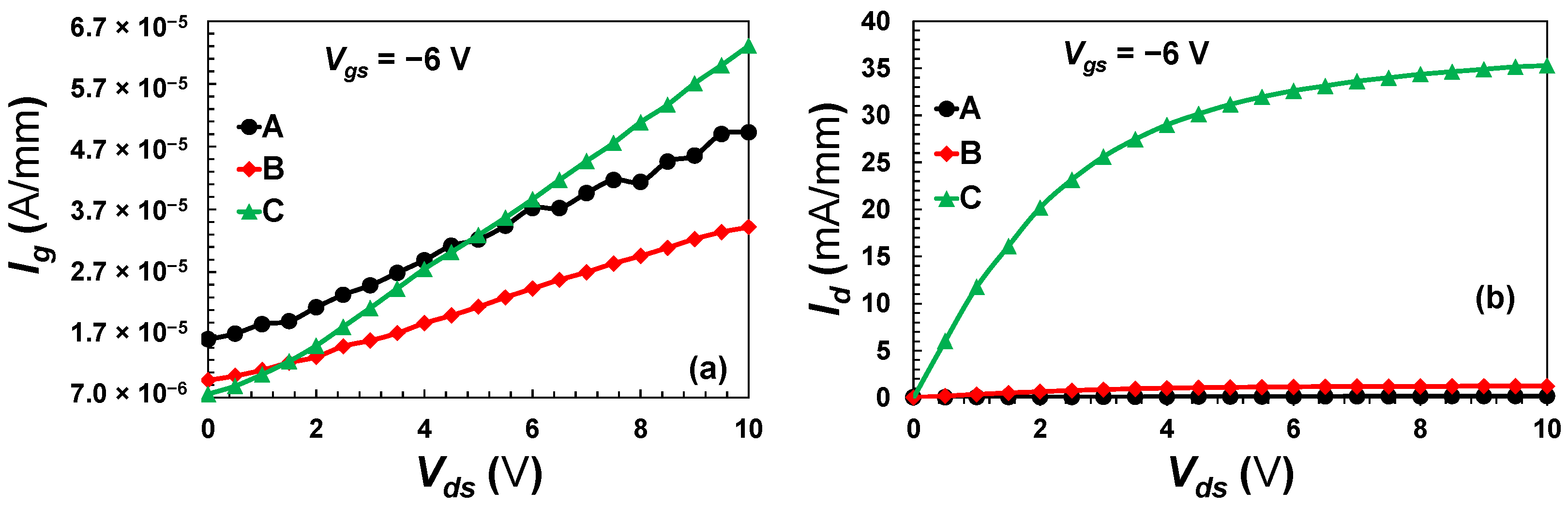
An evaluation of gate and drain currents on the devices was performed to validate the effect of mesa extension on device performance in terms of leakage, as demonstrated in Figure 8. The off-state gate leakage current of all devices is shown in Figure 8a with a drain voltage sweep from 0 to 10 V and a gate voltage of −6 V. Across the entire drain bias, device A exhibited an order of magnitude larger gate leakage currents than device B. The proposed planar gate device, with mesa extension, revealed lower gate leakage currents as expected compared to the conventional one, which is comparable to the decrease obtained by 131Xe+ ion-implantation as given in [29]. This is due to the gate in the conventional device being in a direct contact with the 2DEG channel [30,31] while the gate in the planar device has the AlGaN barrier acting as an insulator between the gate and the 2DEG. However, device C demonstrated a low gate leakage at lower drain voltages and vice versa at higher biasing with an order of magnitude of leakage between the minimum and maximum Vds. This is attributed to the device’s poor linearity [31] evidenced by the irregular shape of the Gm displayed by device C as shown in Figure 6b. Additionally, due to the use of PECVD in the formation of Si3N4, a hot hole injection and trapping is present at the insulator/semiconductor interface [32]. Takatani et al. further explain that the hot holes produced by impact ionization at the gate’s drain end are injected and trapped at the insulator/semiconductor interface between the gate and the drain, thus increasing the electric field at the gate-edge. This is attributed to a couple major drawbacks of the PECVD method: (1) generated films contain large concentrations of bound hydrogens, and (2) surface damage can be induced by the bombardment of high-energy ions, resulting in a high density of interface states [33].
Subsequently, with the same bias conditions, the off-state drain leakage current of the fabricated devices is also presented in Figure 8b. Device A, B and C exhibited 0.19, 1.24 and 35.3 mA/mm of drain leakage, respectively, at a drain voltage of 10 V. This is primarily due to the degraded gate controllability over the drain-source channel as the distance between the gate edges and the 2DEG is enhanced [34,35].
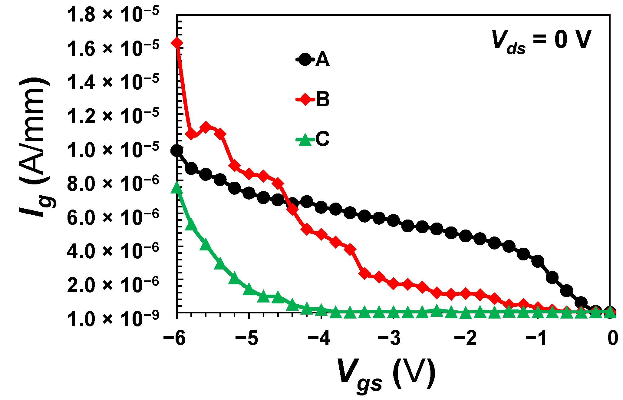
Finally, the devices were swept at the gate terminal from −6 to 0 V without drain bias, i.e., Vds = 0 V. Both proposed devices (B and C) exhibited the minimum gate leakage particularly between −4.5 and −0.5 V of a gate bias, whereas the control device demonstrated an order of magnitude higher gate leakage at the same bias level as depicted in Figure 9. This is mainly due to the direct contact between the gate electrode and the 2DEG as in device A. Moreover, due to the absence of a drain bias, device C showed an optimum suppression of gate leakage in comparison with the other devices. However, the leakage is considerably enhanced in device C when a drain bias is applied caused by the hot hole injection and the trapping as aforementioned.
4. Conclusions
In this work, a newly developed structure is proposed to overcome mesa etch drawbacks, such as mesa sidewall profile, common gate discontinuity, and gate leakage originated from a gate direct contact with 2DEG. The proposed structure requires a miniature extension of the mesa to deposit the gatefeed, thereby ensuring a fully planar gate formation. This, as a result, reduces the etching complexity and circumvents the direct contact between the gate and the 2DEG. With more than an order of magnitude of gate leakage suppression, the proposed device also showed a better DC and RF performance than the conventional device. Further investigation, however, is necessary to fully understand the rise of the drain off-state current of the planar device and to find a method to enhance the gate controllability of the device.
Author Contributions
Conceptualization, methodology, device engineering, fabrication, characterization, results analysis, and discussion, writing original draft, M.A.; Supervision, review, and editing, K.E. All authors have read and agreed to the published version of the manuscript.
Funding
The Open Access (OA) charges of this work has been funded from the Cardiff University Institutional OA Fund, Ref. number: 2022-OA-0821.
Data Availability Statement
The data presented within this paper is available on a reasonable request from the first author.
Acknowledgments
The first author would like to thank King Saud University, Saudi Arabia, for the financial support during his postgraduate study at Cardiff University, UK. The authors would also like to thank the School of Engineering, Cardiff University, for supporting this research work by funding the APC towards publishing this paper.
Conflicts of Interest
The authors declare no conflict of interest.
References
- Palacios, T.; Shen, L.; Keller, S.; Chakraborty, A.; Heikman, S.; Buttari, D.; DenBaars, S.P.; Mishra, U.K. Demonstration of a GaN-spacer high electron mobility transistor with low alloy scattering. Phys. Status Solidi 2005, 202, 837–840. [Google Scholar] [CrossRef]
- Brown, J.D.; Borges, R.; Piner, E.; Vescan, A.; Singhal, S.; Therrien, R. AlGaN/GaN HFETs fabricated on 100-mm GaN on silicon (111) substrates. Solid State Electron. 2002, 46, 1535–1539. [Google Scholar] [CrossRef]
- Chung, J.W.; Hoke, W.E.; Chumbes, E.M.; Palacios, T. AlGaN/GaN HEMT with 300-GHz fmax. IEEE Electron Device Lett. 2010, 31, 195–197. [Google Scholar] [CrossRef]
- Arulkumaran, S.; Ng, G.I.; Liu, Z.H.; Lee, C.H. High temperature power performance of AlGaN∕GaN high-electron-mobility transistors on high-resistivity silicon. Appl. Phys. Lett. 2007, 91, 083516. [Google Scholar] [CrossRef]
- Leone, S.; Benkhelifa, F.; Kirste, L.; Manz, C.; Quay, R.; Ambacher, O. Epitaxial growth optimization of AlGaN/GaN high electron mobility transistor structures on 3C-SiC/Si. J. Appl. Phys. 2019, 125, 235701. [Google Scholar] [CrossRef]
- Eblabla, A.; Li, X.; Alathbah, M.; Wu, Z.; Lees, J.; Elgaid, K. Multi-Channel AlGaN/GaN Lateral Schottky Barrier Diodes on Low-Resistivity Silicon for Sub-THz Integrated Circuits Applications. IEEE Electron Device Lett. 2019, 40, 878–880. [Google Scholar] [CrossRef] [Green Version]
- Sanabria, C.; Chakraborty, A.; Xu, H.; Rodwell, M.J.; Mishra, U.K.; York, R.A. The effect of gate leakage on the noise figure of AlGaN/GaN HEMTs. IEEE Electron Device Lett. 2006, 27, 19–21. [Google Scholar] [CrossRef]
- Pearton, S.J.; Shul, R.J.; Ren, F. A review of dry etching of GaN and related materials. MRS Internet J. Nitride Semicond. Res. 2000, 5, e11. [Google Scholar] [CrossRef] [Green Version]
- Arulkumaran, S.; Ranjan, K.; Ng, G.I.; Kennedy, J.; Murmu, P.P.; Bhat, T.N.; Tripathy, S. Thermally stable device isolation by inert gas heavy ion implantation in AlGaN/GaN HEMTs on Si. J. Vac. Sci. Technol. B Nanotechnol. Microelectron. Mater. Process. Meas. Phenom. 2016, 34, 042203. [Google Scholar] [CrossRef]
- Mojaver, H.R.; Valizadeh, P. Reverse Gate-Current of AlGaN/GaN HFETs: Evidence of Leakage at Mesa Sidewalls. IEEE Trans. Electron Devices 2016, 63, 1444–1449. [Google Scholar] [CrossRef]
- Elgaid, K.I. A Ka-Band GaAs MESFET Monolithic Downconverter; University of Glasgow: Glasgow, Scotland, 1998. [Google Scholar]
- Bahl, S.R.; Leary, M.H.; del Alamo, J.A.; Bahl, S.R.; del Alamo, J.A. Mesa-Sidewall Gate Leakage in InAlAs/InGaAs Heterostructure Field-Effect Transistors. IEEE Trans. Electron Devices 1992, 39, 2037–2043. [Google Scholar] [CrossRef] [Green Version]
- Binari, S.C.; Dietrich, H.B.; Kelner, G.; Rowland, L.B.; Doverspike, K.; Wickenden, D.K. H, He, and N implant isolation of n-type GaN. J. Appl. Phys. 1998, 78, 3008. [Google Scholar] [CrossRef]
- Johra, F.T.; Jung, W.G. Effect of light-ions implantation on resistivity of GaN thin film. Electron. Mater. Lett. 2014, 10, 699–702. [Google Scholar] [CrossRef]
- Roccaforte, F.; Giannazzo, F.; Iucolano, F.; Bongiorno, C.; Raineri, V. Electrical behavior of AlGaN/GaN heterostuctures upon high-temperature selective oxidation. J. Appl. Phys. 2009, 106, 023703. [Google Scholar] [CrossRef]
- Masato, H.; Ikeda, Y.; Matsuno, T.; Inoue, K.; Nishii, K. Novel high drain breakdown voltage AlGaN/GaN HFETs using selective thermal oxidation process. In Proceedings of the International Electron Devices Meeting 2000. Technical Digest. IEDM (Cat. No.00CH37138), San Francisco, CA, USA, 10–13 December 2000; pp. 377–380. [Google Scholar]
- Fathimulla, A.; Abrahams, J.; Loughran, T.; Hier, H. High-Performance InAlAs/InGaAs HEMT’s and MESFET’s. IEEE Electron Device Lett. 1988, 9, 328–330. [Google Scholar] [CrossRef]
- Newson, D.J.; Merrett, R.P.; Ridley, B.K. Control of gate leakage in InAIAs/InGaAs Hemts. Electron. Lett. 1991, 27, 1592–1593. [Google Scholar] [CrossRef]
- Boos, J.B.; Kruppa, W. InAIAs/InGaAs/InP HEMTs with high breakdown voltages using double-recess gate process. Electron. Lett. 1991, 27, 1909–1910. [Google Scholar] [CrossRef]
- Joh, J.; del Alamo, J.A. A Current-Transient Methodology for Trap Analysis for GaN High Electron Mobility Transistors. IEEE Trans. Electron Devices 2011, 58, 132–140. [Google Scholar] [CrossRef] [Green Version]
- AlN/GaN MOS-HEMTs Technology—Enlighten: Theses. Available online: https://theses.gla.ac.uk/3356/ (accessed on 5 April 2022).
- Hou, B.; Yang, L.; Mi, M.; Zhang, M.; Yi, C.; Wu, M.; Zhu, Q.; Lu, Y.; Zhu, J.; Zhou, X.; et al. High linearity and high power performance with barrier layer of sandwich structure and Al0.05GaN back barrier for X-band application. J. Phys. D Appl. Phys. 2020, 53, 145102. [Google Scholar] [CrossRef]
- Min, S.R.; Cho, M.S.; Lee, S.H.; Park, J.; An, H.D.; Kim, G.U.; Yoon, Y.J.; Seo, J.H.; Jang, J.W.; Bae, J.H.; et al. Analysis for DC and RF Characteristics Recessed-Gate GaN MOSFET Using Stacked TiO2/Si3N4 Dual-Layer Insulator. Materials 2022, 15, 819. [Google Scholar] [CrossRef]
- Tan, W.S.; Houston, P.A.; Parbrook, J.; Hill, G.; Airey, R.J. Comparison of different surface passivation dielectrics in AlGaN/GaN heterostructure field-effect transistors. J. Phys. D Appl. Phys. 2002, 35, 595–598. [Google Scholar] [CrossRef]
- Roff, C.; Benedikt, J.; Tasker, P.J.; Wallis, D.J.; Hilton, K.P.; Maclean, J.O.; Hayes, D.G.; Uren, M.J.; Martin, T. Analysis of DC-RF dispersion in AlGaN/GaN HFETs using RF waveform engineering. IEEE Trans. Electron Devices 2009, 56, 13–19. [Google Scholar] [CrossRef] [Green Version]
- Lee, D.S.; Laboutin, O.; Cao, Y.; Johnson, W.; Beam, E.; Ketterson, A.; Schuette, M.; Saunier, P.; Palacios, T. Impact of Al2O3 passivation thickness in highly scaled GaN HEMTs. IEEE Electron Device Lett. 2012, 33, 976–978. [Google Scholar] [CrossRef]
- Sun, H.; Alt, A.R.; Tirelli, S.; Marti, D.; Benedickter, H.; Piner, E.; Bolognesi, C.R. Nanometric AlGaN/GaN HEMT performance with implant or mesa isolation. IEEE Electron Device Lett. 2011, 32, 1056–1058. [Google Scholar] [CrossRef]
- Shul, R.J.; Zhang, L.; Baca, A.G.; Willison, C.G.; Han, J.; Pearton, S.; Lee, K.P.; Ren, F. Inductively Coupled High-Density Plasma-Induced Etch Damage of GaN MESFETs. MRS Online Proc. Libr. 2000, 622, T7.5.1. [Google Scholar] [CrossRef]
- Li, Y.; Ng, G.I.; Arulkumaran, S.; Liu, Z.H.; Ranjan, K.; Ang, K.S.; Murmu, P.P.; Kennedy, J. Improved planar device isolation in AlGaN/GaN HEMTs on Si by ultra-heavy 131Xe+ implantation. Phys. Status Solidi Appl. Mater. Sci. 2017, 214, 1600794. [Google Scholar] [CrossRef]
- Shiu, J.-Y.; Huang, J.-C.; Desmaris, V.; Chang, C.-T.; Lu, C.-Y.; Kumakura, K.; Makimoto, T.; Zirath, H.; Rorsman, N.; Chang, E.Y. Oxygen ion implantation isolation planar process for AlGaN/GaN HEMTs. IEEE Electron Device Lett. 2007, 28, 476–478. [Google Scholar] [CrossRef] [Green Version]
- Chiu, H.-C.; Chen, C.-H.; Kao, H.-L.; Chien, F.-T.; Weng, P.-K.; Gau, Y.-T.; Chuang, H.-W. Sidewall defects of AlGaN/GaN HEMTs evaluated by low frequency noise analysis. Microelectron. Reliab. 2013, 53, 1897–1900. [Google Scholar] [CrossRef]
- Takatani, S.; Matsumoto, H.; Shigeta, J.; Ohshika, K.; Yamashita, T.; Fukui, M. Generation mechanism of gate leakage current due to reverse-voltage stress in i-AlGaAs/n-GaAs HIGFET’s. IEEE Trans. Electron Devices 1998, 45, 14–20. [Google Scholar] [CrossRef]
- Ohta, H.; Nagashima, A.; Ito, M.; Hori, M.; Goto, T. Formation of silicon nitride gate dielectric films at 300 °C employing radical chemical vapor deposition. J. Vac. Sci. Technol. B Microelectron. Nanom. Struct. Process. Meas. Phenom. 2000, 18, 2486. [Google Scholar] [CrossRef]
- Hwang, I.T.; Jang, K.W.; Kim, H.J.; Lee, S.H.; Lim, J.W.; Yang, J.M.; Kwon, H.S.; Kim, H.S. Analysis of DC characteristics in GaN-based metal-insulator-semiconductor high electron mobility transistor with variation of gate dielectric layer composition by considering self-heating effect. Appl. Sci. 2019, 9, 3610. [Google Scholar] [CrossRef]
- Chu, R.; Shen, L.; Fichtenbaum, N.; Brown, D.; Keller, S.; Mishra, U.K. Plasma treatment for leakage reduction in AlGaN/GaN and GaN Schottky contacts. IEEE Electron Device Lett. 2008, 29, 297–299. [Google Scholar]
Figure 1.
Conventional gallium nitride (GaN)-based high electron mobility transistor (HEMT) device with its gatefeed on mesa floor (fin-like gate) with the common issue of gate discontinuity (GD) shown at the mesa edge (a), and the proposed design of mesa extension for gatefeed (b).
Figure 1.
Conventional gallium nitride (GaN)-based high electron mobility transistor (HEMT) device with its gatefeed on mesa floor (fin-like gate) with the common issue of gate discontinuity (GD) shown at the mesa edge (a), and the proposed design of mesa extension for gatefeed (b).

Figure 2.
GaN HEMTs cross-section view for the fabricated devices.

Figure 3.
Three fabricated devices 3D visualization and scanning electron microscope (SEM) images, conventional (a), planar (b) and elevated by Si3N4 (c).
Figure 3.
Three fabricated devices 3D visualization and scanning electron microscope (SEM) images, conventional (a), planar (b) and elevated by Si3N4 (c).

Figure 4.
Device under test (DUT) and the input and output coplanar waveguide (CPW) pads.

Figure 5.
RF (radio frequency) measurements CPW pads de-embedding process flow, “S” in the first group refers to S-parameters.
Figure 5.
RF (radio frequency) measurements CPW pads de-embedding process flow, “S” in the first group refers to S-parameters.

Figure 6.
(a) I-V family curves of 2-finger 125 µm wide device, (b) the corresponding transfer characteristics of the three devices.
Figure 6.
(a) I-V family curves of 2-finger 125 µm wide device, (b) the corresponding transfer characteristics of the three devices.

Figure 7.
The small-signal gain characteristics current gain (a) and maximum available gain (b) obtained at Vds = 4.5 V and Vgs = −2.5 V.
Figure 7.
The small-signal gain characteristics current gain (a) and maximum available gain (b) obtained at Vds = 4.5 V and Vgs = −2.5 V.

Figure 8.
The Off-state gate leakage current (a) and the drain leakage current below pinch-off (b) as a function of the drain bias.
Figure 8.
The Off-state gate leakage current (a) and the drain leakage current below pinch-off (b) as a function of the drain bias.

Figure 9.
The gate leakage as a function of the applied voltage at the gate terminal.


Table 1.
DC (direct current) and RF (radio frequency) parameters for the fabricated three devices with 1 µm gate length and 2-finger of 125 µm width achieved at Vds = 4.5 V and Vgs = −2.5 V.
Table 1.
DC (direct current) and RF (radio frequency) parameters for the fabricated three devices with 1 µm gate length and 2-finger of 125 µm width achieved at Vds = 4.5 V and Vgs = −2.5 V.
| Parameter | Device (A) | Device (B) | Device (C) |
|---|---|---|---|
| IDSS (mA/mm) | 692 | 772 | 813 |
| Pdensity (W/mm) | 6.5 | 7.1 | 7.4 |
| VPinch-off (V) | −4.0 | −4.0 | −4.0 |
| RON (Ω⋅mm) | 3.57 | 3.23 | 3.05 |
| Gm (mS/mm) | 177 | 211 | 198 |
| ƒT (GHz) | 8.08 | 10.08 | 11.02 |
| ƒmax (GHz) | 17.16 | 17.58 | 19.75 |
Publisher’s Note: MDPI stays neutral with regard to jurisdictional claims in published maps and institutional affiliations. |
© 2022 by the authors. Licensee MDPI, Basel, Switzerland. This article is an open access article distributed under the terms and conditions of the Creative Commons Attribution (CC BY) license (https://creativecommons.org/licenses/by/4.0/).
Share and Cite
MDPI and ACS Style
Alathbah, M.; Elgaid, K. Miniature Mesa Extension for a Planar Submicron AlGaN/GaN HEMT Gate Formation. Micromachines 2022, 13, 2007. https://doi.org/10.3390/mi13112007
AMA Style
Alathbah M, Elgaid K. Miniature Mesa Extension for a Planar Submicron AlGaN/GaN HEMT Gate Formation. Micromachines. 2022; 13(11):2007. https://doi.org/10.3390/mi13112007
Chicago/Turabian StyleAlathbah, Moath, and Khaled Elgaid. 2022. "Miniature Mesa Extension for a Planar Submicron AlGaN/GaN HEMT Gate Formation" Micromachines 13, no. 11: 2007. https://doi.org/10.3390/mi13112007
Note that from the first issue of 2016, this journal uses article numbers instead of page numbers. See further details here.