
Crystal Growth and Thermal Properties of Quasi-One-Dimensional van der Waals Material ZrSe3

Department of Electrical and Computer Engineering, University of California, Riverside, CA 92521, USA
*
Author to whom correspondence should be addressed.
Micromachines 2022, 13(11), 1994; https://doi.org/10.3390/mi13111994
Submission received: 16 October 2022
/
Revised: 10 November 2022
/
Accepted: 11 November 2022
/
Published: 17 November 2022
(This article belongs to the Special Issue Advances in Nanostructured Thermoelectric Materials and Devices)
Abstract
:ZrSe3 with a quasi-one-dimensional (quasi-1D) crystal structure belongs to the transition metal trichalcogenides (TMTCs) family. Owing to its unique optical, electrical, and optoelectrical properties, ZrSe3 is promising for applications in field effect transistors, photodetectors, and thermoelectrics. Compared with extensive studies of the above-mentioned physical properties, the thermal properties of ZrSe3 have not been experimentally investigated. Here, we report the crystal growth and thermal and optical properties of ZrSe3. Millimeter-sized single crystalline ZrSe3 flakes were prepared using a chemical vapor transport method. These flakes could be exfoliated into microribbons by liquid-phase exfoliation. The transmission electron microscope studies suggested that the obtained microribbons were single crystals along the chain axis. ZrSe3 exhibited a specific heat of 0.311 J g−1 K−1 at 300 K, close to the calculated value of the Dulong–Petit limit. The fitting of low-temperature specific heat led to a Debye temperature of 110 K and an average sound velocity of 2122 m s−1. The thermal conductivity of a polycrystalline ZrSe3 sample exhibited a maximum value of 10.4 ± 1.9 W m−1 K−1 at 40 K. The thermal conductivity decreased above 40 K and reached a room-temperature value of 5.4 ± 1.3 W m−1 K−1. The Debye model fitting of the solid thermal conductivity agreed well with the experimental data below 200 K but showed a deviation at high temperatures, indicating that optical phonons could substantially contribute to thermal transport at high temperatures. The calculated phonon mean free path decreased with temperatures between 2 and 21 K. The mean free path at 2 K approached 3 μm, which was similar to the grain size of the polycrystalline sample. This work provides useful insights into the preparation and thermal properties of quasi-1D ZrSe3.
1. Introduction
Transitional metal trichalcogenides (TMTCs) have attracted increasing research interest because of their unique quasi-one-dimensional (quasi-1D) crystal structures [1,2]. These materials contain two-dimensional (2D) layers, which are stacked in van der Waals (vdW) force between layers. In the 2D layers, they have stronger covalent bonding along one in-plane direction and weaker covalent bonding along the other. TMTCs have been extensively studied due to their interesting charge-density-wave (CDW) properties. The first discovery of CDW in TMTCs was reported in NbSe3 [3,4]. The phase transition occurred in NbSe3 was not accompanied by a structural transition, while a CDW formation was detected by electron diffraction. Afterward, CDW has been observed in TiS3 [5,6], HfTe3 [7], and ZrTe3 [8,9,10,11]. In addition to the CDW properties, TMTCs show other intriguing physical properties, such as superconductivity [12,13], optoelectronic behaviors [14,15,16,17,18,19], and thermoelectric properties [20,21,22].
Thermal transport properties are also important research topics for TMTCs. The single crystals of TMTCs exhibit anisotropic thermal transport properties due to their unique quasi-1D structures. Using a microthermal bridge method, Liu et al. discovered a high thermal conductivity (κ) along the chain axis in TiS3, twice the value along the other in-plane direction at room temperature, with 66% of thermal conductivity contributed by highly dispersive optical phonons [23]. Such dispersive optical phonons in TMTCs and corresponding anisotropic thermal conductivity were also observed in TaSe3 and ZrTe3 by theoretical calculations [24]. Recently, Yang et al. observed superdiffusive phonon transport in NbSe3 nanowires, revealing that the thermal conductivity followed a 1/3 power law dependence of the sample length [25]. This finding was attributed to drastic elastic stiffening along the 1D chain direction. As a result, phonons along the chain direction dominated thermal transport.
ZrSe3 is a semiconductor of the TMTC family, and it has a strong in-plane anisotropic structure. ZrSe3 crystallizes in the space group of P21/m (No. 11) and can be synthesized by chemical vapor transport (CVT) [26]. Patel et al. studied the electrical and optical properties of single-crystal ZrSe3 and found the direct and indirect bandgap of ZrSe3 to be 1.1 and 1.47 eV, respectively [27]. Electrical resistivity data both parallel and perpendicular to c-axis decreased with increasing temperature, confirming its semiconducting nature. Osada et al. utilized Raman scattering to investigate the layer-dependent phonon properties of ZrSe3 [28]. When the number of layers decreased, the phonon vibration mode Ag3, which reflected a quasi-1D structure, experienced a considerable blueshift. Wang et al. studied the anisotropic optical and optoelectronic properties of ZrSe3. The ZrSe3-based photodetector showed a wide photoresponse range with photoresponsivity of 11.9 mA W−1 at 532 nm [29]. Li et al. studied the effect of uniaxial strain along different crystal directions in ZrSe3 and discovered a strongly anisotropic exciton peak shift [30]. When the sample was strained along the b-axis, the exciton peak shift was much larger than along the a-axis. The first-principles studies suggested that the deformation along the b-axis modified the electronic bands of more orbitals compared with the deformation along the a-axis. Zhu et al. studied spin-orbit torques in ZrSe3/permalloy heterostructures [31]. When current was applied along the low-symmetry chain axis, an out-of-plane damping torque, corresponding to a large spin Hall conductivity, was detected in ZrSe3. In addition to these experimental studies, a recent theoretical study suggested that a large thermoelectric figure of merit ZT of 2.4 at 800 K can be achieved in monolayer ZrSe3 [32].
Compared with the active studies on electrical, optical and optoelectronic properties, the thermal properties of ZrSe3 have rarely been reported. In this work, we investigated the crystal growth and optical and thermal properties of ZrSe3. Millimeter-sized ZrSe3 single crystals were grown using the CVT method. These large crystals could be thinned down to microribbons by liquid-phase exfoliation. We further investigated the specific heat (Cp) and thermal conductivity of polycrystalline ZrSe3 in the temperature range of 2–300 K. The analysis of specific heat data led to a Debye temperature of 110 K and an average sound velocity of 2122 m s−1. The thermal conductivity of ZrSe3 reached a peak value of 10.4 ± 1.9 W m−1 K−1 at 40 K and a room-temperature value of 5.4 ± 1.3 W m−1 K−1. The thermal conductivity was fitted via a Debye model, and the high-temperature deviation could be attributed to the optical phonon contribution to thermal conductivity. The phonon mean free path (MFP) calculated from the measured thermal conductivity increased with decreasing temperature, and approached a value of 3 μm at 2 K, which agreed well with the grain size of the polycrystalline sample.
2. Experimental Methods
2.1. Material Synthesis
The ZrSe3 crystals were synthesized via a CVT method [27]. The starting materials were zirconium powder (Zr, 100 mesh, purity >96%, Sigma Aldrich, Burlington, VT, USA), selenium powder (Se, 200 mesh, purity 99.999%, Alfa Aesar, Tewksbury, MA, USA), and iodine (I2, flakes, purity 99.8%, Sigma Aldrich, Burlington, VT, USA) as the transport agent. The Zr and Se powders with molar ratio of 1:3 were homogeneously mixed and sealed under vacuum in a closed quartz ampoule with an I2 concentration of 5 mg/mL. The ampoule was heated in a tube furnace at 1173 K for 120 h, followed by furnace cooling for 15 h. The as-synthesized product was shiny silver flakes. A dense ZrSe3 pellet for thermal property measurements was prepared by grinding the ZrSe3 crystals and cold-pressing the powder under 63 MPa at room temperature, followed by annealing at 1173 K for 24 h in a vacuum-sealed quartz tube. The liquid-phase exfoliation was performed by sonicating the ZrSe3 crystals in acetone for 4 h.
2.2. Material Characterization
The purity and crystal structure of the samples were characterized by a PANalytical Empyrean Series 2 powder X-ray diffraction (XRD) diffractometer (Malvern Panalytical, Malvern, UK) with a Cu Kα source (λ = 1.54 Å). The morphology of the samples was observed by a TESCAN Vega3 SBH scanning electron microscope (SEM) (TESCAN, Brno, Czech Republic) and a ThermoFisher Scientific Talos L120C transmission electron microscope (TEM) (ThermoFisher Scientific, Waltham, MA, USA). The pellet sample was cut into a typical dimension of 0.5 × 0.5 × 6 mm for the thermal conductivity measurement. The density (ρ) of the pellet sample was determined to be 4.27 g cm−3. A Quantum Design Physical Property Measurement System (PPMS) (Quantum Design, San Diego, CA, USA) was employed to measure the thermal conductivity along the direction perpendicular to the cold-pressing direction. The specific heat of the sample from 2 to 300 K was measured with the PPMS. The room-temperature Raman measurement was carried out with a HORIBA LabRam (HORIBA, Kyoto, Japan) using a 532 nm laser.
3. Results and Discussion
3.1. Phase and Microstructures
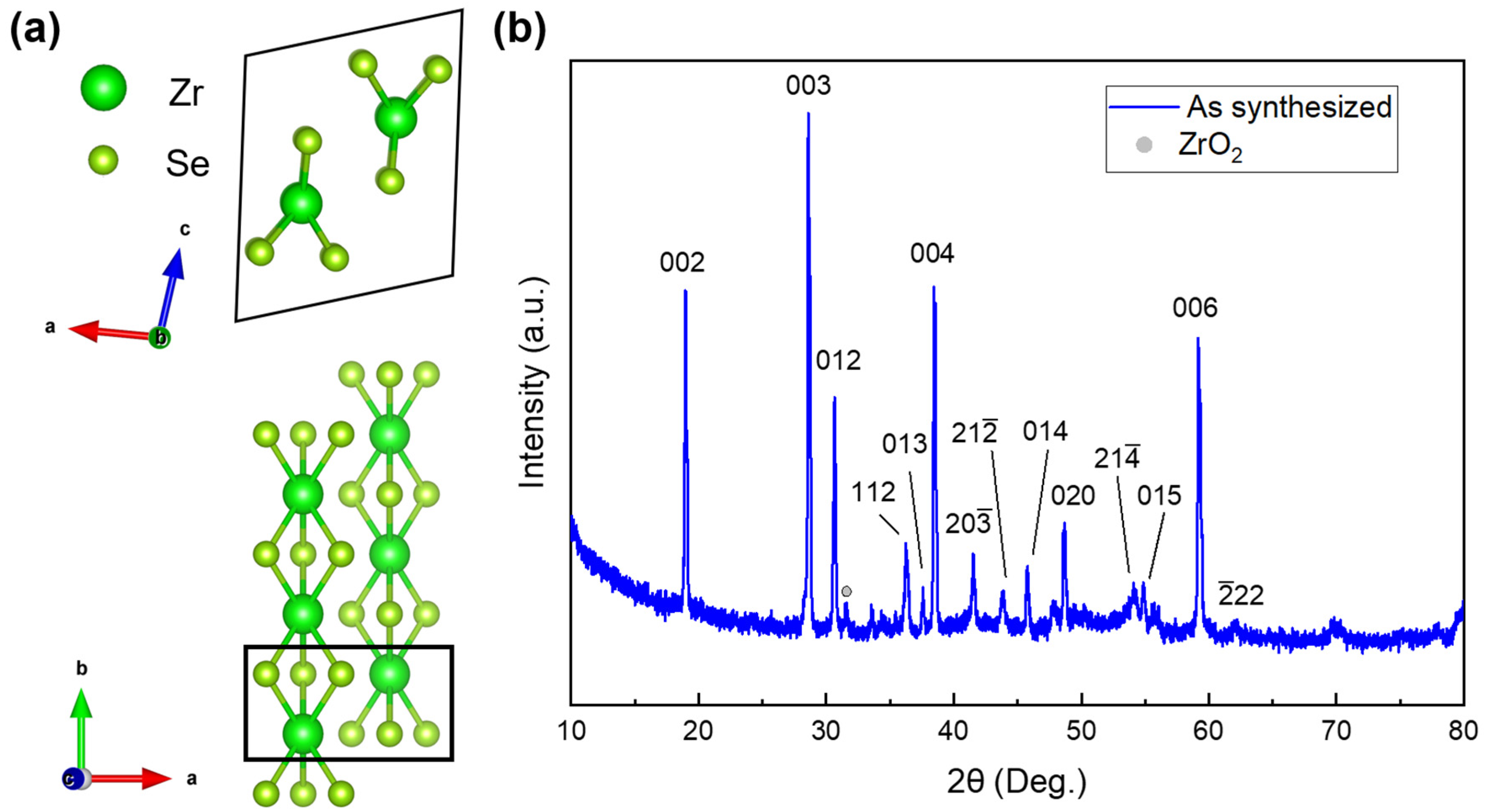
ZrSe3 exhibits a quasi-1D crystal structure with a monoclinic P21/m space group (No. 11), as shown in Figure 1a. Each Zr atom is bonded to six Se atoms, forming an edge-sharing triangle prism along the b-axis (1D chains). The chains are stacked along the a-axis via a weaker covalent bond and form a 2D layer in the ab plane. The layers are further stacked by weak vdW forces along the c-axis. The room-temperature powder XRD pattern of ZrSe3 (Figure 1b) is consistent with the previously reported results [33], indicating that the pure ZrSe3 phase was formed by CVT. The corresponding lattice parameters are a = 5.415(7) Å, b = 3.753(4) Å, and c = 9.473(8) Å, with α = γ = 90° and β = 97.72°. In addition, a small amount of ZrO2 phase was observed, which could be attributed to the residual oxygen gas during the crystal growth.
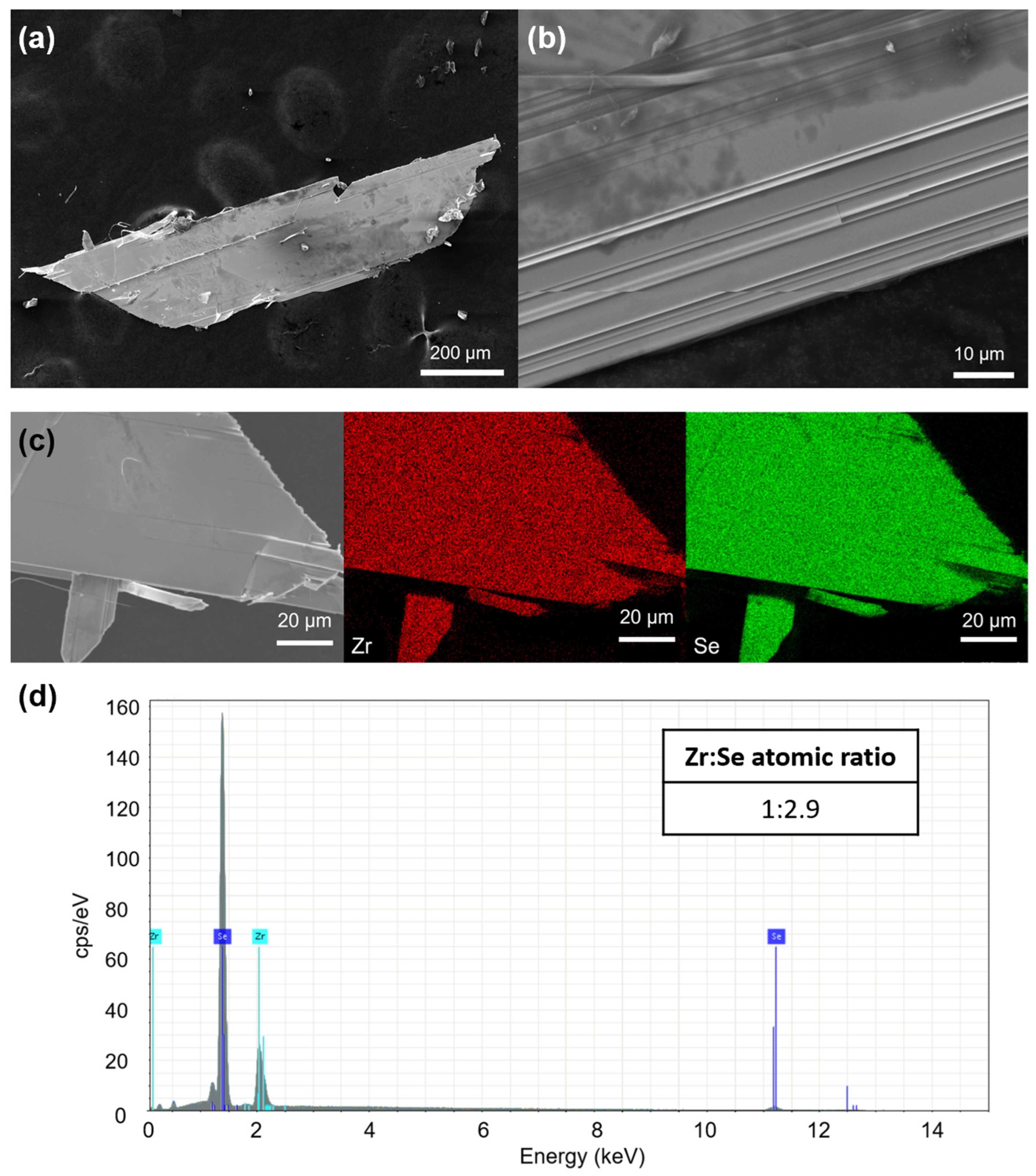
Figure 2a,b show the SEM images of the as-synthesized ZrSe3 flakes. The lateral dimension of the flakes is about 1 mm. Microribbons with a width of about 1 μm could be observed at the edge of large flakes, as shown in Figure 2b. The quasi-1D microribbons are stacked in parallel, forming flat 2D layers through additional covalent Zr-Se bonding. The energy-dispersive spectroscopy (EDS) elemental mapping of constituent elements (Zr and Se) confirmed the chemical homogeneity of the flake, as displayed in Figure 2c. The quantitative EDS analysis was performed based on Zr Lα and Se Lα lines, and the stoichiometric ratio of Zr:Se was found to be approximately 1:2.9, indicating that a slight Se deficiency may have existed in the sample. The chalcogen element deficiency has also been reported in other quasi-1D transitional metal chalcogenides grown using the CVT method [34,35]. Further study is needed to quantify the Se vacancies in ZrSe3.
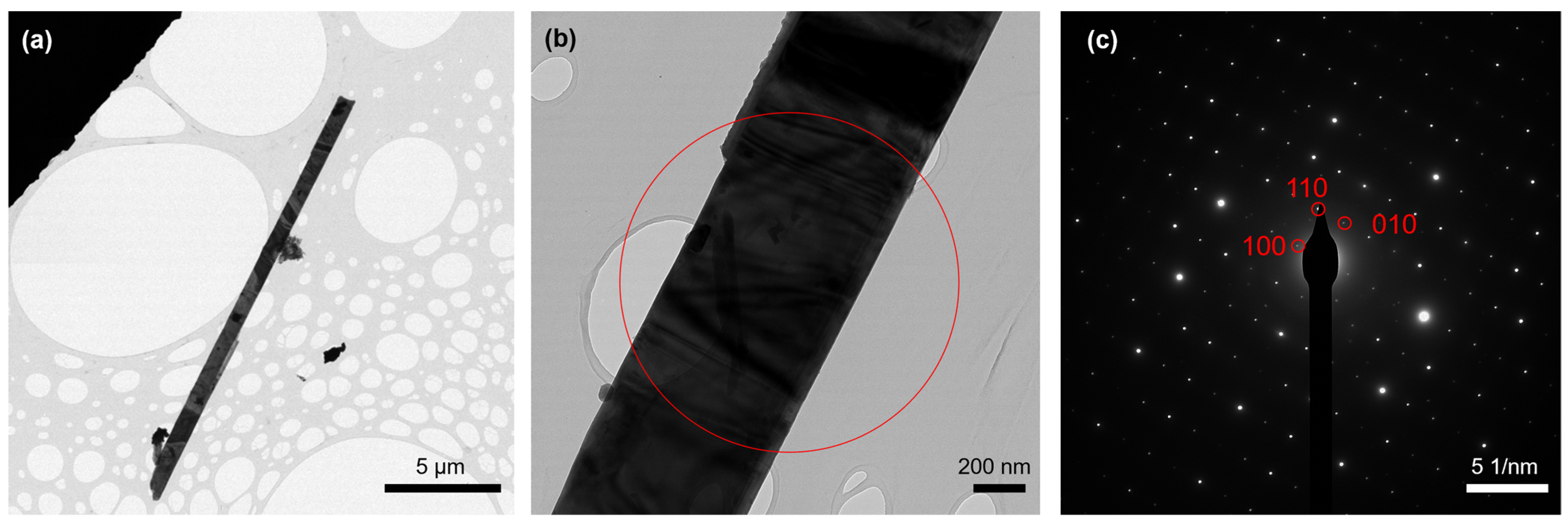
Due to the small exfoliation energy of ZrSe3 monolayers (0.37 J m−2) [36], ZrSe3 nanolayers were produced by mechanical exfoliation [30]. These findings motivated us to study the liquid-phase exfoliation of this compound. Figure 3a shows a typical microribbon of ZrSe3 with an in-plane dimension of 20 μm × 800 nm after liquid-phase exfoliation. The thickness of the microribbon was estimated to be less than 200 nm, verifying the effectiveness of liquid exfoliation to produce ZrSe3 nanolayers. The selected area electron diffraction (SAED) pattern (Figure 3c) could be indexed along the zone axis, confirming the microribbon was along the b-axis, which was the chain direction.
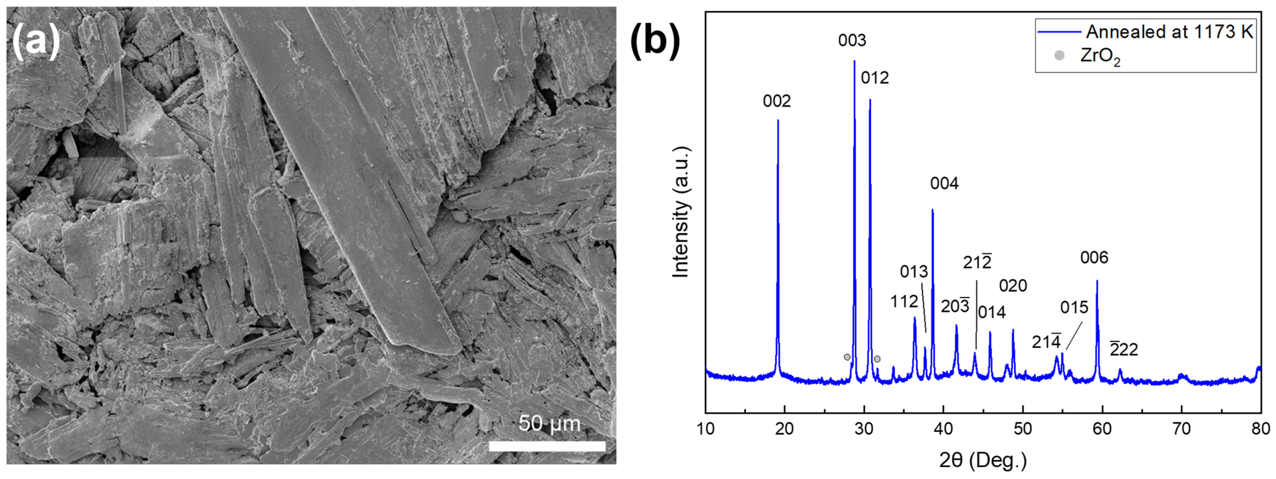
For the thermal property measurements, we prepared a polycrystalline ZrSe3 pellet by cold-pressing the CVT single crystals followed by annealing in a vacuum. Figure 4a shows the SEM image of the fracture surface of the pellet sample after cold-pressing. Microribbons were randomly distributed within the bulk sample. The average grain size was found to be about 4 μm. As shown in Figure 4b, no compositional change could be observed in the XRD pattern of the sample after annealing in a vacuum, indicating its chemical stability.
3.2. Optical and Thermal Properties
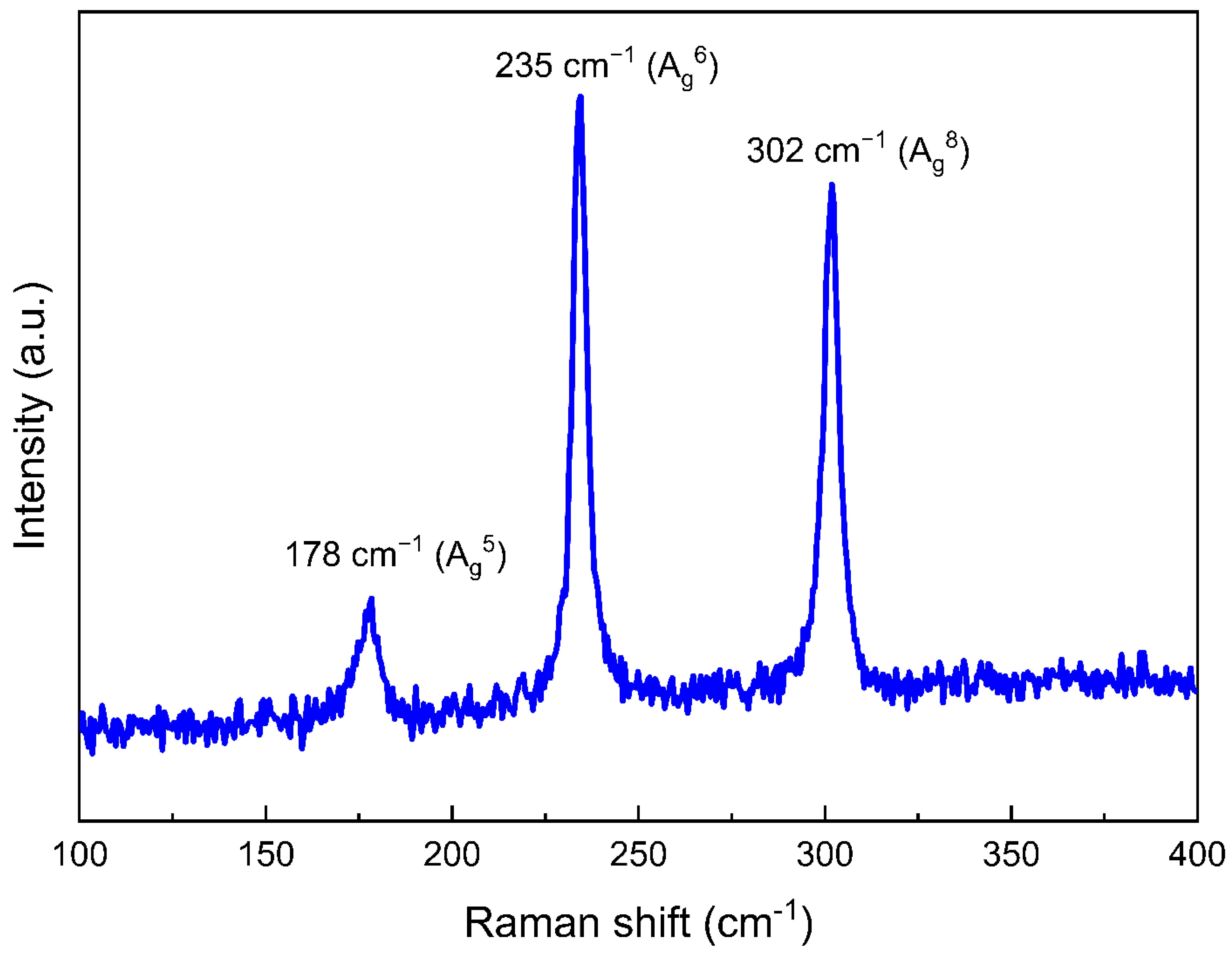
The Raman spectrum of ZrSe3 at 300 K shows three characteristic peaks at 178, 235, and 302 cm−1 in Figure 5. According to a previous Raman study on bulk ZrSe3, three similar peaks at 178, 230, and 300 cm−1 were also observed and were assigned to Ag5, Ag6, and Ag8 vibration modes, respectively [28]. Among them, Ag5 and Ag6 vibration modes correspond to the out-of-plane vibrations, and Ag8 is due to the in-plane vibration mode. The Ag5 mode consists of the movement of both Zr and Se atoms in the quasi-1D chains, while the Ag6 and Ag8 modes only consist of the movement of Se atoms.
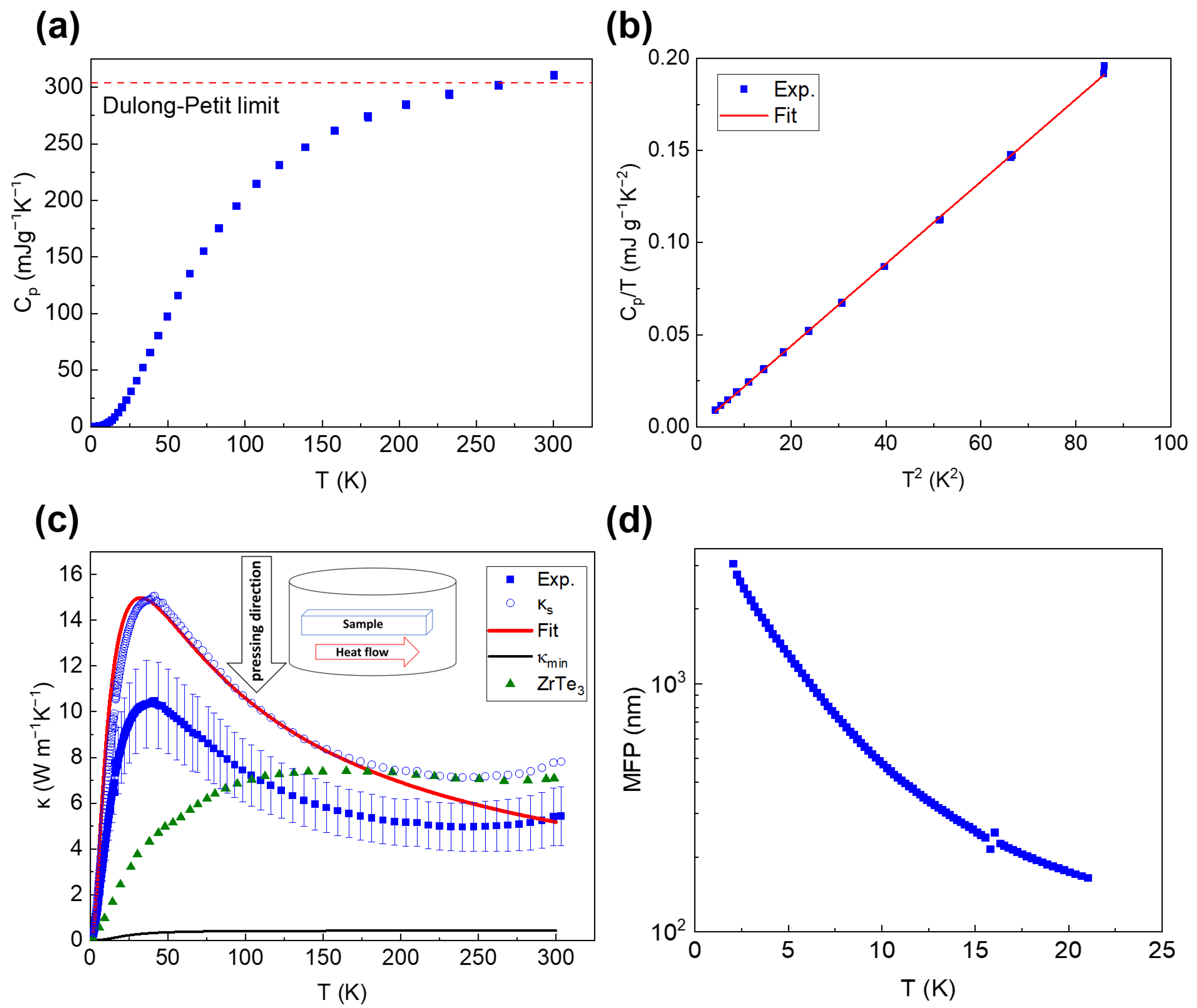
The specific heat of ZrSe3 from 2 to 300 K is shown in Figure 6a. The specific heat monotonically increased with temperature up to 300 K, and slightly exceeded the Dulong–Petit limit of 0.304 J g−1 K−1 above 280 K [37]. According to the Debye model [38], specific heat can be fitted via the following equation at low temperatures:
where γ is the electronic heat capacity coefficient, kB is the Boltzmann constant, N is the number of atoms per mole, T is the temperature, and θD is the Debye temperature. Cp/T versus T2 data below 9 K are shown in Figure 6b. The fitting led to a Debye temperature of 110 K with a sound velocity (vs) of 2122 m s−1, as listed in Table 1 together with other measured physical properties of ZrSe3. The obtained data are in good agreement with those from a previous study on ZrSe3 [39], where the reported Debye temperature and sound velocity were found to be 110 K and 2140 m s−1, respectively. The electronic heat capacity coefficient of ZrSe3 is negligible, in agreement with its semiconductor nature.
Figure 6c shows the measured thermal conductivity of the cold-pressed ZrSe3 sample in comparison with the data for a ZrTe3 polycrystal [40]. ZrTe3 has the same crystal structure as ZrSe3 but with larger lattice parameters. The thermal conductivity of ZrSe3 shows a clear peak at 40 K, while the thermal conductivity of ZrTe3 exhibits a broad plateau in the temperature range of 120−300 K. ZrSe3 shows a stronger temperature dependence of thermal conductivity at low temperatures compared with ZrTe3, indicating that the thermal conductivity of ZrSe3 is less affected by boundary scattering and defect scattering than ZrTe3. The resistivity of the ZrSe3 polycrystalline sample exceeds the measurement limit of the PPMS. From a previous study, the resistivity of ZrSe3 single crystal was reported to be 143.9 Ω cm at room temperature [27]. According to the Wiedemann–Franz law, with a Lorentz number of 2.44 × 10⁻⁸ V2 K−2, the calculated electronic thermal conductivity (κE) at 300 K is 5.1 × 10⁻⁶ W m−1 K−1, which is negligible compared with lattice thermal conductiity (κL).
At higher temperatures where phonon–phonon scattering dominates, the thermal conductivity of ZrSe3 is lower than that of ZrTe3, with values of 5.4 W m−1 K−1 and 7 W m−1 K−1 at 300 K, respectively. However, because the Te atom is heavier than the Se atom, the phonon spectrum of ZrTe3 should be narrower than that of ZrSe3, leading to smaller phonon velocities and stronger phonon–phonon scattering in ZrTe3. Thus, the thermal conductivity of ZrTe3 should be lower than that of ZrSe3, which seems to contradict our results. This discrepancy may have been caused by different synthesis parameters for the two samples, resulting in different porosities and texture effects. The calculated thermal conductivity of ZrTe3 along chain, cross-chain, and cross-plane directions are 9.6, 3.9, and 2.3 W m−1 K−1 at 300 K, respectively [24]. The polycrystalline ZrTe3 was reported to have texture effects with preferred orientation along the chain axis [40], showing an experimental thermal conductivity close to the calculated value along the chain direction. In addition, a small amount of ZrO2, observed by the XRD study, could enhance phonon scattering, and thus possibly decrease the thermal conductivity of ZrSe3.
3.3. Thermal Transport Analysis
The Debye model was used to analyze the thermal transport in ZrSe3. Before the Debye model fitting, the measured thermal conductivity needed to be corrected for porosity (f) because the cold-pressed sample was not dense enough and contained voids, as can be seen from Figure 4a. The porosity of the sample can be calculated from the following equation
where ρtheor is the theoretical density of ZrSe3. The porosity of ZrSe3 was calculated to be 18%.
According to the effective medium theory [42], the solid thermal conductivity () is related to the measured thermal conductivity as
The obtained of ZrSe3 is presented in Figure 6c. We fit the solid thermal conductivity of ZrSe3 from 2 to 200 K using the following Debye model [43],
where ℏ is the reduced Planck constant, x = ℏω/kBT, ω is phonon frequency, and τc is the lattice relaxation rate. The lattice relaxation rate consists of boundary scattering (τB), point defect scattering (τD) and Umklapp scattering (τU) contributions and can be expressed as
The relaxation rates for boundary scattering, point defect scattering, and Umklapp scattering, respectively, are given by
where L is the average grain size; and A and B are prefactors for point defect scattering and Umklapp scattering, respectively. Figure 6c shows the results of fitting the thermal conductivity to the Debye model. The obtained fitting parameters were L = 5.0 μm, A = 4.8 × 10−42 s3, and B = 2.1 × 10⁻¹⁸ s K−1. The obtained L value was consistent with the average grain size of about 4 μm from the SEM study (Figure 4a).
Extrapolating the fitting toward T > 200 K led to a deviation between the calculation and experimental data. Such a deviation could be attributed to the contribution of optical phonons to , which is not considered in the Debye model [44,45]. Debnath et al. calculated the phonon dispersion and thermal conductivity of ZrTe3 [24]. Several optical phonon modes were highly dispersive with large velocities. As a result, 33% of the lattice thermal conductivity was carried by optical phonons at room temperature. Similarly, Mortazavi et al. calculated the phonon dispersion of monolayer ZrSe3, and dispersive optical modes were also shown in the phonon dispersion [36]. These theoretical results are consistent with our findings, suggesting that the optical phonons in ZrSe3 can also contribute to thermal transport substantially.
In order to better understand the phonon transport in polycrystalline ZrSe3, acoustic phonon MFP can be calculated using the solid thermal conductivity as [46,47]
The calculated MFP of ZrSe3 up to 21 K is shown in Figure 6d. As temperature decreases, the calculated acoustic phonon MFP increases and reaches 3 μm at 2 K, consistent with the findings of the SEM study.
Furthermore, the minimum thermal conductivity (κmin) of ZrSe3 can be calculated according to the model developed by Cahill et al. [41] with the following equation:
where nA is the density of atoms. The κmin of ZrSe3 was found to be 0.43 W m−1 K−1 at 300 K, which is less than one-tenth of the measured value. As such, it is expected that the thermal conductivity of ZrSe3 can be further suppressed by nanostructuring [48] or defect engineering [49] for thermoelectric applications.
4. Conclusions
We report the crystal growth and thermal properties of quasi-1D vdW material ZrSe3. Millimeter-sized ZrSe3 flakes were grown by the CVT method. Due to the weak vdW bond along the c-axis and relative weak covalent bond along the a-axis, the flakes could be exfoliated into microribbons using the liquid-phase exfoliation method. The cold-pressed ZrSe3 sample exhibited a maximum thermal conductivity of 10.4 ± 1.9 W m−1 K−1 at 40 K and a room-temperature value of 5.4 ± 1.3 W m−1 K−1. The thermal transport analysis showed good agreement between the experimental data and Debye model fitting below 200 K, suggesting that the phonon transport in the polycrystalline sample was dominated by grain boundary, point defect, and Umklapp scattering. The high-temperature deviation between the fitting and experimental data could be attributed to the contribution of optical phonons. Combining the effective medium theory and Debye model, the acoustic phonon mean free path was calculated to be 3 μm at 2 K, consistent with the SEM observation. In addition, the analysis of low-temperature specific heat led to a Debye temperature of 110 K and an average sound velocity of 2122 m s−1. This study provides the first experimental investigation of thermal transport in ZrSe3 as well as preparation of ZrSe3 nanostructures using liquid-phase exfoliation, which can enable novel applications based on quasi-1D ZrSe3.
Author Contributions
Conceptualization, Y.X. and X.C.; methodology, Y.X. and S.G.; investigation, Y.X. and S.G.; writing—original draft preparation, Y.X.; writing—review and editing, Y.X., S.G. and X.C.; supervision, X.C.; project administration, X.C.; funding acquisition, X.C. All authors have read and agreed to the published version of the manuscript.
Funding
This work was supported by the National Science Foundation under Grant No. 2144328.
Data Availability Statement
The data presented in this study are available on request from the first author.
Conflicts of Interest
The authors declare no conflict of interest.
References
- Balandin, A.A.; Kargar, F.; Salguero, T.T.; Lake, R.K. One-dimensional van der Waals quantum materials. Mater. Today 2022, 55, 74–91. [Google Scholar] [CrossRef]
- Island, J.O.; Molina-Mendoza, A.J.; Barawi, M.; Biele, R.; Flores, E.; Clamagirand, J.M.; Ares, J.R.; Sanchez, C.; van der Zant, H.S.J.; D’Agosta, R.; et al. Electronics and optoelectronics of quasi-1D layered transition metal trichalcogenides. 2D Mater. 2017, 4, 022003. [Google Scholar] [CrossRef] [Green Version]
- Tsutsumi, K.; Takagaki, T.; Yamamoto, M.; Shiozaki, Y.; Ido, M.; Sambongi, T.; Yamaya, K.; Abe, Y. Direct Electron-Diffraction Evidence of Charge-Density-Wave Formation in NbSe3. Phys. Rev. Lett. 1977, 39, 1675. [Google Scholar] [CrossRef] [Green Version]
- Hodeau, J.L.; Marezio, M.; Roucau, C.; Ayroles, R.; Meerschaut, A.; Rouxel, J.; Monceau, P. Charge-density waves in NbSe3 at 145K: Crystal structures, X-ray and electron diffraction studies. J. Phys. C Solid State Phys. 1978, 11, 4117–4134. [Google Scholar] [CrossRef]
- Gorlova, I.G.; Pokrovskii, V.Y. Collective conduction mechanism in a quasi-one-dimensional TiS3 compound. Jetp. Lett. 2009, 90, 295–298. [Google Scholar] [CrossRef]
- Huang, C.; Zhang, E.Z.; Yuan, X.; Wang, W.Y.; Liu, Y.W.; Zhang, C.; Ling, J.W.; Liu, S.S.; Xiu, F.X. Tunable charge density wave in TiS3 nanoribbons. Chin. Phys. B 2017, 26, 10. [Google Scholar] [CrossRef]
- Denholme, S.J.; Yukawa, A.; Tsumura, K.; Nagao, M.; Tamura, R.; Watauchi, S.; Tanaka, I.; Takayanagi, H.; Miyakawa, N. Coexistence of superconductivity and charge-density wave in the quasi-one-dimensional material HfTe3. Sci. Rep. 2017, 7, 45217. [Google Scholar] [CrossRef] [PubMed] [Green Version]
- Hu, Y.W.; Zheng, F.P.; Ren, X.; Feng, J.; Li, Y. Charge density waves and phonon-electron coupling in ZrTe3. Phys. Rev. B 2015, 91, 10. [Google Scholar] [CrossRef] [Green Version]
- Felser, C.; Finckh, E.W.; Kleinke, H.; Rocker, F.; Tremel, W. Electronic properties of ZrTe3. J. Mater. Chem. 1998, 8, 1787–1798. [Google Scholar] [CrossRef]
- Hoesch, M.; Bosak, A.; Chernyshov, D.; Berger, H.; Krisch, M. Giant Kohn anomaly and the phase transition in charge density wave ZrTe3. Phys. Rev. Lett. 2009, 102, 086402. [Google Scholar] [CrossRef]
- Liu, L.; Zhu, C.; Liu, Z.Y.; Deng, H.; Zhou, X.B.; Li, Y.; Sun, Y.; Huang, X.; Li, S.; Du, X.; et al. Thermal Dynamics of Charge Density Wave Pinning in ZrTe3. Phys. Rev. Lett. 2021, 126, 256401. [Google Scholar] [CrossRef] [PubMed]
- Monceau, P.; Peyrard, J.; Richard, J.; Molinie, P. Superconductivity of Linear Trichalcogenide NbSe3 under Pressure. Phys. Rev. Lett. 1977, 39, 161–164. [Google Scholar] [CrossRef]
- Yue, B.; Zhong, W.; Deng, W.; Wen, T.; Wang, Y.; Yin, Y.; Shan, P.; Yu, X.; Hong, F. Insulator-to-superconductor transition in quasi-one-dimensional HfS3 under pressure. arXiv 2021, arXiv:2111.02060. [Google Scholar]
- Mayorga-Martinez, C.C.; Sofer, Z.; Luxa, J.; Huber, S.; Sedmidubsky, D.; Brazda, P.; Palatinus, L.; Mikulics, M.; Lazar, P.; Medlin, R.; et al. TaS3 Nanofibers: Layered Trichalcogenide for High-Performance Electronic and Sensing Devices. ACS Nano 2018, 12, 464–473. [Google Scholar] [CrossRef]
- Xiong, W.W.; Chen, J.Q.; Wu, X.C.; Zhu, J.J. Individual HfS3 nanobelt for field-effect transistor and high performance visible-light detector. J. Mater. Chem. C 2014, 2, 7392–7395. [Google Scholar] [CrossRef]
- Dai, J.; Li, M.; Zeng, X.C. Group IVB transition metal trichalcogenides: A new class of 2D layered materials beyond graphene. Wiley Interdiscip. Rev.-Comput. Mol. Sci. 2016, 6, 211–222. [Google Scholar] [CrossRef]
- Dowben, P.A.; Binek, C.; Zhang, K.; Wang, L.; Mei, W.-N.; Bird, J.P.; Singisetti, U.; Hong, X.; Wang, K.L.; Nikonov, D. Towards a strong spin–orbit coupling magnetoelectric transistor. IEEE J. Explor. Solid-State Comput. Devices Circuits 2018, 4, 1–9. [Google Scholar] [CrossRef]
- Island, J.O.; Biele, R.; Barawi, M.; Clamagirand, J.M.; Ares, J.R.; Sanchez, C.; van der Zant, H.S.; Ferrer, I.J.; D’Agosta, R.; Castellanos-Gomez, A. Titanium trisulfide (TiS3): A 2D semiconductor with quasi-1D optical and electronic properties. Sci. Rep. 2016, 6, 22214. [Google Scholar] [CrossRef] [PubMed] [Green Version]
- Wang, J.; Jiang, C.Z.; Li, W.Q.; Xiao, X.H. Anisotropic Low-Dimensional Materials for Polarization-Sensitive Photodetectors: From Materials to Devices. Adv. Opt. Mater. 2022, 10, 2102436. [Google Scholar] [CrossRef]
- Biele, R.; D’Agosta, R. Transport coefficients of layered TiS3. Phys. Rev. Mater. 2022, 6, 8. [Google Scholar] [CrossRef]
- Sakuma, T.; Nishino, S.; Miyata, M.; Koyano, M. Thermoelectric Properties for a Suspended Microribbon of Quasi-One-Dimensional TiS3. J. Electron. Mater. 2018, 47, 3177–3183. [Google Scholar] [CrossRef]
- Zhang, J.; Liu, X.; Wen, Y.; Shi, L.; Chen, R.; Liu, H.; Shan, B. Titanium Trisulfide Monolayer as a Potential Thermoelectric Material: A First-Principles-Based Boltzmann Transport Study. ACS Appl. Mater. Interfaces 2017, 9, 2509–2515. [Google Scholar] [CrossRef] [PubMed]
- Liu, H.; Yu, X.; Wu, K.; Gao, Y.; Tongay, S.; Javey, A.; Chen, L.; Hong, J.; Wu, J. Extreme In-Plane Thermal Conductivity Anisotropy in Titanium Trisulfide Caused by Heat-Carrying Optical Phonons. Nano Lett. 2020, 20, 5221–5227. [Google Scholar] [CrossRef] [PubMed]
- Debnath, T.; Debnath, B.; Lake, R.K. Thermal conductivity of the quasi-one-dimensional materials TaSe3 and ZrTe3. Phys. Rev. Mater. 2021, 5, 034010. [Google Scholar] [CrossRef]
- Yang, L.; Tao, Y.; Zhu, Y.; Akter, M.; Wang, K.; Pan, Z.; Zhao, Y.; Zhang, Q.; Xu, Y.Q.; Chen, R.; et al. Observation of superdiffusive phonon transport in aligned atomic chains. Nat. Nanotechnol. 2021, 16, 764–768. [Google Scholar] [CrossRef]
- Kurita, S.; Tanaka, M.; Lévy, F. Optical spectra near the band edge of ZrS3 and ZrSe3. Phys. Rev. B 1993, 48, 1356. [Google Scholar] [CrossRef]
- Patel, K.; Prajapati, J.; Vaidya, R.; Patel, S.G. Optical and electrical properties of ZrSe3 single crystals grown by chemical vapour transport technique. Bull. Mater. Sci. 2005, 28, 405–410. [Google Scholar] [CrossRef] [Green Version]
- Osada, K.; Bae, S.; Tanaka, M.; Raebiger, H.; Shudo, K.; Suzuki, T. Phonon Properties of Few-Layer Crystals of Quasi-One-Dimensional ZrS3 and ZrSe3. J. Phys. Chem. C 2016, 120, 4653–4659. [Google Scholar] [CrossRef]
- Wang, X.; Xiong, T.; Xin, K.; Yang, J.; Liu, Y.; Zhao, Z.; Liu, J.; Wei, Z. Polarization sensitive photodetector based on quasi-1D ZrSe3. J. Semicond. 2022, 43, 102001. [Google Scholar] [CrossRef]
- Li, H.; Sanchez-Santolino, G.; Puebla, S.; Frisenda, R.; Al-Enizi, A.M.; Nafady, A.; D’Agosta, R.; Castellanos-Gomez, A. Strongly Anisotropic Strain-Tunability of Excitons in Exfoliated ZrSe3. Adv. Mater. 2022, 34, 2103571. [Google Scholar] [CrossRef]
- Zhu, Y.H.; Chen, Q.; Wu, H.J.; Liang, J.; Tian, M.M.; Jiang, W.; Wang, J.C.; Li, R.X.; Li, S.K.; Huang, Z.C.; et al. Large spin hall conductivity in low-symmetry semiconductor ZrSe3. J. Alloys Compd. 2022, 918, 165579. [Google Scholar] [CrossRef]
- Zhou, Z.; Liu, H.; Fan, D.; Cao, G.; Sheng, C. High Thermoelectric Performance Originating from the Grooved Bands in the ZrSe3 Monolayer. ACS Appl. Mater. Interfaces 2018, 10, 37031–37037. [Google Scholar] [CrossRef] [Green Version]
- Furuseth, S.; Brattås, L.; Kjekshus, A.; Andresen, A.F.; Fischer, P. On the Crystal Structures of TiS3, ZrS3, ZrSe3, ZrTe3, HfS3, and HfSe3. Acta Chem. Scand. 1975, 29a, 623–631. [Google Scholar] [CrossRef] [Green Version]
- Barani, Z.; Kargar, F.; Ghafouri, Y.; Ghosh, S.; Godziszewski, K.; Baraghani, S.; Yashchyshyn, Y.; Cywiński, G.; Rumyantsev, S.; Salguero, T.T. Electrically Insulating Flexible Films with Quasi-1D Van Der Waals Fillers as Efficient Electromagnetic Shields in the GHz and Sub-THz Frequency Bands. Adv. Mater. 2021, 33, 2007286. [Google Scholar] [CrossRef] [PubMed]
- Shahi, P.; Singh, D.J.; Sun, J.P.; Zhao, L.X.; Chen, G.F.; Lv, Y.Y.; Li, J.; Yan, J.Q.; Mandrus, D.G.; Cheng, J.G. Bipolar Conduction as the Possible Origin of the Electronic Transition in Pentatellurides: Metallic vs Semiconducting Behavior. Phys. Rev. X 2018, 8, 021055. [Google Scholar] [CrossRef] [Green Version]
- Mortazavi, B.; Shojaei, F.; Yagmurcukardes, M.; Makaremi, M.; Zhuang, X.Y. A Theoretical Investigation on the Physical Properties of Zirconium Trichalcogenides, ZrS3, ZrSe3 and ZrTe3 Monolayers. Energies 2022, 15, 5479. [Google Scholar] [CrossRef]
- Petit, A.; Dulong, P. Study on the measurement of specific heat of solids. Ann. Chim. Phys. 1819, 10, 395. [Google Scholar]
- Debye, P. Zur Theorie der spezifischen Wärmen. Ann. Der. Phys. 1912, 344, 789–839. [Google Scholar] [CrossRef] [Green Version]
- Provencher, R.; Ayache, C.; Jandl, S.; Jaygerin, J.P. Low-Temperature Specific-Heats of ZrSe3 and ZrS3. Solid State Commun. 1986, 59, 553–556. [Google Scholar] [CrossRef]
- Hooda, M.K.; Tripathi, T.S.; Yadav, C.S. Semiconducting nature and thermal transport studies of ZrTe3. J. Alloys Compd. 2019, 785, 603–609. [Google Scholar] [CrossRef] [Green Version]
- Cahill, D.G.; Watson, S.K.; Pohl, R.O. Lower limit to the thermal conductivity of disordered crystals. Phys. Rev. B Condens. Matter. 1992, 46, 6131–6140. [Google Scholar] [CrossRef] [PubMed]
- Nan, C.-W.; Birringer, R.; Clarke, D.R.; Gleiter, H. Effective thermal conductivity of particulate composites with interfacial thermal resistance. J. Appl. Phys. 1997, 81, 6692–6699. [Google Scholar] [CrossRef]
- Callaway, J. Model for Lattice Thermal Conductivity at Low Temperatures. Phys. Rev. 1959, 113, 1046–1051. [Google Scholar] [CrossRef]
- Che, H.L.; Shi, J.; Wu, J.C.; Rao, X.; Liu, X.G.; Zhao, X.; Sun, X.F. Thermal conductivity of Ca3Co2O6 single crystals. AIP Adv. 2018, 8, 055811. [Google Scholar] [CrossRef]
- Cheng, J.G.; Zhou, J.S.; Goodenough, J.B. Thermal conductivity, electron transport, and magnetic properties of single-crystal Ca3Co2O6. Phys. Rev. B 2009, 79, 184414. [Google Scholar] [CrossRef]
- Chen, X.; Weathers, A.; Moore, A.; Zhou, J.S.; Shi, L. Thermoelectric Properties of Cold-Pressed Higher Manganese Silicides for Waste Heat Recovery. J. Electron. Mater. 2012, 41, 1564–1572. [Google Scholar] [CrossRef]
- Li, S.C.; Guo, S.C.; Xu, Y.M.; Zhou, J.S.; Chen, X. Role of Grain Size on Magnon and Phonon Thermal Transport in the Spin Ladder Compound Ca9La5Cu24O41. Acs Appl. Electron. Mater. 2022, 4, 787–794. [Google Scholar] [CrossRef]
- Chen, X.; Shi, L.; Zhou, J.; Goodenough, J.B. Effects of ball milling on microstructures and thermoelectric properties of higher manganese silicides. J. Alloys Compd. 2015, 641, 30–36. [Google Scholar] [CrossRef] [Green Version]
- Chen, X.; Girard, S.N.; Meng, F.; Lara-Curzio, E.; Jin, S.; Goodenough, J.B.; Zhou, J.; Shi, L. Approaching the Minimum Thermal Conductivity in Rhenium-Substituted Higher Manganese Silicides. Adv. Energy Mater. 2014, 4, 1400452. [Google Scholar] [CrossRef]
Figure 1.
(a) Crystal structure of ZrSe3. Each Zr atom bonds to six neighbor Se atoms, forming a triagonal prism. (b) Indexed powder XRD pattern of the ZrSe3 sample.
Figure 1.
(a) Crystal structure of ZrSe3. Each Zr atom bonds to six neighbor Se atoms, forming a triagonal prism. (b) Indexed powder XRD pattern of the ZrSe3 sample.

Figure 2.
(a,b) SEM images of ZrSe3 after CVT. (c) EDS elemental mapping of Zr and Se in a ZrSe3 flake. (d) EDS spectrum of ZrSe3.
Figure 2.
(a,b) SEM images of ZrSe3 after CVT. (c) EDS elemental mapping of Zr and Se in a ZrSe3 flake. (d) EDS spectrum of ZrSe3.

Figure 3.
(a,b) TEM images of the ZrSe3 sample after liquid-phase exfoliation. The circle in (b) indicates the region for electron diffraction. (c) The corresponding SAED pattern obtained along zone axis.
Figure 3.
(a,b) TEM images of the ZrSe3 sample after liquid-phase exfoliation. The circle in (b) indicates the region for electron diffraction. (c) The corresponding SAED pattern obtained along zone axis.

Figure 4.
(a) SEM image of the ZrSe3 sample after cold-pressing showing the fracture surface perpendicular to the press direction. (b) Powder XRD pattern of ZrSe3 after annealing at 1173 K in vacuum.
Figure 4.
(a) SEM image of the ZrSe3 sample after cold-pressing showing the fracture surface perpendicular to the press direction. (b) Powder XRD pattern of ZrSe3 after annealing at 1173 K in vacuum.

Figure 5.
Raman spectrum of ZrSe3 at 300 K.

Figure 6.
(a) Specific heat as a function of temperature for ZrSe3. The high-temperature limit was calculated using the Dulong–Petit law. (b) Cp/T versus T2 at low temperatures. (c) Thermal conductivity of ZrSe3 as a function of temperature. The solid thermal conductivity was calculated by correcting the porosity effect. The experimental data for ZrTe3 are included for comparison [40]. The solid thermal conductivity was fitted using the Debye model. The minimum thermal conductivity was calculated via the Cahill model [41]. The inset of (c) is a schematic illustration of the thermal conductivity measurement direction. Reprinted/adapted with permission from Ref. [40]. Copyright 2019, Elsevier. (d) Phonon MFP of the cold-pressed sample as a function of temperature below 21 K.


Table 1.
Experimentally measured physical properties of ZrSe3.
| Sample | ρ (g cm−3) | Cp (J g−1 K−1) | θD (K) | vs (m s−1) | κ (W m−1 K−1) | κmax (W m−1 K−1) |
|---|---|---|---|---|---|---|
| ZrSe3 | 4.27 | 0.311 (300 K) | 110 | 2122 | 5.4 ± 1.3 (300 K) | 10.4 ± 1.9 (40 K) |
Publisher’s Note: MDPI stays neutral with regard to jurisdictional claims in published maps and institutional affiliations. |
© 2022 by the authors. Licensee MDPI, Basel, Switzerland. This article is an open access article distributed under the terms and conditions of the Creative Commons Attribution (CC BY) license (https://creativecommons.org/licenses/by/4.0/).
Share and Cite
MDPI and ACS Style
Xu, Y.; Guo, S.; Chen, X. Crystal Growth and Thermal Properties of Quasi-One-Dimensional van der Waals Material ZrSe3. Micromachines 2022, 13, 1994. https://doi.org/10.3390/mi13111994
AMA Style
Xu Y, Guo S, Chen X. Crystal Growth and Thermal Properties of Quasi-One-Dimensional van der Waals Material ZrSe3. Micromachines. 2022; 13(11):1994. https://doi.org/10.3390/mi13111994
Chicago/Turabian StyleXu, Youming, Shucheng Guo, and Xi Chen. 2022. "Crystal Growth and Thermal Properties of Quasi-One-Dimensional van der Waals Material ZrSe3" Micromachines 13, no. 11: 1994. https://doi.org/10.3390/mi13111994
Note that from the first issue of 2016, this journal uses article numbers instead of page numbers. See further details here.