
Heterogeneous Wafer Bonding Technology and Thin-Film Transfer Technology-Enabling Platform for the Next Generation Applications beyond 5G


Abstract
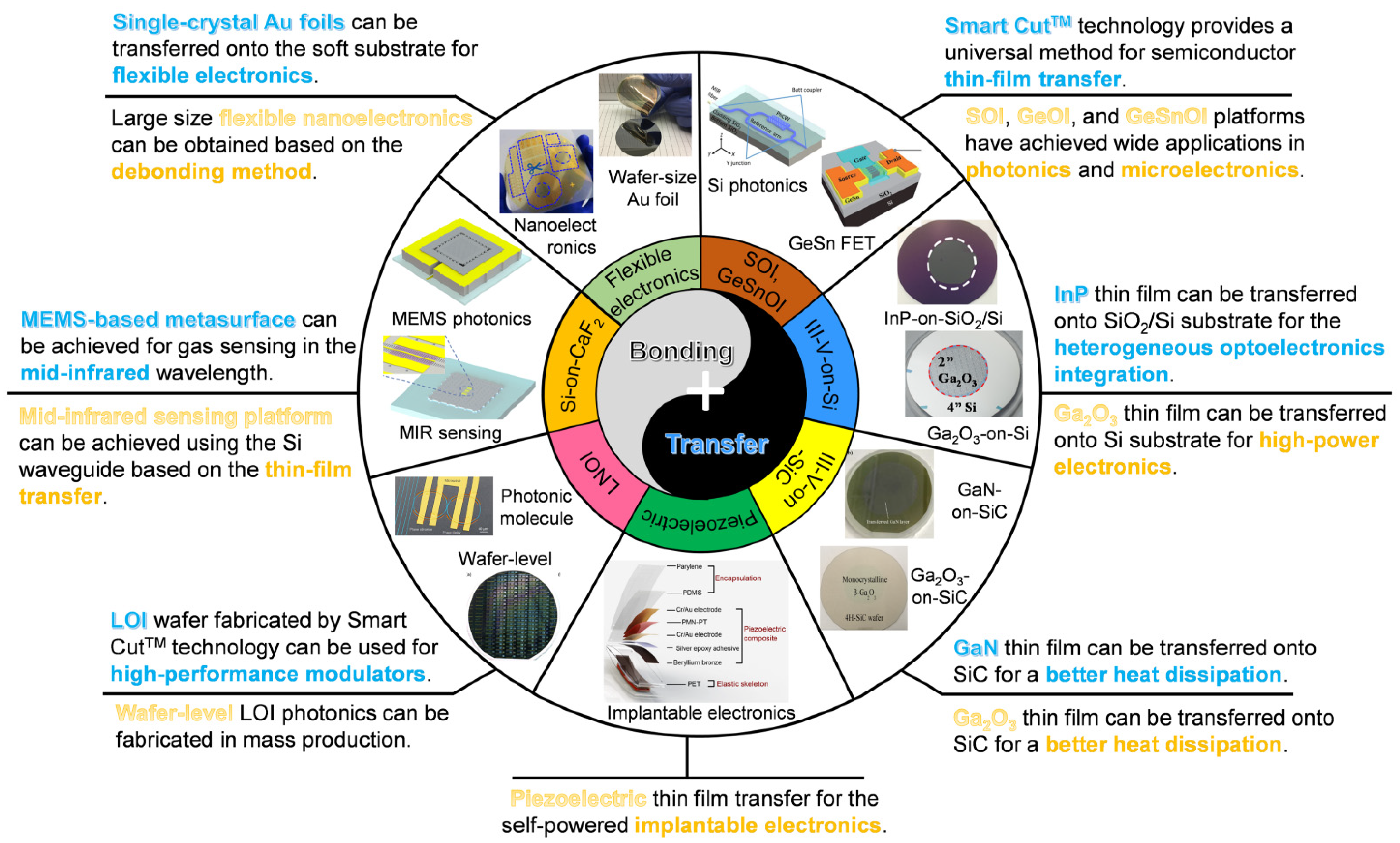
:1. Introduction
2. Fabrication of Si- and Ge-Based Thin Film-on-Insulators via Wafer Bonding Method
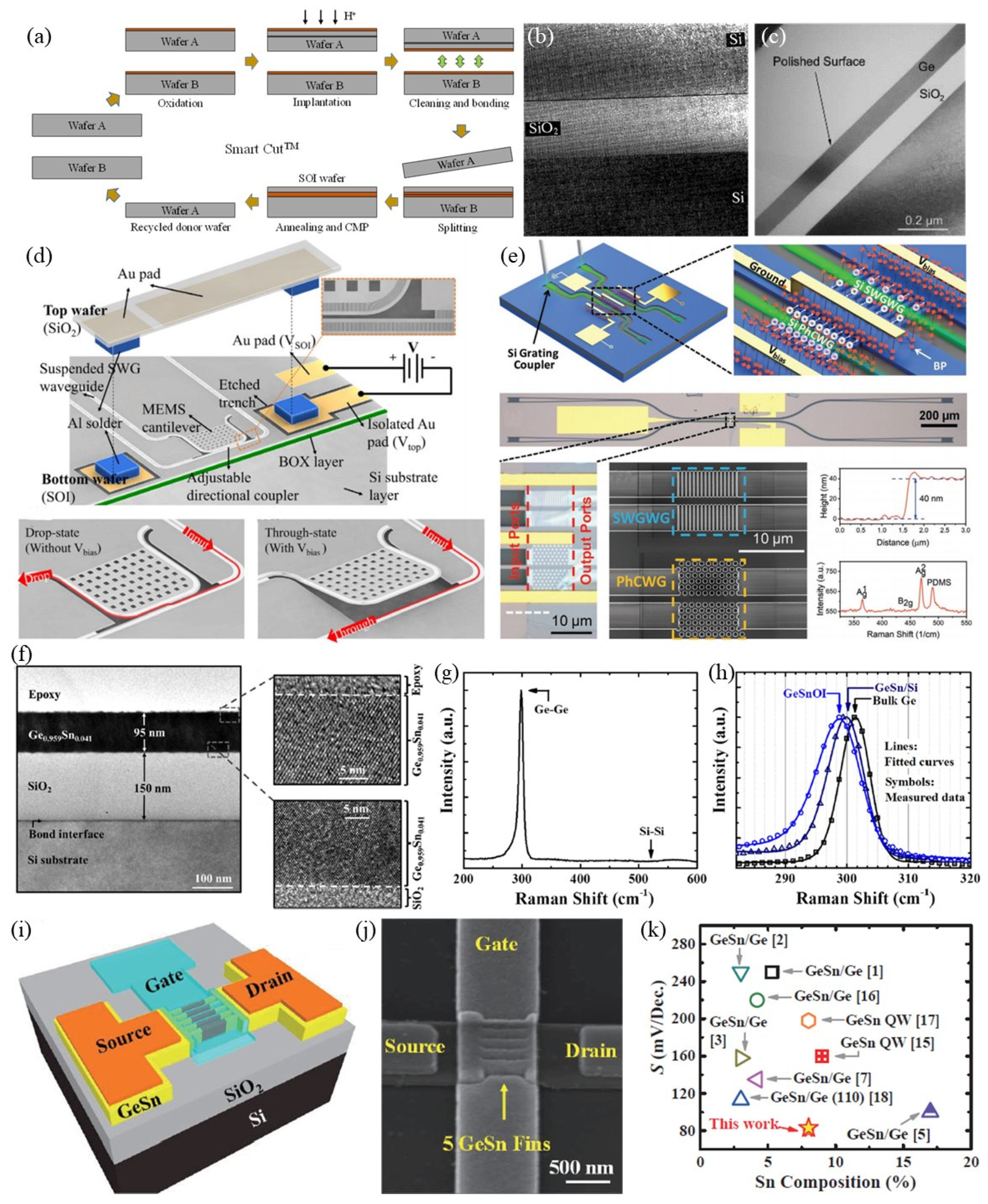
2.1. Smart CutTM Technology for the Fabrication of Si-on-Insulator and Its Applications
2.2. GeSn-on-Insulator Platform Fabrication and Its Applications in FETs
3. Heterogeneous Bonding for III-V and Wide Bandgap Semiconductor Thin-Film Transfer onto Si Substrate
3.1. InP Thin-Film Transfer Based on the Modified Smart CutTM Technology
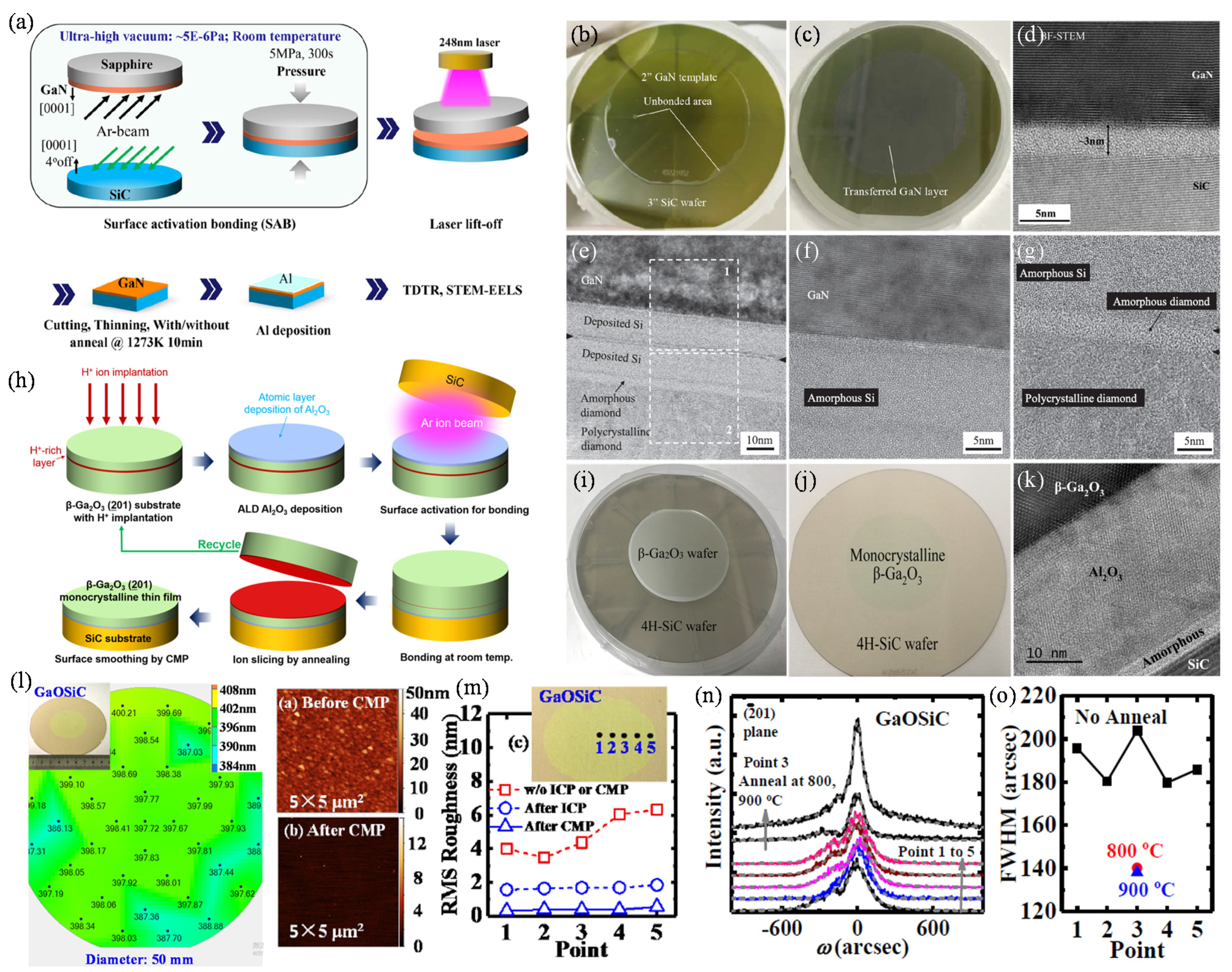
3.2. Wide Bandgap Semiconductor Thin-Film Transfer and Its Applications in MOSFETs
4. Heterogeneous Bonding for Wide-Bandgap Semiconductors Thin-Film Transfer onto SiC or Diamond Substrates for High Heat Dissipation
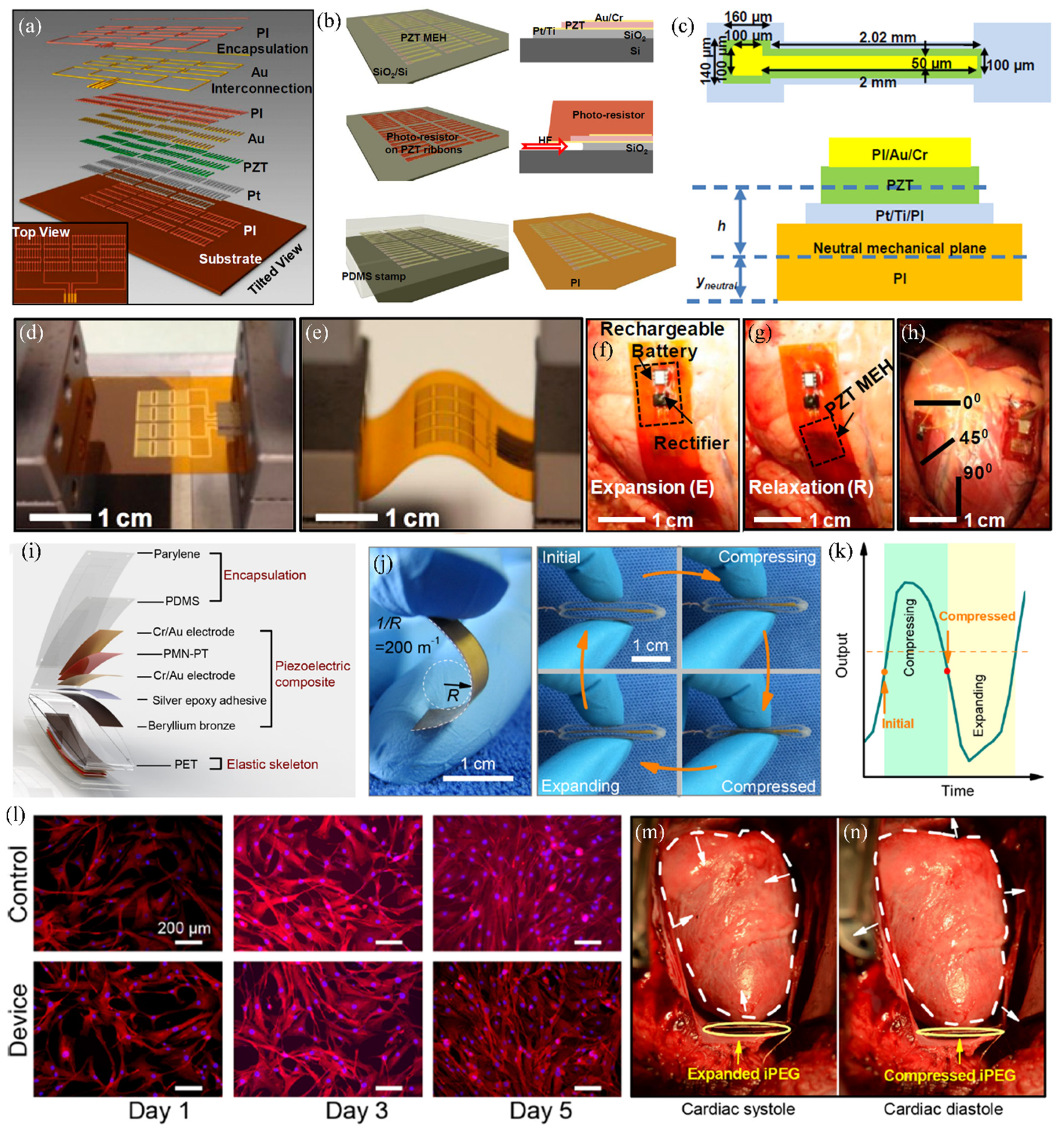
5. Piezoelectric Thin Transfer for the Self-Powered Implantable Electronics
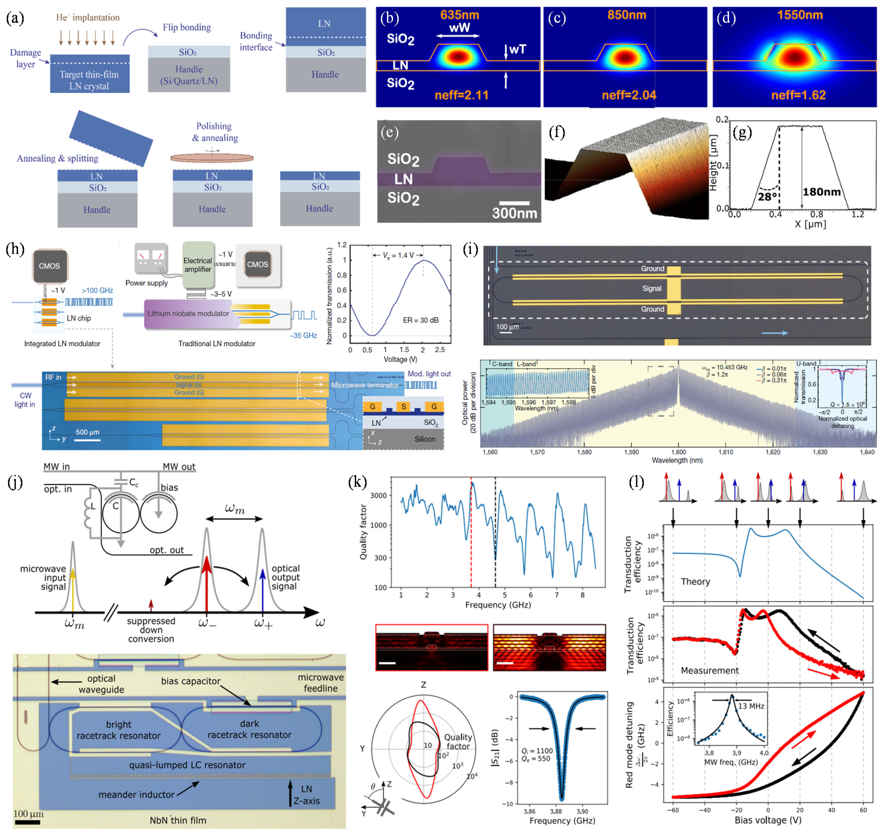
6. LiNbO3 Thin-Film Transfer for High-Performance Electro-Optical Modulators
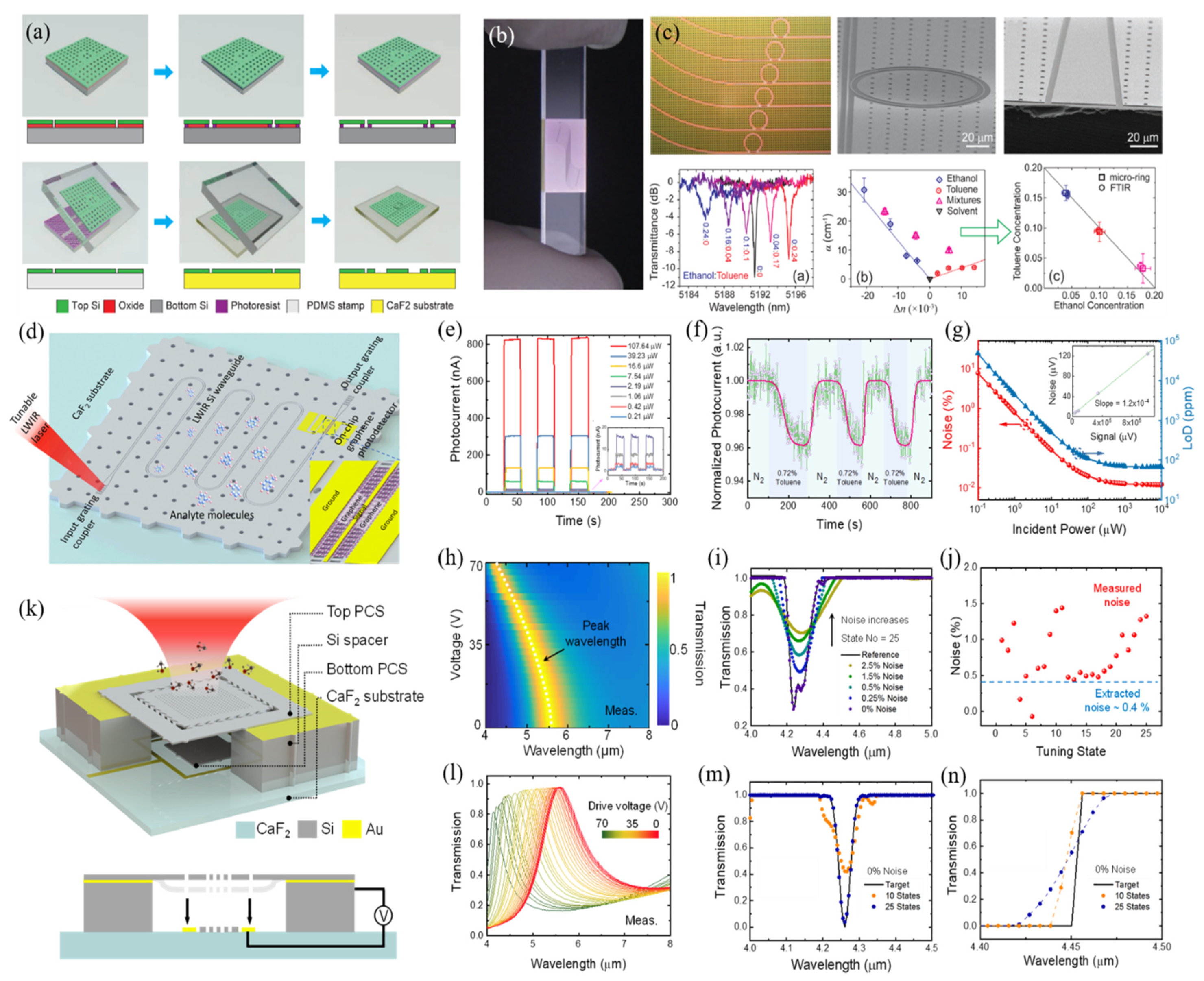
7. Si-on-CaF2 Platform Fabrication for MIR Sensors
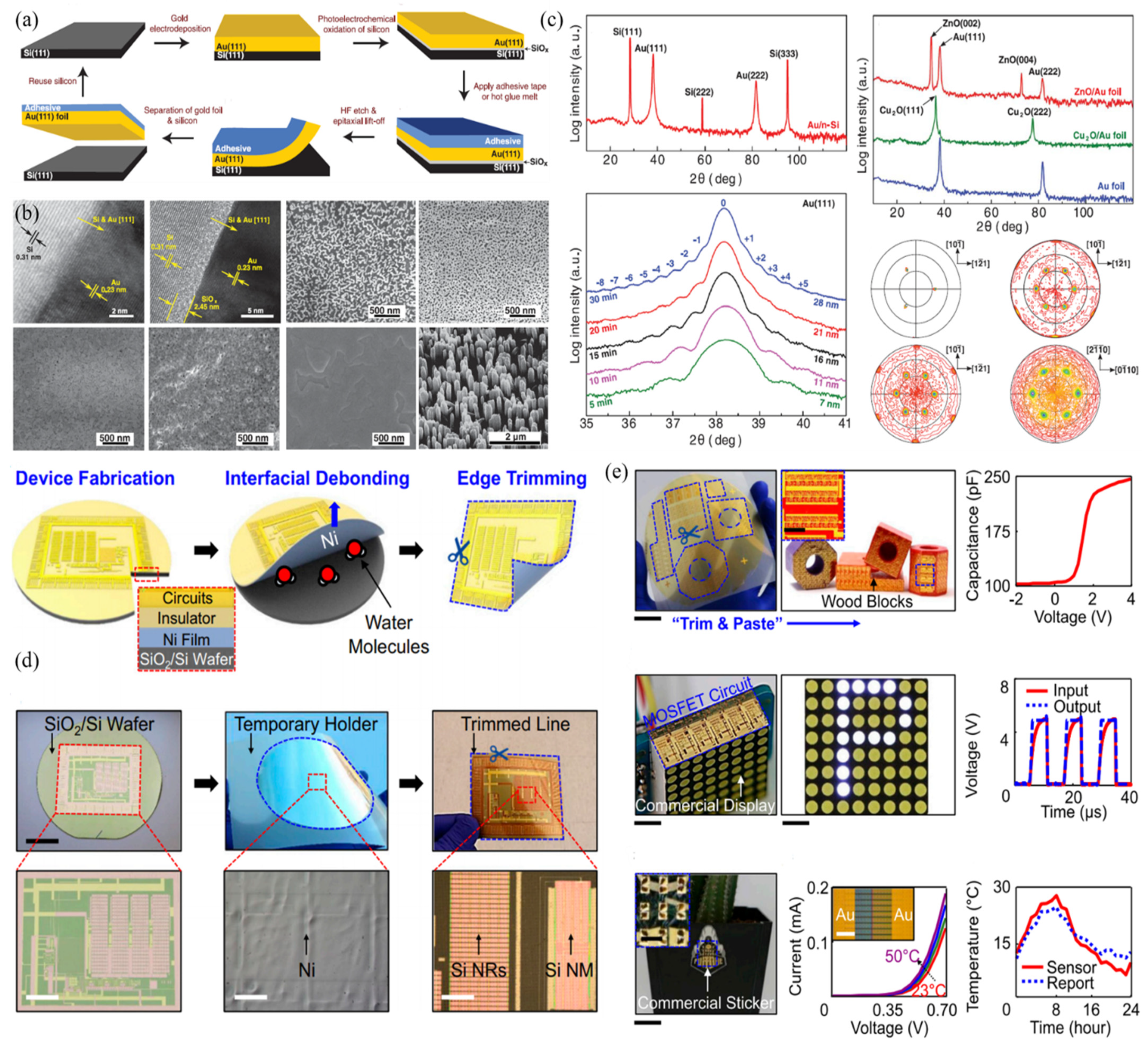
8. High-Quality Thin Film Obtained via the Debonding Method for Flexible Electronics
9. Concluding Remarks and Perspectives
Author Contributions
Funding
Conflicts of Interest
References
- Lee, C.; Xie, J. Design and Optimization of Wafer Bonding Packaged Microelectromechanical Systems Thermoelectric Power Generators with Heat Dissipation Path. J. Vac. Sci. Technol. B Microelectron. Nanom. Struct. 2009, 27, 1267. [Google Scholar] [CrossRef]
- Lee, C.; Huang, W.-F.; Shie, J.-S. Wafer Bonding by Low-Temperature Soldering. Sens. Actuators A Phys. 2000, 85, 330–334. [Google Scholar] [CrossRef]
- Lee, C.; Yu, A.; Yan, L.; Wang, H.; He, J.H.; Zhang, Q.X.; Lau, J.H. Characterization of Intermediate In/Ag Layers of Low Temperature Fluxless Solder Based Wafer Bonding for MEMS Packaging. Sens. Actuators A Phys. 2009, 154, 85–91. [Google Scholar] [CrossRef]
- Niklaus, F.; Stemme, G.; Lu, J.Q.; Gutmann, R.J. Adhesive Wafer Bonding. J. Appl. Phys. 2006, 99, 031101. [Google Scholar] [CrossRef]
- Lin, Y.-S.; Xu, Z. Reconfigurable Metamaterials for Optoelectronic Applications. Int. J. Optomechatronics 2020, 14, 78–93. [Google Scholar] [CrossRef]
- Yu, D.Q.; Lee, C.; Yan, L.L.; Thew, M.L.; Lau, J.H. Characterization and Reliability Study of Low Temperature Hermetic Wafer Level Bonding Using In/Sn Interlayer and Cu/Ni/Au Metallization. J. Alloy. Compd. 2009, 485, 444–450. [Google Scholar] [CrossRef]
- Da-Quan, Y.; Li, L.Y.; Chengkuo, L.; Won, K.C.; Thew, S.; Chin, K.F.; Lau, J.H. Wafer-Level Hermetic Bonding Using Sn/In and Cu/Ti/Au Metallization. IEEE Trans. Compon. Packag. Technol. 2009, 32, 926–934. [Google Scholar] [CrossRef] [Green Version]
- Tian, R.; Hang, C.; Tian, Y.; Wu, B.; Liu, Y.; Zhao, J. Interfacial Intermetallic Compound Growth in Sn-3Ag-0.5Cu/Cu Solder Joints Induced by Stress Gradient at Cryogenic Temperatures. J. Alloy. Compd. 2019, 800, 180–190. [Google Scholar]
- Made, R.I.; Gan, C.L.; Yan, L.L.; Yu, A.; Yoon, S.W.; Lau, J.H.; Lee, C. Study of Low-Temperature Thermocompression Bonding in Ag-In Solder for Packaging Applications. J. Electron. Mater. 2009, 38, 365–371. [Google Scholar] [CrossRef]
- Tian, R.; Hang, C.; Tian, Y.; Feng, J. Brittle Fracture Induced by Phase Transformation of Ni-Cu-Sn Intermetallic Compounds in Sn-3Ag-0.5Cu/Ni Solder Joints under Extreme Temperature Environment. J. Alloy. Compd. 2019, 777, 463–471. [Google Scholar] [CrossRef]
- Cheng, Z.; Mu, F.; Yates, L.; Suga, T.; Graham, S. Interfacial Thermal Conductance across Room-Temperature-Bonded GaN/Diamond Interfaces for GaN-on-Diamond Devices. ACS Appl. Mater. Interfaces 2020, 12, 8376–8384. [Google Scholar] [CrossRef]
- Mu, F.; Cheng, Z.; Shi, J.; Shin, S.; Xu, B.; Shiomi, J.; Graham, S.; Suga, T. High Thermal Boundary Conductance across Bonded Heterogeneous GaN-SiC Interfaces. ACS Appl. Mater. Interfaces 2019, 11, 33428–33434. [Google Scholar] [CrossRef] [PubMed]
- Kang, Q.; Wang, C.; Zhou, S.; Xu, J.; An, R.; Tian, Y. Fabrication of SiC-on-Insulator Substrate via a Low-Temperature Plasma Activated Bonding Process. In Proceedings of the 2019 20th International Conference Electronic Packaging Technology, Hong Kong, China, 12–15 August 2019; pp. 4–7. [Google Scholar]
- Cai, Y.; Qin, Z.; Cui, F.; Li, G.Y.; McCann, J.A. Modulation and Multiple Access for 5G Networks. IEEE Commun. Surv. Tutor. 2018, 20, 629–646. [Google Scholar] [CrossRef] [Green Version]
- Pham, Q.V.; Fang, F.; Ha, V.N.; Piran, M.J.; Le, M.; Le, L.B.; Hwang, W.J.; Ding, Z. A Survey of Multi-Access Edge Computing in 5G and Beyond: Fundamentals, Technology Integration, and State-of-the-Art. IEEE Access 2020, 8, 116974–117017. [Google Scholar] [CrossRef]
- Niu, Y.; Li, Y.; Jin, D.; Su, L.; Vasilakos, A.V. A Survey of Millimeter Wave Communications (MmWave) for 5G: Opportunities and Challenges. Wirel. Netw. 2015, 21, 2657–2676. [Google Scholar] [CrossRef]
- Shi, Q.; Dong, B.; He, T.; Sun, Z.; Zhu, J.; Zhang, Z.; Lee, C. Progress in Wearable Electronics/Photonics—Moving toward the Era of Artificial Intelligence and Internet of Things. InfoMat 2020, 2, 1131–1162. [Google Scholar] [CrossRef]
- Yang, Y.; Lu, R.; Gao, L.; Gong, S. 4.5 GHz Lithium Niobate MEMS Filters With 10% Fractional Bandwidth for 5G Front-Ends. J. Microelectromech. Syst. 2019, 28, 575–577. [Google Scholar] [CrossRef] [Green Version]
- Lu, R.; Yang, Y.; Link, S.; Gong, S. A1 Resonators in 128° Y-Cut Lithium Niobate with Electromechanical Coupling of 46.4%. J. Microelectromech. Syst. 2020, 29, 313–319. [Google Scholar] [CrossRef]
- Zhang, M.; Buscaino, B.; Wang, C.; Shams-Ansari, A.; Reimer, C.; Zhu, R.; Kahn, J.M.; Lončar, M. Broadband Electro-Optic Frequency Comb Generation in a Lithium Niobate Microring Resonator. Nature 2019, 568, 373–377. [Google Scholar] [CrossRef]
- Wang, C.; Zhang, M.; Chen, X.; Bertrand, M.; Shams-Ansari, A.; Chandrasekhar, S.; Winzer, P.; Lončar, M. Integrated Lithium Niobate Electro-Optic Modulators Operating at CMOS-Compatible Voltages. Nature 2018, 562, 101–104. [Google Scholar] [CrossRef] [PubMed]
- Desiatov, B.; Shams-Ansari, A.; Zhang, M.; Wang, C.; Lončar, M. Ultra-Low-Loss Integrated Visible Photonics Using Thin-Film Lithium Niobate. Optica 2019, 6, 380. [Google Scholar] [CrossRef] [Green Version]
- Wen, F.; Sun, Z.; He, T.; Shi, Q.; Zhu, M.; Zhang, Z.; Li, L.; Zhang, T.; Lee, C. Machine Learning Glove Using Self-Powered Conductive Superhydrophobic Triboelectric Textile for Gesture Recognition in VR/AR Applications. Adv. Sci. 2020, 7, 1–15. [Google Scholar] [CrossRef]
- Wen, F.; He, T.; Liu, H.; Chen, H.Y.; Zhang, T.; Lee, C. Advances in Chemical Sensing Technology for Enabling the Next-Generation Self-Sustainable Integrated Wearable System in the IoT Era. Nano Energy 2020, 78, 105155. [Google Scholar] [CrossRef]
- He, T.; Guo, X.; Lee, C. Flourishing Energy Harvesters for Future Body Sensor Network: From Single to Multiple Energy Sources. iScience 2021, 24, 101934. [Google Scholar] [CrossRef]
- Zhu, M.; He, T.; Lee, C. Technologies toward next Generation Human Machine Interfaces: From Machine Learning Enhanced Tactile Sensing to Neuromorphic Sensory Systems. Appl. Phys. Rev. 2020, 7, 031305. [Google Scholar] [CrossRef]
- Shi, Q.; Sun, Z.; Zhang, Z.; Lee, C. Triboelectric Nanogenerators and Hybridized Systems for Enabling Next-Generation IoT Applications. Research 2021, 2021, 1–30. [Google Scholar]
- He, T.; Wang, H.; Wang, J.; Tian, X.; Wen, F.; Shi, Q.; Ho, J.S.; Lee, C. Self-Sustainable Wearable Textile Nano-Energy Nano-System (NENS) for Next-Generation Healthcare Applications. Adv. Sci. 2019, 6, 1901437. [Google Scholar] [CrossRef] [Green Version]
- Zhu, J.; Liu, X.; Shi, Q.; He, T.; Sun, Z.; Guo, X.; Liu, W.; Sulaiman, O.B.; Dong, B.; Lee, C. Development Trends and Perspectives of Future Sensors and MEMS/NEMS. Micromachines 2020, 11, 7. [Google Scholar] [CrossRef] [PubMed] [Green Version]
- Taraschi, G.; Pitera, A.J.; Fitzgerald, E.A. Strained Si, SiGe, and Ge on-Insulator: Review of Wafer Bonding Fabrication Techniques. Solid. State. Electron. 2004, 48, 1297–1305. [Google Scholar] [CrossRef]
- Zhou, J.; Wu, Z.; Han, G.; Kanyang, R.; Peng, Y.; Li, J.; Wang, H.; Liu, Y.; Zhang, J.; Sun, Q.; et al. Frequency Dependence of Performance in Ge Negative Capacitance PFETs Achieving Sub-30 MV/Decade Swing and 110 MV Hysteresis at MHz. In Proceedings of the 2017 IEEE International Electron Devices Meeting (IEDM), San Francisco, CA, USA, 2–6 December 2017; pp. 15.5.1–15.5.4. [Google Scholar]
- Maszara, W.P. Silicon-On-Insulator by Wafer Bonding: A Review. J. Electrochem. Soc. 1991, 138, 341–347. [Google Scholar] [CrossRef]
- Maleville, C.; Aspar, B.; Poumeyrol, T.; Moriceau, H.; Bruel, M.; Auberton-Hervè, A.J.; Barge, T. Wafer Bonding and H-Implantation Mechanisms Involved in the Smart-Cut® Technology. Mater. Sci. Eng. B 1997, 46, 14–19. [Google Scholar] [CrossRef]
- Bruel, M.; Aspar, B.; Auberton-Hervé, A.J. Smart-Cut: A New Silicon on Insulator Material Technology Based on Hydrogen Implantation and Wafer Bonding. Jpn. J. Appl. Phys. Part 1 Regul. Pap. Short Notes Rev. Pap. 1997, 36, 1636–1641. [Google Scholar] [CrossRef]
- Wang, T.; Lou, L.; Lee, C. A Junctionless Gate-All-Around Silicon Nanowire FET of High Linearity and Its Potential Applications. IEEE Electron Device Lett. 2013, 34, 478–480. [Google Scholar] [CrossRef]
- Zhou, J.; Peng, Y.; Han, G.; Li, Q.; Liu, Y.; Zhang, J.; Liao, M.; Sun, Q.Q.; Zhang, D.W.; Zhou, Y.; et al. Hysteresis Reduction in Negative Capacitance Ge PFETs Enabled by Modulating Ferroelectric Properties in HfZrOx. IEEE J. Electron Devices Soc. 2017, 6, 41–48. [Google Scholar] [CrossRef]
- Zhou, J.; Han, G.; Li, J.; Peng, Y.; Liu, Y.; Zhang, J.; Sun, Q.Q.; Zhang, D.W.; Hao, Y. Comparative Study of Negative Capacitance Ge PFETs with HfZrOx Partially and Fully Covering Gate Region. IEEE Trans. Electron Devices 2017, 64, 4838–4843. [Google Scholar] [CrossRef]
- Zhou, J.; Han, G.; Xu, N.; Li, J.; Peng, Y.; Liu, Y.; Zhang, J.; Sun, Q.Q.; Zhang, D.W.; Hao, Y. Experimental Validation of Depolarization Field Produced Voltage Gains in Negative Capacitance Field-Effect Transistors. IEEE Trans. Electron Devices 2019, 66, 4419–4424. [Google Scholar] [CrossRef]
- Zhou, J.; Han, G.; Xu, N.; Li, J.; Peng, Y.; Liu, Y.; Zhang, J.; Sun, Q.Q.; Zhang, D.W.; Hao, Y. Incomplete Dipoles Flipping Produced Near Hysteresis-Free Negative Capacitance Transistors. IEEE Electron Device Lett. 2019, 40, 329–332. [Google Scholar] [CrossRef]
- Tracy, C.J.; Fejes, P.; Theodore, N.D.; Maniar, P.; Johnson, E.; Lamm, A.J.; Paler, A.M.; Malik, I.J.; Ong, P. Germanium-on-Insulator Substrates by Wafer Bonding. J. Electron. Mater. 2004, 33, 886–892. [Google Scholar] [CrossRef]
- Zhu, J.; Zhu, M.; Shi, Q.; Wen, F.; Liu, L.; Dong, B.; Haroun, A.; Yang, Y.; Vachon, P.; Guo, X.; et al. Progress in TENG Technology—A Journey from Energy Harvesting to Nanoenergy and Nanosystem. EcoMat 2020, 2, 1–45. [Google Scholar] [CrossRef]
- Shi, Q.; Zhang, Z.; He, T.; Sun, Z.; Wang, B.; Feng, Y.; Shan, X.; Salam, B.; Lee, C. Deep Learning Enabled Smart Mats as a Scalable Floor Monitoring System. Nat. Commun. 2020, 11, 4609. [Google Scholar] [CrossRef]
- Chang, Y.; Dong, B.; Ma, Y.; Wei, J.; Ren, Z.; Lee, C. Vernier Effect-Based Tunable Mid-Infrared Sensor Using Silicon-on-Insulator Cascaded Rings. Opt. Express 2020, 28, 6251. [Google Scholar] [CrossRef]
- Wei, J.; Ren, Z.; Lee, C. Metamaterial technologies for miniaturized infrared spectroscopy: Light sources, sensors, filters, detectors and integration. J. Appl. Phys. 2020, 128, 240901. [Google Scholar] [CrossRef]
- Ren, Z.; Chang, Y.; Ma, Y.; Shih, K.; Dong, B.; Lee, C. Leveraging of MEMS Technologies for Optical Metamaterials Applications. Adv. Opt. Mater. 2020, 8, 1900653. [Google Scholar] [CrossRef]
- Chang, Y.; Hasan, D.; Dong, B.; Wei, J.; Ma, Y.; Zhou, G.; Ang, K.W.; Lee, C. All-Dielectric Surface-Enhanced Infrared Absorption-Based Gas Sensor Using Guided Resonance. ACS Appl. Mater. Interfaces 2018, 10, 38272–38279. [Google Scholar] [CrossRef]
- Ma, Y.; Dong, B.; Li, B.; Ang, K.-W.; Lee, C. Dispersion Engineering and Thermo-Optic Tuning in Mid-Infrared Photonic Crystal Slow Light Waveguides on Silicon-on-Insulator. Opt. Lett. 2018, 43, 5504. [Google Scholar] [CrossRef] [PubMed]
- Ma, Y.; Dong, B.; Lee, C. Progress of Infrared Guided-Wave Nanophotonic Sensors and Devices. Nano Converg. 2020, 7, 12. [Google Scholar] [CrossRef] [PubMed] [Green Version]
- Sun, F.; Dong, B.; Wei, J.; Ma, Y.; Tian, H.; Lee, C. Demonstration of Mid-Infrared Slow Light One-Dimensional Photonic Crystal Ring Resonator with High-Order Photonic Bandgap. Opt. Express 2020, 28, 30736. [Google Scholar] [CrossRef]
- Yazici, M.S.; Dong, B.; Hasan, D.; Sun, F.; Lee, C. Integration of MEMS IR Detectors with MIR Waveguides for Sensing Applications. Opt. Express 2020, 28, 11524. [Google Scholar] [CrossRef]
- Qin, X.; Peng, Y.; Li, P.; Cheng, K.; Wei, Z.; Liu, P.; Cao, N.; Huang, J.; Rao, J.; Chen, J.; et al. Silk Fibroin and Ultra-Long Silver Nanowire Based Transparent, Flexible and Conductive Composite Film and Its Temperature-Dependent Resistance. Int. J. Optomechatron. 2019, 13, 41–50. [Google Scholar] [CrossRef] [Green Version]
- Liu, W.; Ma, Y.; Chang, Y.; Dong, B.; Wei, J.; Ren, Z.; Lee, C. Suspended Silicon Waveguide Platform with Subwavelength Grating Metamaterial Cladding for Long-Wave Infrared Sensing Applications. Nanophotonics 2021, 10, 1861–1870. [Google Scholar] [CrossRef]
- Qiao, Q.; Yazici, M.S.; Dong, B.; Liu, X.; Lee, C.; Zhou, G. Multifunctional Mid-Infrared Photonic Switch Using a MEMS-Based Tunable Waveguide Coupler. Opt. Lett. 2020, 45, 5620. [Google Scholar] [CrossRef]
- Ma, Y.; Dong, B.; Wei, J.; Chang, Y.; Huang, L.; Ang, K.W.; Lee, C. High-Responsivity Mid-Infrared Black Phosphorus Slow Light Waveguide Photodetector. Adv. Opt. Mater. 2020, 8, 1–12. [Google Scholar] [CrossRef]
- Lei, D.; Lee, K.H.; Bao, S.; Wang, W.; Wang, B.; Gong, X.; Tan, C.S.; Yeo, Y.C. GeSn-on-Insulator Substrate Formed by Direct Wafer Bonding. Appl. Phys. Lett. 2016, 109, 2–6. [Google Scholar] [CrossRef]
- Lei, D.; Lee, K.H.; Bao, S.; Wang, W.; Masudy-Panah, S.; Yadav, S.; Kumar, A.; Dong, Y.; Kang, Y.; Xu, S.; et al. The first GeSn FinFET on a novel GeSnOI substrate achieving lowest S of 79 mV/decade and record high Gm, int of 807 μs/μm for GeSn P-FETs. In Proceedings of the 2017 Symposium on VLSI Technology, Kyoto, Japan, 5–8 June 2017; pp. T198–T199. [Google Scholar]
- Huang, L.J.; Chu, J.O.; Canaperi, D.F.; D’Emic, C.P.; Anderson, R.M.; Koester, S.J.; Wong, H.S.P. SiGe-on-Insulator Prepared by Wafer Bonding and Layer Transfer for High-Performance Field-Effect Transistors. Appl. Phys. Lett. 2001, 78, 1267–1269. [Google Scholar] [CrossRef]
- Langdo, T.A.; Currie, M.T.; Lochtefeld, A.; Hammond, R.; Carlin, J.A.; Erdtmann, M.; Braithwaite, G.; Yang, V.K.; Vineis, C.J.; Badawi, H.; et al. SiGe-Free Strained Si on Insulator by Wafer Bonding and Layer Transfer. Appl. Phys. Lett. 2003, 82, 4256–4258. [Google Scholar] [CrossRef]
- Zhou, J.; Han, G.; Peng, Y.; Liu, Y.; Zhang, J.; Sun, Q.Q.; Zhang, D.W.; Hao, Y. Ferroelectric Negative Capacitance GeSn PFETs With Sub-20 MV/Decade Subthreshold Swing. IEEE Electron Device Lett. 2017, 38, 1157–1160. [Google Scholar] [CrossRef]
- Zhou, J.; Han, G.; Li, Q.; Peng, Y.; Lu, X.; Zhang, C.; Zhang, J. Ferroelectric HfZrO x Ge and GeSn PMOSFETs with Sub-60 MV/Decade Subthreshold Swing, Negligible Hysteresis, and Improved I DS. In 2016 IEEE International Electron Devices Meeting (IEDM); IEEE: New York, NY, USA, 2016; pp. 310–313. [Google Scholar]
- Xu, S.; Han, K.; Huang, Y.C.; Kang, Y.; Masudy-Panah, S.; Wu, Y.; Lei, D.; Zhao, Y.; Gong, X.; Yeo, Y.C. High Performance GeSn Photodiode on a 200 Mm Ge-on-Insulator Photonics Platform for Advanced Optoelectronic Integration with Ge CMOS Operating at 2 Μm Band. In Proceedings of the 2019 Symposium on VLSI Technology, Kyoto, Japan, 9–14 June 2019; pp. T176–T177. [Google Scholar]
- Xu, J.; Wang, C.; Ji, X.; An, Q.; Tian, Y.; Suga, T. Direct Bonding of High Dielectric Oxides for High-Performance Transistor Applications. Scr. Mater. 2020, 178, 307–312. [Google Scholar] [CrossRef]
- Xu, J.; Wang, C.; Wang, T.; Liu, Y.; Tian, Y. Direct Bonding of Silicon and Quartz Glass Using VUV/O3 Activation and a Multistep Low-Temperature Annealing Process. Appl. Surf. Sci. 2018, 453, 416–422. [Google Scholar] [CrossRef]
- Xu, J.; Wang, C.; Li, D.; Cheng, J.; Wang, Y.; Hang, C.; Tian, Y. Fabrication of SiC/Si, SiC/SiO2, and SiC/Glass Heterostructures via VUV/O3 Activated Direct Bonding at Low Temperature. Ceram. Int. 2019, 45, 4094–4098. [Google Scholar] [CrossRef]
- Xu, J.; Wang, C.; Kang, Q.; Zhou, S.; Tian, Y. Direct Heterogeneous Bonding of SiC to Si, SiO2, and Glass for High-Performance Power Electronics and Bio-MEMS. In Proceedings of the 2019 IEEE 69th Electronic Components and Technology Conference (ECTC), Las Vegas, NV, USA; 2019; pp. 1266–1271. [Google Scholar]
- Xu, J.; Wu, B. VUV/O3 Activated Bonder for Low-Temperature Direct Bonding of Si-Based Materials. In Proceedings of the 2018 19th International Conference on Electronic Packaging Technology (ICEPT), Shanghai, China, 8–11 August 2018; pp. 1448–1452. [Google Scholar]
- Xu, J.; Wang, C.; Tian, Y.; Wu, B.; Wang, S.; Zhang, H. Glass-on-LiNbO3 Heterostructure Formed via a Two-Step Plasma Activated Low-Temperature Direct Bonding Method. Appl. Surf. Sci. 2018, 459, 621–629. [Google Scholar] [CrossRef]
- Wang, C.; Xu, J.; Guo, S.; Kang, Q.; Wang, Y.; Wang, Y.; Tian, Y. A Facile Method for Direct Bonding of Single-Crystalline SiC to Si, SiO2, and Glass Using VUV Irradiation. Appl. Surf. Sci. 2019, 471, 196–204. [Google Scholar] [CrossRef]
- Xu, J.; Wang, C.; Zhang, R.; Cheng, J.; Li, G.; Xiang, J.; Tian, Y. VUV/O3 Activated Direct Heterogeneous Bonding towards High-Performance LiNbO3-Based Optical Devices. Appl. Surf. Sci. 2019, 495, 1–11. [Google Scholar] [CrossRef]
- Xu, J.; Wang, C.; Wu, B.; Tian, Y.; Qi, X. Communication—Defect-Free Direct Bonding for High-Performance Glass-On-LiNbO3 Devices. J. Electrochem. Soc. 2018, 165, B727–B729. [Google Scholar] [CrossRef]
- Xu, J.; Wang, C.; Wang, T.; Wang, Y.; Kang, Q.; Liu, Y.; Tian, Y. Mechanisms for Low-Temperature Direct Bonding of Si/Si and Quartz/Quartz: Via VUV/O3 Activation. RSC Adv. 2018, 8, 11528–11535. [Google Scholar] [CrossRef] [Green Version]
- Mu, F.; He, R.; Suga, T. Room Temperature GaN-Diamond Bonding for High-Power GaN-on-Diamond Devices. Scr. Mater. 2018, 150, 148–151. [Google Scholar] [CrossRef]
- Takigawa, R.; Utsumi, J. Direct Bonding of LiNbO3 and SiC Wafers at Room Temperature. Scr. Mater. 2020, 174, 58–61. [Google Scholar] [CrossRef]
- Xu, J.; Wang, C.; Zhou, S.; Zhang, R.; Tian, Y. Low-Temperature Direct Bonding of Si and Quartz Glass Using the APTES Modification. Ceram. Int. 2019, 45, 16670–16675. [Google Scholar] [CrossRef]
- Klinkert, C.; Szabó, Á.; Stieger, C.; Campi, D.; Marzari, N.; Luisier, M. 2-D Materials for Ultrascaled Field-Effect Transistors: One Hundred Candidates under the Ab Initio Microscope. ACS Nano 2020, 14, 8605–8615. [Google Scholar] [CrossRef]
- Zhao, J.; Occhipinti, L.G.; Anthopoulos, T.D.; Pecunia, V.; Portilla, L.; Wang, Y.; Sun, L.; Li, F.; Robin, M.; Wei, M.; et al. Ambipolar Deep-Subthreshold Printed-Carbon-Nanotube Transistors for Ultralow-Voltage and Ultralow-Power Electronics. ACS Nano 2020, 14, 14036–14046. [Google Scholar]
- Si, M.; Andler, J.; Lyu, X.; Niu, C.; Datta, S.; Agrawal, R.; Ye, P.D. Indium-Tin-Oxide Transistors with One Nanometer Thick Channel and Ferroelectric Gating. ACS Nano 2020, 14, 11542–11547. [Google Scholar] [CrossRef] [PubMed]
- Dai, T.; Chen, C.; Huang, L.; Jiang, J.; Peng, L.M.; Zhang, Z. Ultrasensitive Magnetic Sensors Enabled by Heterogeneous Integration of Graphene Hall Elements and Silicon Processing Circuits. ACS Nano 2020, 14, 17606–17614. [Google Scholar] [CrossRef] [PubMed]
- Tedeschi, D.; Fonseka, H.A.; Blundo, E.; Granados Del Águila, A.; Guo, Y.; Tan, H.H.; Christianen, P.C.M.; Jagadish, C.; Polimeni, A.; de Luca, M. Hole and Electron Effective Masses in Single InP Nanowires with a Wurtzite-Zincblende Homojunction. ACS Nano 2020, 14, 11613–11622. [Google Scholar] [CrossRef]
- Jiménez, J.J.; Mánuel, J.M.; Bartsch, H.; Breiling, J.; García, R.; Jacobs, H.O.; Müller, J.; Pezoldt, J.; Morales, F.M. Comprehensive (S)TEM Characterization of Polycrystalline GaN/AlN Layers Grown on LTCC Substrates. Ceram. Int. 2019, 45, 9114–9125. [Google Scholar] [CrossRef]
- Ohno, Y.; Liang, J.; Shigekawa, N.; Yoshida, H.; Takeda, S.; Miyagawa, R.; Shimizu, Y.; Nagai, Y. Chemical Bonding at Room Temperature via Surface Activation to Fabricate Low-Resistance GaAs/Si Heterointerfaces. Appl. Surf. Sci. 2020, 525, 146610. [Google Scholar] [CrossRef]
- Mu, F.; Morino, Y.; Jerchel, K.; Fujino, M.; Suga, T. GaN-Si Direct Wafer Bonding at Room Temperature for Thin GaN Device Transfer after Epitaxial Lift Off. Appl. Surf. Sci. 2017, 416, 1007–1012. [Google Scholar] [CrossRef]
- Liang, Y.; Li, C.; Huang, Y.Z.; Zhang, Q. Plasmonic Nanolasers in On-Chip Light Sources: Prospects and Challenges. ACS Nano 2020, 14, 14375–14390. [Google Scholar] [CrossRef]
- Luo, X.; Cao, Y.; Song, J.; Hu, X.; Cheng, Y.; Li, C.; Liu, C.; Liow, T.Y.; Yu, M.; Wang, H.; et al. High-Throughput Multiple Dies-to-Wafer Bonding Technology and III/V-on-Si Hybrid Lasers for Heterogeneous Integration of Optoelectronic Integrated Circuits. Front. Mater. 2015, 2, 1–21. [Google Scholar] [CrossRef] [Green Version]
- Lee, K.H.; Wang, Y.; Wang, B.; Zhang, L.; Sasangka, W.A.; Goh, S.C.; Bao, S.; Lee, K.E.; Fitzgerald, E.A.; Tan, C.S. Monolithic Integration of Si-CMOS and III-V-on-Si through Direct Wafer Bonding Process. IEEE J. Electron Devices Soc. 2017, 6, 571–578. [Google Scholar] [CrossRef]
- Khayrudinov, V.; Remennyi, M.; Raj, V.; Alekseev, P.; Matveev, B.; Lipsanen, H.; Haggren, T.; Haggren, T. Direct Growth of Light-Emitting III-V Nanowires on Flexible Plastic Substrates. ACS Nano 2020, 14, 7484–7491. [Google Scholar] [CrossRef]
- Bao, S.; Wang, Y.; Lina, K.; Zhang, L.; Wang, B.; Sasangka, W.A.; Lee, K.E.K.; Chua, S.J.; Michel, J.; Fitzgerald, E.; et al. A Review of Silicon-Based Wafer Bonding Processes, an Approach to Realize the Monolithic Integration of Si-CMOS and III-V-on-Si Wafers. J. Semicond. 2021, 42, 023106. [Google Scholar] [CrossRef]
- Lin, J.; You, T.; Jin, T.; Liang, H.; Wan, W.; Huang, H.; Zhou, M.; Mu, F.; Yan, Y.; Huang, K.; et al. Wafer-Scale Heterogeneous Integration InP on Trenched Si with a Bubble-Free Interface. APL Mater. 2020, 8, 051110. [Google Scholar] [CrossRef]
- Shi, H.; Huang, K.; Mu, F.; You, T.; Ren, Q.; Lin, J.; Xu, W.; Jin, T.; Huang, H.; Yi, A.; et al. Realization of Wafer-Scale Single-Crystalline GaN Film on CMOS-Compatible Si(100) Substrate by Ion-Cutting Technique. Semicond. Sci. Technol. 2020, 35, 125004. [Google Scholar] [CrossRef]
- Xu, W.; Wang, X.; Wang, Y.; You, T.; Ou, X.; Han, G.; Hu, H.; Zhang, S.; Mu, F.; Suga, T.; et al. First Demonstration of Waferscale Heterogeneous Integration of Ga2O3 MOSFETs on SiC and Si Substrates by Ion-Cutting Process. In Proceedings of the 2019 IEEE International Electron Devices Meeting (IEDM), San Francisco, CA, USA, 7–11 December 2019; pp. 274–277. [Google Scholar]
- Ren, K.; Liang, Y.C.; Huang, C.F. Physical Mechanism on the Suppression of Dynamic Resistance Degradation by Multi-Mesa-Channel in AlGaN/GaN High Electron Mobility Transistors. Appl. Phys. Lett. 2019, 115, 262101. [Google Scholar] [CrossRef]
- Li, H.; Xiang, H.; Huang, H.; Zeng, Z.; Peng, X. Interface Structure and Deformation Mechanisms of AlN/GaN Multilayers. Ceram. Int. 2020, 46, 11556–11562. [Google Scholar] [CrossRef]
- Li, N.; Labat, S.; Leake, S.J.; Dupraz, M.; Carnis, J.; Cornelius, T.W.; Beutier, G.; Verdier, M.; Favre-Nicolin, V.; Schülli, T.U.; et al. Mapping Inversion Domain Boundaries along Single GaN Wires with Bragg Coherent X-ray Imaging. ACS Nano 2020, 14, 10305–10312. [Google Scholar] [CrossRef] [PubMed]
- Matsumae, T.; Fengwen, M.; Fukumoto, S.; Hayase, M.; Kurashima, Y.; Higurashi, E.; Takagi, H.; Suga, T. Heterogeneous GaN-Si Integration via Plasma Activation Direct Bonding. J. Alloy. Compd. 2021, 852, 156933. [Google Scholar] [CrossRef]
- Yang, H.; Qian, Y.; Zhang, C.; Wuu, D.S.; Talwar, D.N.; Lin, H.H.; Lee, J.F.; Wan, L.; He, K.; Feng, Z.C. Surface/Structural Characteristics and Band Alignments of Thin Ga2O3 Films Grown on Sapphire by Pulse Laser Deposition. Appl. Surf. Sci. 2019, 479, 1246–1253. [Google Scholar] [CrossRef]
- Lee, H.K.; Yun, H.J.; Shim, K.H.; Park, H.G.; Jang, T.H.; Lee, S.N.; Choi, C.J. Improvement of Dry Etch-Induced Surface Roughness of Single Crystalline β-Ga2O3 Using Post-Wet Chemical Treatments. Appl. Surf. Sci. 2020, 506, 144673. [Google Scholar] [CrossRef]
- Yuan, H.; Su, J.; Guo, R.; Tian, K.; Lin, Z.; Zhang, J.; Chang, J.; Hao, Y. Contact Barriers Modulation of Graphene/β-Ga2O3 Interface for High-Performance Ga2O3 Devices. Appl. Surf. Sci. 2020, 527, 146740. [Google Scholar] [CrossRef]
- Xiao, Y.; Liu, W.; Liu, C.; Yu, H.; Liu, H.; Han, J.; Liu, W.; Zhang, W.; Wu, X.; Ding, S.; et al. Large-Area Vertically Stacked MoTe2/β-Ga2O3 p-n Heterojunction Realized by PVP/PVA Assisted Transfer. Appl. Surf. Sci. 2020, 530, 147276. [Google Scholar] [CrossRef]
- Rodrigues, A.V.; Orlandi, M.O. Study of Intense Photoluminescence from Monodispersed β-Ga2O3 Ellipsoidal Structures. Ceram. Int. 2019, 45, 5023–5029. [Google Scholar] [CrossRef]
- Wang, D.; He, L.; Le, Y.; Feng, X.; Luan, C.; Xiao, H.; Ma, J. Characterization of Single Crystal β-Ga2O3 Films Grown on SrTiO3 (100) Substrates by MOCVD. Ceram. Int. 2020, 46, 4568–4572. [Google Scholar] [CrossRef]
- Jiang, J.; Zhang, J. Temperature-Resolved Photoluminescence, Raman and Electrical Properties of Li Doped Ga2O3 Nanostructure. Ceram. Int. 2020, 46, 2409–2412. [Google Scholar] [CrossRef]
- Wang, Y.B.; Xu, W.H.; You, T.G.; Mu, F.W.; Hu, H.D.; Liu, Y.; Huang, H.; Suga, T.; Han, G.Q.; Ou, X.; et al. β-Ga2O3 MOSFETs on the Si Substrate Fabricated by the Ion-Cutting Process. Sci. China Phys. Mech. Astron. 2020, 63, 1–4. [Google Scholar] [CrossRef]
- Zeng, C.; Shen, J.; He, C.; Chen, H. High Thermal Conductivity in Bi-In-Sn/Diamond Composites. Scr. Mater. 2019, 170, 140–144. [Google Scholar] [CrossRef]
- Wang, K.; Ruan, K.; Hu, W.; Wu, S.; Wang, H. Room Temperature Bonding of GaN on Diamond Wafers by Using Mo/Au Nano-Layer for High-Power Semiconductor Devices. Scr. Mater. 2020, 174, 87–90. [Google Scholar] [CrossRef]
- Mu, F.; Xu, Y.; Shin, S.; Wang, Y.; Xu, H.; Shang, H.; Sun, Y.; Yue, L.; Tsuyuki, T.; Suga, T.; et al. Wafer Bonding of SiC-AlN at Room Temperature for All-SiC Capacitive Pressure Sensor. Micromachines 2019, 10, 635. [Google Scholar] [CrossRef] [PubMed] [Green Version]
- Mu, F.; Uomoto, M.; Shimatsu, T.; Wang, Y.; Iguchi, K.; Nakazawa, H.; Takahashi, Y.; Higurashi, E.; Suga, T. De-Bondable SiC–SiC Wafer Bonding via an Intermediate Ni Nano-Film. Appl. Surf. Sci. 2019, 465, 591–595. [Google Scholar] [CrossRef]
- Zhang, L.; Diallo, L.; Fnidiki, A.; Lechevallier, L.; Declémy, A.; Lefebvre, W.; Juraszek, J. Probing the Origins of Magnetism in 2 At% Fe-Implanted 4H-SiC. Scr. Mater. 2020, 188, 157–163. [Google Scholar] [CrossRef]
- Kondo, S.; Seki, K.; Maeda, Y.; Yu, H.; Fukami, K.; Kasada, R. Contribution of Dangling-Bonds to Polycrystalline SiC Corrosion. Scr. Mater. 2020, 188, 6–9. [Google Scholar] [CrossRef]
- Olson, D.H.; Gaskins, J.T.; Tomko, J.A.; Opila, E.J.; Golden, R.A.; Harrington, G.J.K.; Chamberlain, A.L.; Hopkins, P.E. Local Thermal Conductivity Measurements to Determine the Fraction of α-Cristobalite in Thermally Grown Oxides for Aerospace Applications. Scr. Mater. 2020, 177, 214–217. [Google Scholar] [CrossRef]
- Lee, E.; Luo, T. Thermal Transport across Solid-Solid Interfaces Enhanced by Pre-Interface Isotope-Phonon Scattering. Appl. Phys. Lett. 2018, 112, 011603. [Google Scholar] [CrossRef]
- Ziade, E.; Yang, J.; Brummer, G.; Nothern, D.; Moustakas, T.; Schmidt, A.J. Thermal Transport through GaN-SiC Interfaces from 300 to 600 K. Appl. Phys. Lett. 2015, 107, 1–5. [Google Scholar] [CrossRef]
- Xu, J.; Du, Y.; Tian, Y.; Wang, C. Progress in Wafer Bonding Technology towards MEMS, High-Power Electronics, Optoelectronics, and Optofluidics. Int. J. Optomechatron. 2020, 14, 94–118. [Google Scholar] [CrossRef]
- Ko, C.T.; Chen, K.N. Wafer-Level Bonding/Stacking Technology for 3D Integration. Microelectron. Reliab. 2010, 50, 481–488. [Google Scholar] [CrossRef]
- Gijsele, U. Invited Review Semiconductor. Interface 1994, 37, 101–127. [Google Scholar]
- You, A.; Be, M.A.Y.; In, I. Fundamental Issues in Wafer Bonding. J. Vac. Sci. Technol. A Vac. Surf. Film. 2013, 17, 1145–1152. [Google Scholar]
- Kang, Q.; Wang, C.; Niu, F.; Zhou, S.; Xu, J.; Tian, Y. Single-Crystalline SiC Integrated onto Si-Based Substrates via Plasma-Activated Direct Bonding. Ceram. Int. 2020, 46, 22718–22726. [Google Scholar] [CrossRef]
- Xu, Y.; Wang, S.K.; Yao, P.; Wang, Y.; Chen, D. An Air-Plasma Enhanced Low-Temperature Wafer Bonding Method Using High-Concentration Water Glass Adhesive Layer. Appl. Surf. Sci. 2020, 500, 144007. [Google Scholar] [CrossRef]
- Li, W.; Liang, T.; Liu, W.; Lei, C.; Hong, Y.; Li, Y.; Li, Z.; Xiong, J. Interface Characteristics Comparison of Sapphire Direct and Indirect Wafer Bonded Structures by Transmission Electron Microscopy. Appl. Surf. Sci. 2019, 494, 566–574. [Google Scholar] [CrossRef]
- Masteika, V.; Kowal, J.; Braithwaite, N.S.J.; Rogers, T. A Review of Hydrophilic Silicon Wafer Bonding. ECS J. Solid State Sci. Technol. 2014, 3, Q42–Q54. [Google Scholar] [CrossRef]
- Matsumae, T.; Kurashima, Y.; Umezawa, H.; Takagi, H. Hydrophilic Low-Temperature Direct Bonding of Diamond and Si Substrates under Atmospheric Conditions. Scr. Mater. 2020, 175, 24–28. [Google Scholar] [CrossRef]
- Cheng, Z.; Mu, F.; You, T.; Xu, W.; Shi, J.; Liao, M.E.; Wang, Y.; Huynh, K.; Suga, T.; Goorsky, M.S.; et al. Thermal Transport across Ion-Cut Monocrystalline β-Ga2O3Thin Films and Bonded β-Ga2O3-SiC Interfaces. ACS Appl. Mater. Interfaces 2020, 12, 44943–44951. [Google Scholar] [CrossRef]
- Xu, Y.; Mu, F.; Wang, Y.; Chen, D.; Ou, X.; Suga, T. Direct Wafer Bonding of Ga2O3–SiC at Room Temperature. Ceram. Int. 2019, 45, 6552–6555. [Google Scholar] [CrossRef]
- Sun, Z.; Zhu, M.; Zhang, Z.; Chen, Z.; Shi, Q.; Shan, X.; Yeow, R.C.H.; Lee, C. Artificial Intelligence of Things (AIoT) Enabled Virtual Shop Applications Using Self-Powered Sensor Enhanced Soft Robotic Manipulator. Adv. Sci. 2021, 8, 2100230. [Google Scholar] [CrossRef]
- Zhang, Z.; He, T.; Zhu, M.; Sun, Z.; Shi, Q.; Zhu, J.; Dong, B.; Yuce, M.R.; Lee, C. Deep Learning-Enabled Triboelectric Smart Socks for IoT-Based Gait Analysis and VR Applications. NPJ Flex. Electron. 2020, 4, 1–12. [Google Scholar] [CrossRef]
- Zhu, M.; Sun, Z.; Zhang, Z.; Shi, Q.; He, T.; Liu, H.; Chen, T.; Lee, C. Haptic-Feedback Smart Glove as a Creative Human-Machine Interface (HMI) for Virtual/Augmented Reality Applications. Sci. Adv. 2020, 6, 1–15. [Google Scholar] [CrossRef] [PubMed]
- Wang, J.; He, T.; Lee, C. Development of neural interfaces and energy harvesters towards self-powered implantable systems for healthcare monitoring and rehabilitation purposes. Nano Energy 2019, 65, 104039. [Google Scholar] [CrossRef]
- Anaya, D.V.; He, T.; Lee, C.; Yuce, M.R. Self-powered eye motion sensor based on triboelectric interaction and near-field electrostatic induction for wearable assistive technologies. Nano Energy 2020, 72, 104675. [Google Scholar] [CrossRef]
- Hassani, F.A.; Shi, Q.; Wen, F.; He, T.; Haroun, A.; Yang, T.; Feng, Y.; Lee, C. Smart materials for smart healthcare-moving from sensors and actuators to self-sustained nanoenergy nanosystems. Smart Mater. Med. 2020, 1, 92–124. [Google Scholar]
- Cho, Y.; Park, J.; Lee, C.; Lee, S. Recent progress on peripheral neural interface technology towards bioelectronic medicine. Bioelectron. Med. 2020, 6, 23. [Google Scholar]
- Liu, L.; Guo, X.; Lee, C. Promoting smart cities into the 5G era with multi-field Internet of Things (IoT) applications powered with advanced mechanical energy harvesters. Nano Energy 2021, 88, 106304. [Google Scholar] [CrossRef]
- Wen, F.; Wang, H.; He, T.; Shi, Q.; Sun, Z.; Zhu, M.; Zhang, Z.; Cao, Z.; Dai, Y.; Zhang, T.; et al. Battery-Free Short-Range Self-Powered Wireless Sensor Network (SS-WSN) Using TENG Based Direct Sensory Transmission (TDST) Mechanism. Nano Energy 2020, 67, 104266. [Google Scholar] [CrossRef]
- Zhu, M.; Sun, Z.; Chen, T.; Lee, C. Low Cost Exoskeleton Manipulator Using Bidirectional Triboelectric Sensors Enhanced Multiple Degree of Freedom Sensory System. Nat. Commun. 2021, 12, 1–16. [Google Scholar] [CrossRef]
- Zhang, Q.; Liang, Q.; Nandakumar, D.K.; Qu, H.; Shi, Q.; Alzakia, F.I.; Tay, D.J.J.; Yang, L.; Zhang, X.; Suresh, L.; et al. Shadow Enhanced Self-Charging Power System for Wave and Solar Energy Harvesting from the Ocean. Nat. Commun. 2021, 12, 1–11. [Google Scholar]
- Hu, G.; Yi, Z.; Lu, L.; Huang, Y.; Zhai, Y.; Liu, J.; Yang, B. Self-Powered 5G NB-IoT System for Remote Monitoring Applications. Nano Energy 2021, 87, 106140. [Google Scholar] [CrossRef]
- Dong, X.; Yi, Z.; Kong, L.; Tian, Y.; Liu, J.; Yang, B. Design, Fabrication, and Characterization of Bimorph Micromachined Harvester with Asymmetrical PZT Films. J. Microelectromech. Syst. 2019, 28, 700–706. [Google Scholar] [CrossRef]
- Lu, L.; Jiang, C.; Hu, G.; Liu, J.; Yang, B. Flexible Noncontact Sensing for Human–Machine Interaction. Adv. Mater. 2021, 33, 1–10. [Google Scholar]
- Funakubo, H.; Dekkers, M.; Sambri, A.; Gariglio, S.; Shklyarevskiy, I.; Rijnders, G. Epitaxial PZT Films for MEMS Printing Applications. MRS Bull. 2012, 37, 1030–1038. [Google Scholar] [CrossRef] [Green Version]
- Kim, S.G.; Priya, S.; Kanno, I. Piezoelectric MEMS for Energy Harvesting. MRS Bull. 2012, 37, 1039–1050. [Google Scholar] [CrossRef] [Green Version]
- Shibata, K.; Wang, R.; Tou, T.; Koruza, J. Applications of Lead-Free Piezoelectric Materials. MRS Bull. 2018, 43, 612–616. [Google Scholar] [CrossRef]
- Eom, C.B.; Trolier-McKinstry, S. Thin-Fi Lm Piezoelectric MEMS. MRS Bull. 2012, 37, 1007–1017. [Google Scholar] [CrossRef] [Green Version]
- Rödel, J.; Li, J.F. Lead-Free Piezoceramics: Status and Perspectives. MRS Bull. 2018, 43, 576–580. [Google Scholar] [CrossRef] [Green Version]
- Wang, K.; Malič, B.; Wu, J. Shifting the Phase Boundary: Potassium Sodium Niobate Derivates. MRS Bull. 2018, 43, 607–611. [Google Scholar] [CrossRef]
- Damjanovic, D.; Rossetti, G.A. Strain Generation and Energy-Conversion Mechanisms in Lead-Based and Lead-Free Piezoceramics. MRS Bull. 2018, 43, 588–594. [Google Scholar] [CrossRef]
- Hu, W.; Kalantar-Zadeh, K.; Gupta, K.; Liu, C.P. Piezotronic Materials and Large-Scale Piezotronics Array Devices. MRS Bull. 2018, 43, 936–940. [Google Scholar] [CrossRef]
- Dagdeviren, C.; Yang, B.D.; Su, Y.; Tran, P.L.; Joe, P.; Anderson, E.; Xia, J.; Doraiswamy, V.; Dehdashti, B.; Feng, X.; et al. Conformal Piezoelectric Energy Harvesting and Storage from Motions of the Heart, Lung, and Diaphragm. Proc. Natl. Acad. Sci. USA 2014, 111, 1927–1932. [Google Scholar] [CrossRef] [Green Version]
- Song, E.; Li, J.; Won, S.M.; Bai, W.; Rogers, J.A. Materials for Flexible Bioelectronic Systems as Chronic Neural Interfaces. Nat. Mater. 2020, 19, 590–603. [Google Scholar] [CrossRef]
- Li, N.; Yi, Z.; Ma, Y.; Xie, F.; Huang, Y.; Tian, Y.; Dong, X.; Liu, Y.; Shao, X.; Li, Y.; et al. Direct Powering a Real Cardiac Pacemaker by Natural Energy of a Heartbeat. ACS Nano 2019, 13, 2822–2830. [Google Scholar] [CrossRef] [PubMed]
- Wang, C.; Zhang, M.; Lončar, M. High- Q Lithium Niobate Microcavities. Ultra-High-Q Opt. Microcavities 2020, 1, 1–35. [Google Scholar]
- Holzgrafe, J.; Sinclair, N.; Zhu, D.; Shams-Ansari, A.; Colangelo, M.; Hu, Y.; Zhang, M.; Berggren, K.K.; Lončar, M. Cavity Electro-Optics in Thin-Film Lithium Niobate for Efficient Microwave-to-Optical Transduction. Optica 2020, 7, 1714–1720. [Google Scholar] [CrossRef]
- Yesilkoy, F.; Arvelo, E.R.; Jahani, Y.; Liu, M.; Tittl, A.; Cevher, V.; Kivshar, Y.; Altug, H. Ultrasensitive Hyperspectral Imaging and Biodetection Enabled by Dielectric Metasurfaces. Nat. Photonics 2019, 13, 390–396. [Google Scholar] [CrossRef] [Green Version]
- Wei, J.; Li, Y.; Wang, L.; Liao, W.; Dong, B.; Xu, C.; Zhu, C.; Ang, K.-W.; Qiu, C.-W.; Lee, C. Zero-Bias Mid-Infrared Graphene Photodetectors with Bulk Photoresponse and Calibration-Free Polarization Detection. Nat. Commun. 2020, 11, 6404. [Google Scholar] [CrossRef] [PubMed]
- Rodrigo, D.; Tittl, A.; Ait-bouziad, N.; John-herpin, A.; Limaj, O.; Kelly, C.; Yoo, D.; Wittenberg, N.J.; Oh, S.; Lashuel, H.A.; et al. Resolving molecule-specific information in dynamic lipid membrane processes with multi-resonant infrared metasurfaces. Nat. Commun. 2018, 9, 2160. [Google Scholar] [CrossRef] [Green Version]
- Leitis, A.; Tittl, A.; Liu, M.; Lee, B.H.; Gu, M.B.; Kivshar, Y.S.; Altug, H. Angle-Multiplexed All-Dielectric Metasurfaces for Broadband Molecular Fingerprint Retrieval. Sci. Adv. 2019, 5, eaaw2871. [Google Scholar] [CrossRef] [PubMed] [Green Version]
- Tittl, A.; Leitis, A.; Liu, M.; Yesilkoy, F.; Choi, D.-Y.; Neshev, D.N.; Kivshar, Y.S.; Altug, H. Imaging-Based Molecular Barcoding with Pixelated Dielectric Metasurfaces. Science 2018, 360, 1105–1109. [Google Scholar] [CrossRef] [PubMed] [Green Version]
- Rodrigo, D.; Limaj, O.; Janner, D.; Etezadi, D.; De Abajo, F.J.G.; Pruneri, V.; Altug, H. Mid-Infrared Plasmonic Biosensing with Graphene. Science 2015, 349, 165–168. [Google Scholar] [CrossRef] [Green Version]
- Dong, B.; Hu, T.; Luo, X.; Chang, Y.; Guo, X.; Wang, H.; Kwong, D.L.; Lo, G.Q.; Lee, C. Wavelength-Flattened Directional Coupler Based Mid-Infrared Chemical Sensor Using Bragg Wavelength in Subwavelength Grating Structure. Nanomaterials 2018, 8, 893. [Google Scholar] [CrossRef] [PubMed] [Green Version]
- Dong, B.; Luo, X.; Hu, T.; Guo, T.X.; Wang, H.; Kwong, D.L.; Lo, P.G.Q.; Lee, C. Compact Low Loss Mid-Infrared Wavelength-Flattened Directional Coupler (WFDC) for Arbitrary Power Splitting Ratio Enabled by Rib Waveguide Dispersion Engineering. IEEE J. Sel. Top. Quantum Electron. 2018, 24, 1–8. [Google Scholar] [CrossRef]
- Dong, B.; Luo, X.; Zhu, S.; Hu, T.; Li, M.; Hasan, D.; Zhang, L.; Chua, S.J.; Wei, J.; Chang, Y.; et al. Thermal Annealing Study of the Mid-Infrared Aluminum Nitride on Insulator (AlNOI) Photonics Platform. Opt. Express 2019, 27, 19815. [Google Scholar] [CrossRef]
- Dong, B.; Ma, Y.; Ren, Z.; Lee, C. Recent Progress in Nanoplasmonics-Based Integrated Optical Micro/Nano-Systems. J. Phys. D Appl. Phys. 2020, 53, 213001. [Google Scholar] [CrossRef]
- Wei, J.; Lee, C. Anomalous Plasmon Hybridization in Nanoantennas near Interfaces. Opt. Lett. 2019, 44, 6041. [Google Scholar] [CrossRef] [PubMed]
- Wei, J.; Li, Y.; Chang, Y.; Hasan, D.M.N.; Dong, B.; Ma, Y.; Qiu, C.-W.; Lee, C. Ultrasensitive Transmissive Infrared Spectroscopy via Loss Engineering of Metallic Nanoantennas for Compact Devices. ACS Appl. Mater. Interfaces 2019, 11, 47270–47278. [Google Scholar] [CrossRef] [PubMed]
- Shih, K.; Ren, Z.; Wang, C.; Lee, C. MIR Plasmonic Liquid Sensing in Nano-Metric Space Driven by Capillary Force. J. Phys. D Appl. Phys. 2019, 52, 394001. [Google Scholar] [CrossRef] [Green Version]
- Wei, J.; Sun, F.; Dong, B.; Ma, Y.; Chang, Y.; Lee, C. Deterministic Aperiodic Photonic Crystal Nanobeam Supporting Adjustable Multiple Mode-Matched Resonances. Opt. Lett. 2018, 43, 5407–5410. [Google Scholar] [CrossRef] [Green Version]
- Adato, R.; Aksu, S.; Altug, H. Engineering Mid-Infrared Nanoantennas for Surface Enhanced Infrared Absorption Spectroscopy. Mater. Today 2015, 18, 436–446. [Google Scholar] [CrossRef]
- Hasan, D.; Ho, C.P.; Lee, C. Thermally Tunable Absorption-Induced Transparency by a Quasi 3D Bow-Tie Nanostructure for Nonplasmonic and Volumetric Refractive Index Sensing at Mid-IR. Adv. Opt. Mater. 2016, 4, 943–952. [Google Scholar] [CrossRef]
- Hasan, D.; Lee, C. Hybrid Metamaterial Absorber Platform for Sensing of CO2 Gas at Mid-IR. Adv. Sci. 2018, 5, 1700581. [Google Scholar] [CrossRef]
- Hasan, D.; Pitchappa, P.; Pei Ho, C.; Lee, C. High Temperature Coupling of IR Inactive C=C Mode in Complementary Metal Oxide Semiconductor Metamaterial Structure. Adv. Opt. Mater. 2017, 5, 1600778. [Google Scholar] [CrossRef]
- Hasan, D.; Pitchappa, P.; Wang, J.; Wang, T.; Yang, B.; Ho, C.P.; Lee, C. Novel CMOS-Compatible Mo-AlN-Mo Platform for Metamaterial-Based Mid-IR Absorber. ACS Photonics 2017, 4, 302–315. [Google Scholar] [CrossRef]
- Xu, J.; Ren, Z.; Dong, B.; Liu, X.; Wang, C.; Tian, Y.; Lee, C. Nanometer-Scale Heterogeneous Interfacial Sapphire Wafer Bonding for Enabling Plasmonic-Enhanced Nanofluidic Mid-Infrared Spectroscopy. ACS Nano 2020, 14, 12159–12172. [Google Scholar] [CrossRef]
- Zhou, H.; Hui, X.; Li, D.; Hu, D.; Chen, X.; He, X.; Gao, L.; Huang, H.; Lee, C.; Mu, X. Metal–Organic Framework-Surface-Enhanced Infrared Absorption Platform Enables Simultaneous On-Chip Sensing of Greenhouse Gases. Adv. Sci. 2020, 7, 2001173. [Google Scholar] [CrossRef]
- Ma, Y.; Dong, B.; Li, B.; Wei, J.; Chang, Y.; Ho, C.P.; Lee, C. Mid-Infrared Slow Light Engineering and Tuning in 1-D Grating Waveguide. IEEE J. Sel. Top. Quantum Electron. 2018, 24, 6101608. [Google Scholar] [CrossRef]
- Chang, Y.; Wei, J.; Lee, C. Metamaterials-from Fundamentals and MEMS Tuning Mechanisms to Applications. Nanophotonics 2020, 9, 3049–3070. [Google Scholar] [CrossRef]
- Chen, Y.; Lin, H.; Hu, J.; Li, M. Heterogeneously Integrated Silicon Photonics for the Mid-Infrared and Spectroscopic Sensing. ACS Nano 2014, 8, 6955–6961. [Google Scholar] [CrossRef] [Green Version]
- Ma, Y.; Chang, Y.; Dong, B.; Wei, J.; Liu, W.; Lee, C. Heterogeneously Integrated Graphene/Silicon/Halide Waveguide Photodetectors toward Chip-Scale Zero-Bias Long-Wave Infrared Spectroscopic Sensing. ACS Nano 2021, 15, 10084–10094. [Google Scholar] [CrossRef] [PubMed]
- Chang, Y.; Xu, S.; Dong, B.; Wei, J.; Le, X.; Ma, Y.; Zhou, G.; Lee, C. Transfer-printed NEMS tunable Fabry Pérot filter for mid-infrared computational spectroscopy. In Proceedings of the 21st International Conference on Solid-State Sensors, Actuators and Microsystems (Transducers 2021) Virtual Conference, 20–25 June 2021; pp. 553–556. [Google Scholar]
- Zhang, H.; Tian, Y.; Wang, S.; Huang, Y.; Wen, J.; Hang, C.; Zheng, Z.; Wang, C. Highly Stable Flexible Transparent Electrode via Rapid Electrodeposition Coating of Ag-Au Alloy on Copper Nanowires for Bifunctional Electrochromic and Supercapacitor Device. Chem. Eng. J. 2020, 399, 125075. [Google Scholar] [CrossRef]
- Zhang, H.; Wang, S.; Tian, Y.; Wen, J.; Hang, C.; Zheng, Z.; Huang, Y.; Ding, S.; Wang, C. High-Efficiency Extraction Synthesis for High-Purity Copper Nanowires and Their Applications in Flexible Transparent Electrodes. Nano Mater. Sci. 2020, 2, 164–171. [Google Scholar] [CrossRef]
- Zhang, H.; Wang, S.; Tian, Y.; Liu, Y.; Wen, J.; Huang, Y.; Hang, C.; Zheng, Z.; Wang, C. Electrodeposition Fabrication of Cu@Ni Core Shell Nanowire Network for Highly Stable Transparent Conductive Films. Chem. Eng. J. 2020, 390, 124495. [Google Scholar] [CrossRef]
- Zhu, M.; Yi, Z.; Yang, B.; Lee, C. Making Use of Nanoenergy from Human–Nanogenerator and Self-Powered Sensor Enabled Sustainable Wireless IoT Sensory Systems. Nano Today 2021, 36, 101016. [Google Scholar] [CrossRef]
- Wang, H.; Wu, T.; Zeng, Q.; Lee, C. A Review and Perspective for the Development of Triboelectric Nanogenerator (TENG)-Based Self-Powered Neuroprosthetics. Micromachines 2020, 11, 865. [Google Scholar] [CrossRef]
- Eisenhaure, J.D.; Xie, T.; Varghese, S.; Kim, S. Microstructured Shape Memory Polymer Surfaces with Reversible Dry Adhesion. ACS Appl. Mater. Interfaces 2013, 5, 7714–7717. [Google Scholar] [CrossRef] [PubMed]
- Yang, Y.; Hwang, Y.; Cho, H.A.; Song, J.H.; Park, S.J.; Rogers, J.A.; Ko, H.C. Arrays of Silicon Micro/Nanostructures Formed in Suspended Configurations for Deterministic Assembly Using Flat and Roller-Type Stamps. Small 2011, 7, 484–491. [Google Scholar] [CrossRef] [PubMed]
- Meitl, M.A.; Zhu, Z.T.; Kumar, V.; Lee, K.J.; Feng, X.; Huang, Y.Y.; Adesida, I.; Nuzzo, R.G.; Rogers, J.A. Transfer Printing by Kinetic Control of Adhesion to an Elastomeric Stamp. Nat. Mater. 2006, 5, 33–38. [Google Scholar] [CrossRef]
- Keum, H.; Carlson, A.; Ning, H.; Mihi, A.; Eisenhaure, J.D.; Braun, P.V.; Rogers, J.A.; Kim, S. Silicon Micro-Masonry Using Elastomeric Stamps for Three-Dimensional Microfabrication. J. Micromech. Microeng. 2012, 22, 055018. [Google Scholar] [CrossRef]
- Carlson, A.; Bowen, A.M.; Huang, Y.; Nuzzo, R.G.; Rogers, J.A. Transfer Printing Techniques for Materials Assembly and Micro/Nanodevice Fabrication. Adv. Mater. 2012, 24, 5284–5318. [Google Scholar] [CrossRef] [PubMed]
- Pham, T.A.; Nguyen, T.K.; Vadivelu, R.K.; Dinh, T.; Qamar, A.; Yadav, S.; Yamauchi, Y.; Rogers, J.A.; Nguyen, N.T.; Phan, H.P. A Versatile Sacrificial Layer for Transfer Printing of Wide Bandgap Materials for Implantable and Stretchable Bioelectronics. Adv. Funct. Mater. 2020, 30, 1–10. [Google Scholar] [CrossRef]
- Zhang, S.; Ling, H.; Chen, Y.; Cui, Q.; Ni, J.; Wang, X.; Hartel, M.C.; Meng, X.; Lee, K.J.; Lee, J.; et al. Hydrogel-Enabled Transfer-Printing of Conducting Polymer Films for Soft Organic Bioelectronics. Adv. Funct. Mater. 2020, 30, 1–8. [Google Scholar] [CrossRef]
- Park, J.; Yoon, H.; Kim, G.; Lee, B.; Lee, S.; Jeong, S.; Kim, T.; Seo, J.; Chung, S.; Hong, Y. Highly Customizable All Solution–Processed Polymer Light Emitting Diodes with Inkjet Printed Ag and Transfer Printed Conductive Polymer Electrodes. Adv. Funct. Mater. 2019, 1902412, 1–9. [Google Scholar] [CrossRef]
- Mahenderkar, N.K.; Chen, Q.; Liu, Y.; Duchild, A.R.; Hofheins, S.; Chason, E.; Switzer, J.A. Epitaxial Lift-off of Electrodeposited Single-Crystal Gold Foils for Flexible Electronics. Science 2017, 1206, 1203–1206. [Google Scholar] [CrossRef]
- Wie, D.S.; Zhang, Y.; Kim, M.K.; Kim, B.; Park, S.; Kim, Y.J.; Irazoqui, P.P.; Zheng, X.; Xu, B.; Lee, C.H. Wafer-Recyclable, Environment-Friendly Transfer Printing for Large-Scale Thin-Film Nanoelectronics. Proc. Natl. Acad. Sci. USA 2018, 115, E7236–E7244. [Google Scholar] [CrossRef] [PubMed]


Publisher’s Note: MDPI stays neutral with regard to jurisdictional claims in published maps and institutional affiliations. |
© 2021 by the authors. Licensee MDPI, Basel, Switzerland. This article is an open access article distributed under the terms and conditions of the Creative Commons Attribution (CC BY) license (https://creativecommons.org/licenses/by/4.0/).
Share and Cite
Ren, Z.; Xu, J.; Le, X.; Lee, C. Heterogeneous Wafer Bonding Technology and Thin-Film Transfer Technology-Enabling Platform for the Next Generation Applications beyond 5G. Micromachines 2021, 12, 946. https://doi.org/10.3390/mi12080946
Ren Z, Xu J, Le X, Lee C. Heterogeneous Wafer Bonding Technology and Thin-Film Transfer Technology-Enabling Platform for the Next Generation Applications beyond 5G. Micromachines. 2021; 12(8):946. https://doi.org/10.3390/mi12080946
Chicago/Turabian StyleRen, Zhihao, Jikai Xu, Xianhao Le, and Chengkuo Lee. 2021. "Heterogeneous Wafer Bonding Technology and Thin-Film Transfer Technology-Enabling Platform for the Next Generation Applications beyond 5G" Micromachines 12, no. 8: 946. https://doi.org/10.3390/mi12080946