
A Review of the Progress of Thin-Film Transistors and Their Technologies for Flexible Electronics


Abstract
:
1. Introduction
2. Hydrogenated Amorphous Silicon
3. Polycrystalline Silicon
4. Oxides
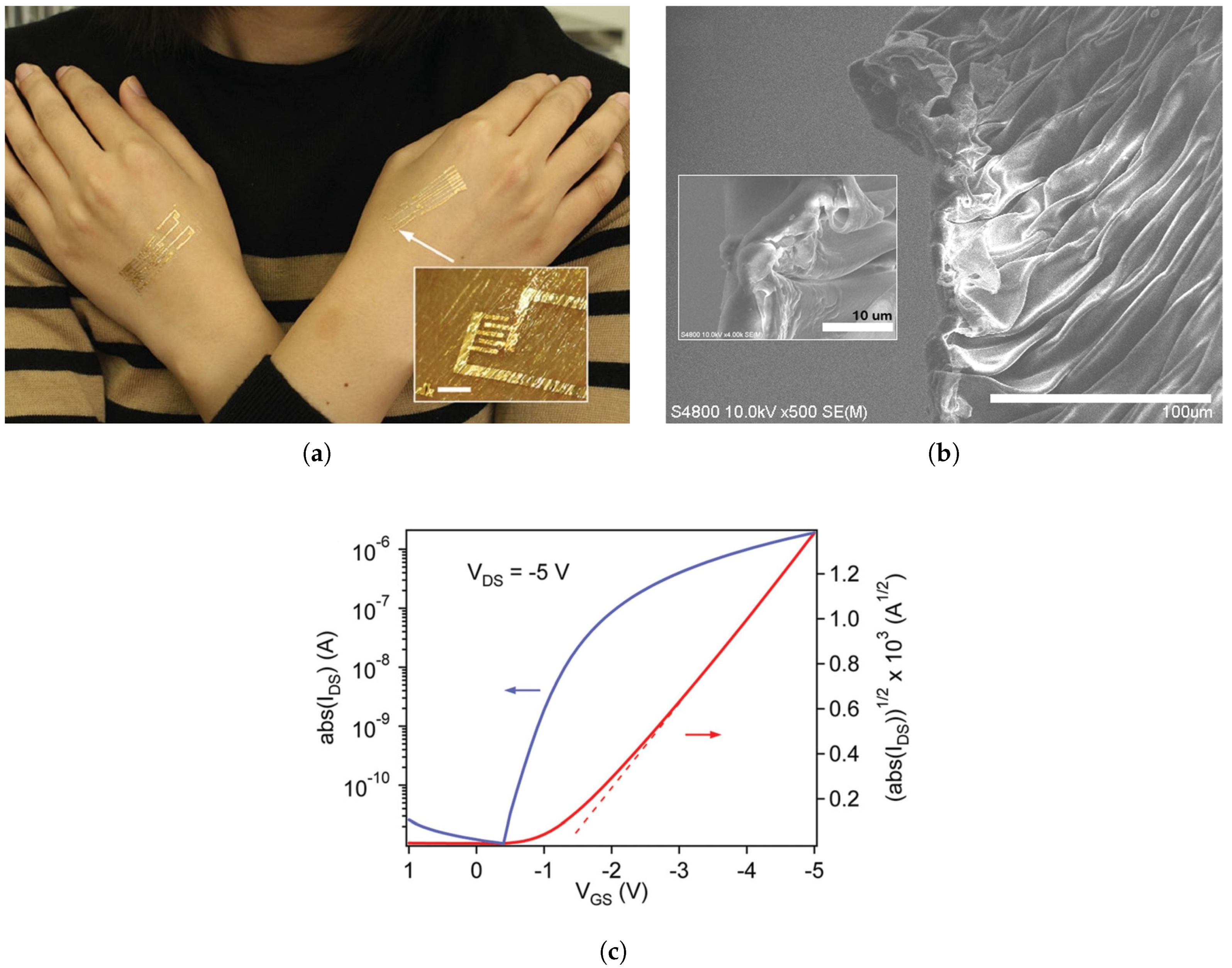
5. Carbon Nanotubes
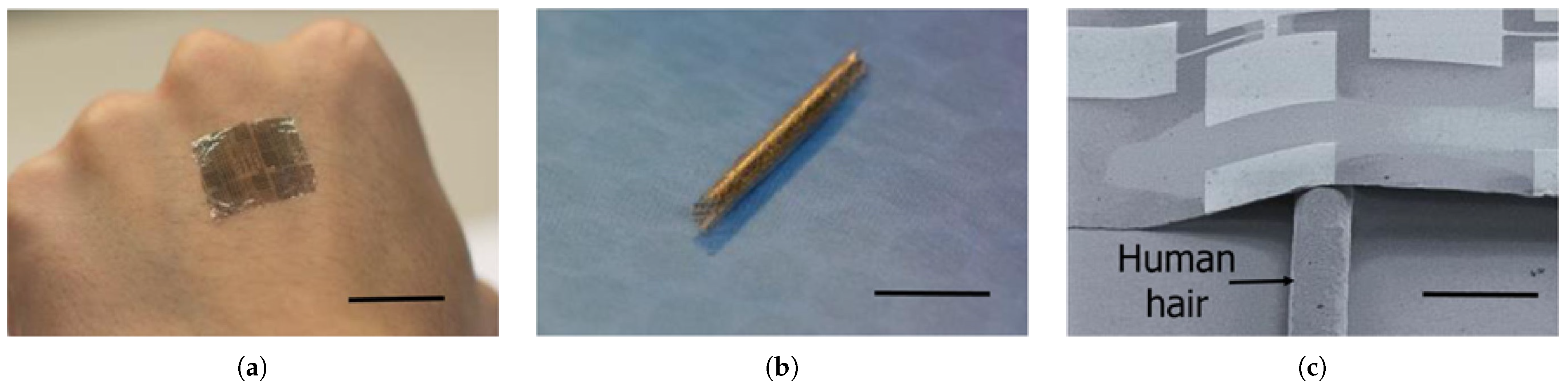
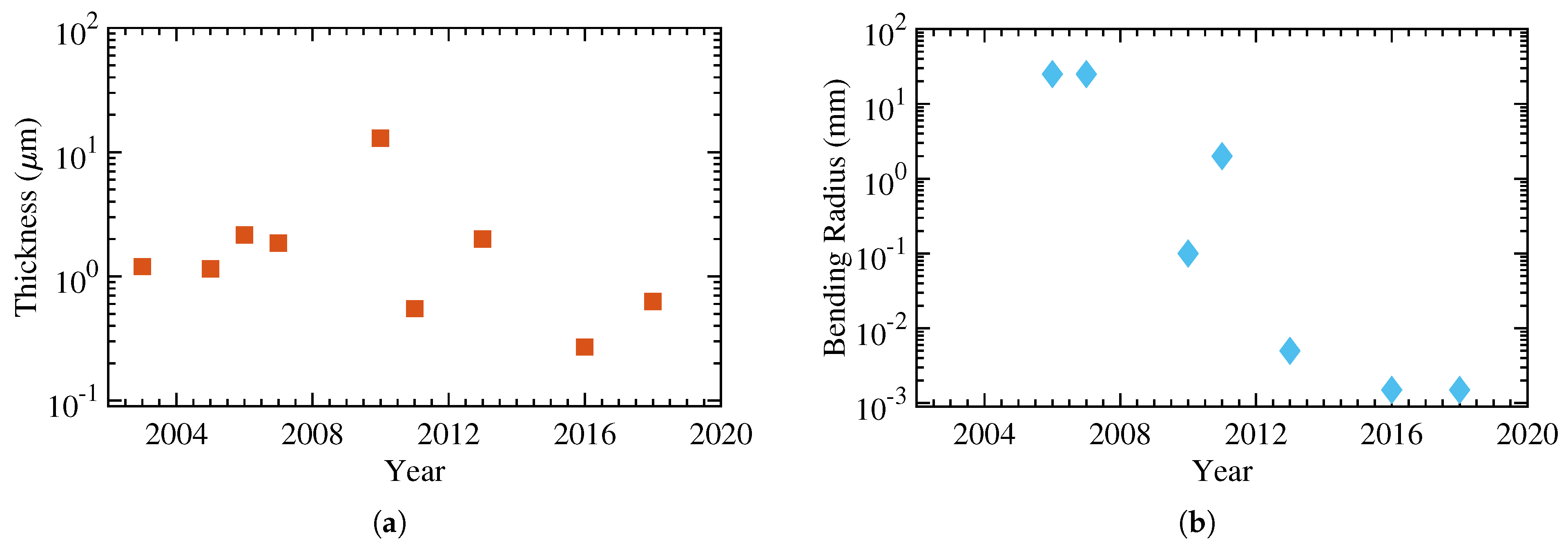
6. Organic Semiconductors
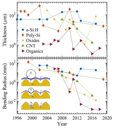
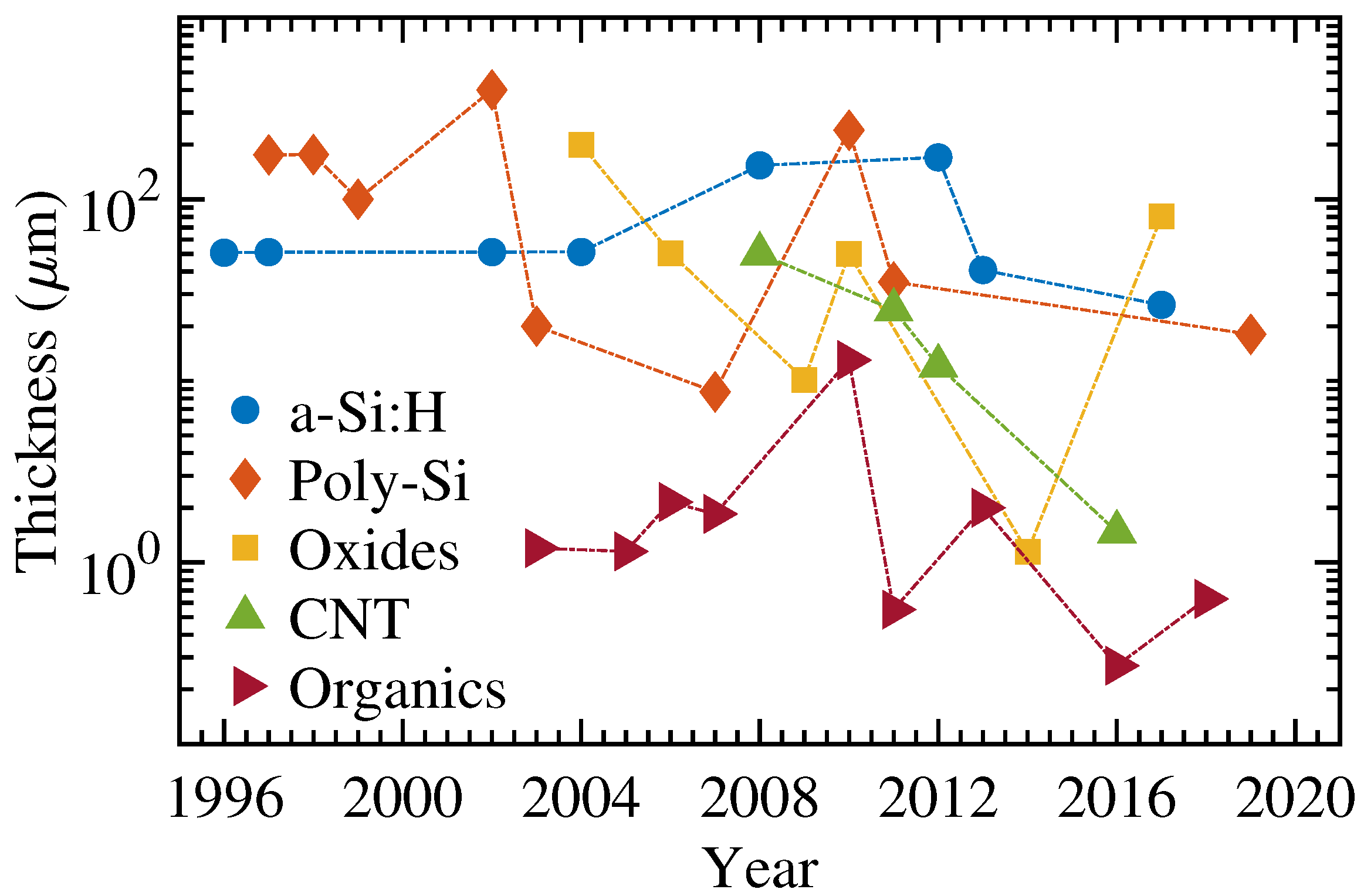
7. Comparison of Semiconducting Technologies
8. Conclusions
Author Contributions
Funding
Acknowledgments
Conflicts of Interest
References
- Nathan, A.; Chalamala, B. Special Issue on Flexible Electronics Technology, Part II: Materials and Devices. Proc. IEEE 2005, 93, 1391–1393. [Google Scholar] [CrossRef]
- Khan, Y.; Garg, M.; Gui, Q.; Schadt, M.; Gaikwad, A.; Han, D.; Yamamoto, N.A.D.; Hart, P.; Welte, R.; Wilson, W.; et al. Flexible Hybrid Electronics: Direct Interfacing of Soft and Hard Electronics for Wearable Health Monitoring. Adv. Funct. Mater. 2016, 26, 8764–8775. [Google Scholar] [CrossRef]
- Pu, X.; Li, L.; Song, H.; Du, C.; Zhao, Z.; Jiang, C.; Cao, G.; Hu, W.; Wang, Z.L. A Self-Charging Power Unit by Integration of a Textile Triboelectric Nanogenerator and a Flexible Lithium-Ion Battery for Wearable Electronics. Adv. Mater. 2015, 27, 2472–2478. [Google Scholar] [CrossRef]
- Zhou, L.; Wanga, A.; Wu, S.C.; Sun, J.; Park, S.; Jackson, T.N. All-organic active matrix flexible display. Appl. Phys. Lett. 2006, 88, 083502. [Google Scholar] [CrossRef]
- Rogers, J.A.; Someya, T.; Huang, Y. Materials and Mechanics for Stretchable Electronics. Science 2010, 327, 1603–1607. [Google Scholar] [CrossRef] [PubMed] [Green Version]
- Sekitani, T.; Kaltenbrunner, M.; Yokota, T.; Someya, T. 11.2: Invited Paper: Imperceptible Electronic Skin. SID Symp. Digest Tech. Pap. 2014, 45, 122–125. [Google Scholar] [CrossRef]
- Sun, Y.; Rogers, J. Inorganic Semiconductors for Flexible Electronics. Adv. Mater. 2007, 19, 1897–1916. [Google Scholar] [CrossRef]
- Lee, J.K.; Lim, Y.S.; Park, C.H.; Park, Y.I.; Kim, C.D.; Hwang, Y.K. a-Si:H Thin-Film Transistor-Driven Flexible Color E-Paper Display on Flexible Substrates. IEEE Electron Device Lett. 2010, 31, 833–835. [Google Scholar] [CrossRef]
- Huang, J.J.; Chen, Y.P.; Huang, Y.S.; Hu, G.R.; Lin, C.W.; Chen, Y.J.; Lee, P.F.; Tsai, C.J.; Liu, C.J.; Yao, H.C.; et al. 58.1: A 4.1-Inch Flexible QVGA AMOLED Using a Microcrystalline-Si:H TFT on a Polyimide Substrate. SID Symp. Digest Tech. Pap. 2009, 40, 866–869. [Google Scholar] [CrossRef]
- Ito, M.; Kon, M.; Ishizaki, M.; Sekine, N. A flexible active-matrix TFT array with amorphous oxide semiconductors for electronic paper. In Proceedings of the 12th International Display Workshops in Conjunction with Asia Display, IDW/AD’05, Takamatsu, Japan, 6–9 December 2005; pp. 845–846. [Google Scholar]
- Chen, Y.; Au, J.; Kazlas, P.; Ritenour, A.; Gates, H.; Mccreary, M. Flexible active-matrix electronic ink display. Nature 2003, 423, 136. [Google Scholar] [CrossRef]
- Rogers, J.A.; Bao, Z.; Baldwin, K.; Dodabalapur, A.; Crone, B.; Raju, V.R.; Kuck, V.; Katz, H.; Amundson, K.; Ewing, J.; et al. Paper-like electronic displays: Large-area rubber-stamped plastic sheets of electronics and microencapsulated electrophoretic inks. Proc. Natl. Acad. Sci. USA 2001, 98, 4835–4840. [Google Scholar] [CrossRef] [PubMed] [Green Version]
- Petti, L.; Münzenrieder, N.; Vogt, C.; Faber, H.; Büthe, L.; Cantarella, G.; Bottacchi, F.; Anthopoulos, T.D.; Tröster, G. Metal oxide semiconductor thin-film transistors for flexible electronics. Appl. Phys. Rev. 2016, 3, 021303. [Google Scholar] [CrossRef] [Green Version]
- Liu, H.; Jian, R.; Chen, H.; Tian, X.; Sun, C.; Zhu, J.; Yang, Z.; Sun, J.; Wang, C. Application of Biodegradable and Biocompatible Nanocomposites in Electronics: Current Status and Future Directions. Nanomaterials 2019, 9, 950. [Google Scholar] [CrossRef] [PubMed] [Green Version]
- Oh, J.Y.; Rondeau-Gagné, S.; Chiu, Y.C.; Chortos, A.; Lissel, F.; Wang, G.J.N.; Schroeder, B.C.; Kurosawa, T.; Lopez, J.; Katsumata, T.; et al. Intrinsically stretchable and healable semiconducting polymer for organic transistors. Nature 2016, 539, 411–415. [Google Scholar] [CrossRef] [PubMed]
- Kaltenbrunner, M.; Sekitani, T.; Reeder, J.; Yokota, T.; Kuribara, K.; Tokuhara, T.; Drack, M.; Schwödiauer, R.; Graz, I.; Bauer-Gogonea, S.; et al. An ultra-lightweight design for imperceptible plastic electronics. Nature 2013, 499, 458–463. [Google Scholar] [CrossRef] [PubMed]
- Nawrocki, R.A. Super- and Ultrathin Organic Field-Effect Transistors: from Flexibility to Super- and Ultraflexibility. Adv. Funct. Mater. 2019, 29, 1906908. [Google Scholar] [CrossRef]
- Baran, D.; Corzo, D.; Blazquez, G. Flexible Electronics: Status, Challenges and Opportunities. Front. Electron. 2020, 1, 2. [Google Scholar] [CrossRef]
- Nawrocki, R.A.; Jin, H.; Lee, S.; Yokota, T.; Sekino, M.; Someya, T. Self-Adhesive and Ultra-Conformable, Sub-300 nm Dry Thin-Film Electrodes for Surface Monitoring of Biopotentials. Adv. Funct. Mater. 2018, 28, 1803279. [Google Scholar] [CrossRef]
- Bock, K. Polymer Electronics Systems - Polytronics. Proc. IEEE 2005, 93, 1400–1406. [Google Scholar] [CrossRef]
- Allen, K. Reel to Real: Prospects for Flexible Displays. Proc. IEEE 2005, 93, 1394–1399. [Google Scholar] [CrossRef]
- Xu, H.; Luo, D.; Li, M.; Xu, M.; Zou, J.; Tao, H.; Lan, L.; Wang, L.; Peng, J.; Cao, Y. A flexible AMOLED display on the PEN substrate driven by oxide thin-film transistors using anodized aluminium oxide as dielectric. J. Mater. Chem. C 2014, 2, 1255–1259. [Google Scholar] [CrossRef]
- Nathan, A.; Chalamala, B. Special Issue on Flexible Electronics Technology, Part 1: Systems and Applications. Proc. IEEE 2005, 93, 1235–1238. [Google Scholar] [CrossRef]
- Münzenrieder, N.; Petti, L.; Zysset, C.; Kinkeldei, T.; Salvatore, G.A.; Tröster, G. Flexible Self-Aligned Amorphous InGaZnO Thin-Film Transistors With Submicrometer Channel Length and a Transit Frequency of 135 MHz. IEEE Trans. Electron Devices 2013, 60, 2815–2820. [Google Scholar] [CrossRef]
- Cherenack, K.H.; Kattamis, A.Z.; Hekmatshoar, B.; Sturm, J.C.; Wagner, S. Amorphous-Silicon Thin-Film Transistors Fabricated at 300 ∘C on a Free-Standing Foil Substrate of Clear Plastic. IEEE Electron Device Lett. 2007, 28, 1004–1006. [Google Scholar] [CrossRef]
- Yang, C.S.; Smith, L.L.; Arthur, C.B.; Parsons, G.N. Stability of low-temperature amorphous silicon thin film transistors formed on glass and transparent plastic substrates. J. Vacuum Sci. Technol. B Microelectron. Nanometer Struct. Process. Meas. Phenomena 2000, 18, 683–689. [Google Scholar] [CrossRef]
- Shim, G.W.; Hong, W.; Cha, J.H.; Park, J.H.; Lee, K.J.; Choi, S.Y. TFT Channel Materials for Display Applications: From Amorphous Silicon to Transition Metal Dichalcogenides. Adv. Mater. 2020, 32, 1907166. [Google Scholar] [CrossRef] [PubMed]
- Chang, T.C.; Tsao, Y.C.; Chen, P.H.; Tai, M.C.; Huang, S.P.; Su, W.C.; Chen, G.F. Flexible low-temperature polycrystalline silicon thin-film transistors. Mater. Today Adv. 2020, 5, 100040. [Google Scholar] [CrossRef]
- Jeong, J.K. The status and perspectives of metal oxide thin-film transistors for active matrix flexible displays. Semicond. Sci. Technol. 2011, 26, 034008. [Google Scholar] [CrossRef]
- Kamiya, T.; Nomura, K.; Hosono, H. Present status of amorphous In–Ga–Zn–O thin-film transistors. Sci. Technol. Adv. Mater. 2010, 11, 044305. [Google Scholar] [CrossRef] [PubMed]
- De la Fuente Vornbrock, A.; Almanza-Workman, M.; Dickin, F.; Elder, R.E.; Garcia, R.A.; Holland, E.; Jackson, W.; Jam, M.; Jeans, A.; Kim, H.J.; et al. A comparison of processes and challenges between organic, a-Si:H, and oxide TFTs for active matrix backplanes on plastic. In Proceedings of the 2012 19th International Workshop on Active-Matrix Flatpanel Displays and Devices (AM-FPD), Kyoto, Japan, 4–6 July 2012; pp. 57–60. [Google Scholar]
- Che, Y.; Chen, H.; Gui, H.; Liu, J.; Liu, B.; Zhou, C. Review of carbon nanotube nanoelectronics and macroelectronics. Semicond. Sci. Technol. 2014, 29, 073001. [Google Scholar] [CrossRef]
- Wang, C.; Takei, K.; Takahashi, T.; Javey, A. Carbon nanotube electronics—Moving forward. Chem. Soc. Rev. 2013, 42, 2592–2609. [Google Scholar] [CrossRef]
- Liu, B.; Wang, C.; Liu, J.; Che, Y.; Zhou, C. Aligned carbon nanotubes: from controlled synthesis to electronic applications. Nanoscale 2013, 5, 9483–9502. [Google Scholar] [CrossRef]
- Kumar, B.; Kaushik, B.K.; Negi, Y.S. Organic Thin Film Transistors: Structures, Models, Materials, Fabrication, and Applications: A Review. Polym. Rev. 2014, 54, 33–111. [Google Scholar] [CrossRef]
- Paterson, A.F.; Singh, S.; Fallon, K.J.; Hodsden, T.; Han, Y.; Schroeder, B.C.; Bronstein, H.; Heeney, M.; McCulloch, I.; Anthopoulos, T.D. Recent Progress in High-Mobility Organic Transistors: A Reality Check. Adv. Mater. 2018, 30, 1801079. [Google Scholar] [CrossRef]
- Okaniwa, H.; Nakatani, K.; Asano, M.; Suzuki, K.; Yano, M.; Hirasaka, M.; Hamakawa, Y. Hydrogenated amorphous silicon solar cell on organic polymer substrate. IEICE Trans. (1976–1990) 1983, 66, 34–38. [Google Scholar]
- Tsukada, T. Amorphous silicon thin-film transistors. J. Non-Cryst. Solids 1993, 164-166, 721–726. [Google Scholar] [CrossRef]
- Long, K.; Kattamis, A.; Cheng, I.C.; Gleskova, H.; Wagner, S.; Sturm, J. Stability of amorphous-silicon TFTs deposited on clear plastic substrates at 250/spl deg/C to 280/spl deg/C. IEEE Electron Device Lett. 2006, 27, 111–113. [Google Scholar] [CrossRef]
- Street, R.A. Trapping parameters of dangling bonds in hydrogenated amorphous silicon. Appl. Phys. Lett. 1982, 41, 1060–1062. [Google Scholar] [CrossRef]
- Feenstra, K.F.; Schropp, R.E.I.; Van der Weg, W.F. Deposition of amorphous silicon films by hot-wire chemical vapor deposition. J. Appl. Phys. 1999, 85, 6843–6852. [Google Scholar] [CrossRef]
- Schropp, R. Industrialization of Hot Wire Chemical Vapor Deposition for thin film applications. Thin Solid Films 2015, 595, 272–283. [Google Scholar] [CrossRef] [Green Version]
- Street, R.A. Thin-Film Transistors. Adv. Mater. 2009, 21, 2007–2022. [Google Scholar] [CrossRef]
- Kuo, Y. Thin Film Transistor Technology–Past, Present, and Future. Interface Mag. 2013, 22, 55–61. [Google Scholar] [CrossRef]
- Van Berkel, C.; Powell, M.J. Resolution of amorphous silicon thin-film transistor instability mechanisms using ambipolar transistors. Appl. Phys. Lett. 1987, 51, 1094–1096. [Google Scholar] [CrossRef]
- Wen, Y.; Liu, Y.; Guo, Y.; Yu, G.; Hu, W. Experimental Techniques for the Fabrication and Characterization of Organic Thin Films for Field-Effect Transistors. Chem. Rev. 2011, 111, 3358–3406. [Google Scholar] [CrossRef] [PubMed]
- Gleskova, H.; Konenkamp, R.; Wagner, S. Electrophotographically patterned thin-film silicon transistors. IEEE Electron Device Lett. 1996, 17, 264–266. [Google Scholar] [CrossRef]
- Gleskova, H.; Wagner, S.; Zhang, Q.; Shen, D.S. Via hole technology for thin-film transistor circuits. IEEE Electron Device Lett. 1997, 18, 523–525. [Google Scholar] [CrossRef]
- Hsu, P.I.; Gleskova, H.; Huang, M.; Suo, Z.; Wagner, S.; Sturm, J.C. Amorphous Si TFTs on plastically deformed spherical domes. J. Non-Cryst. Solids 2002, 299-302, 1355–1359. [Google Scholar] [CrossRef]
- Hsu, P.H.I.; Member, S.; Huang, M.; Gleskova, H.; Xi, Z.; Suo, Z.; Wagner, S.; Sturm, J.C. Effects of Mechanical Strain on TFTs on Spherical Domes. IEEE Trans. Electron Devices 2004, 51, 371–377. [Google Scholar] [CrossRef]
- Kim, S.H.; Cheon, J.H.; Kim, E.B.; Bae, J.H.; Hur, J.H.; Jang, J. High-performance hydrogenated amorphous silicon TFT on flexible metal foil with polyimide planarization. J. Non-Cryst. Solids 2008, 354, 2529–2533. [Google Scholar] [CrossRef]
- Hoehla, S.; Garner, S.; Hohmann, M.; Kuhls, O.; Li, X.; Schindler, A.; Fruehauf, N. Active matrix color-LCD on 75 μm thick flexible glass substrates. IEEE/OSA J. Disp. Technol. 2012, 8, 309–316. [Google Scholar] [CrossRef]
- Huang, J.J.; Chen, C.N. Effect of electrical and mechanical stresses of low temperature a-Si:H thin film transistors fabricated on polyimide and glass substrates. Thin Solid Films 2013, 529, 454–458. [Google Scholar] [CrossRef]
- Kim, M.; Oh, H.; Park, S.; Cho, K.; Kim, S. Mechanical strain-induced defect states in amorphous silicon channel layers of thin-film transistors. Thin Solid Films 2017, 641, 43–46. [Google Scholar] [CrossRef]
- Kallel, S.; Semmache, B.; Lemiti, M.; Dubois, C.; Jaffrezic, H.; Laugier, A. Growth and physical properties of in situ phosphorus-doped RTLPCVD polycrystalline silicon thin films. Mater. Sci. Semicond. Process. 1998, 1, 299–302. [Google Scholar] [CrossRef]
- Hatalis, M.; Greve, D. High-performance thin-film transistors in low-temperature crystallized LPCVD amorphous silicon films. IEEE Electron Device Lett. 1987, 8, 361–364. [Google Scholar] [CrossRef]
- Sameshima, T.; Usui, S.; Sekiya, M. XeCl Excimer laser annealing used in the fabrication of poly-Si TFT’s. IEEE Electron Device Lett. 1986, 7, 276–278. [Google Scholar] [CrossRef]
- Matsuo, N.; Heya, A.; Hamada, H. Review—Technology Trends of Poly-Si TFTs from the Viewpoints of Crystallization and Device Performance. ECS J. Solid State Sci. Technol. 2019, 8, P239–P252. [Google Scholar] [CrossRef]
- Brotherton, S.D. Polycrystalline silicon thin film transistors. Semicond. Sci. Technol. 1995, 10, 721–738. [Google Scholar] [CrossRef]
- Yoshikawa, T.; Yagi, T.; Oka, N.; Jia, J.; Yamashita, Y.; Hattori, K.; Seino, Y.; Taketoshi, N.; Baba, T.; Shigesato, Y. Thermal conductivity of amorphous indium–gallium–zinc oxide thin films. Appl. Phys. Express 2013, 6, 021101. [Google Scholar] [CrossRef]
- Tai, Y.C.; Mastrangelo, C.H.; Muller, R.S. Thermal conductivity of heavily doped low-pressure chemical vapor deposited polycrystalline silicon films. J. Appl. Phys. 1988, 63, 1442–1447. [Google Scholar] [CrossRef]
- Herlogsson, L. Electrolyte-Gated Organic Thin-Film Transistors. Ph.D. Thesis, Linköping University Electronic Press, Linköping, Sweden, 2011. [Google Scholar]
- Smith, P.M.; Carey, P.G.; Sigmon, T.W. Excimer laser crystallization and doping of silicon films on plastic substrates. Appl. Phys. Lett. 1997, 70, 342–344. [Google Scholar] [CrossRef]
- Theiss, S.; Carey, P.; Smith, P.; Wickboldt, P.; Sigmon, T.; Tung, Y.; King, T.J. Polysilicon thin film transistors fabricated at 100/spl deg/C on a flexible plastic substrate. In Proceedings of the International Electron Devices Meeting 1998. Technical Digest (Cat. No. 98CH36217), San Francisco, CA, USA, 6–9 December 1998; pp. 257–260. [Google Scholar] [CrossRef]
- Serikawa, T.; Omata, F. High-mobility poly-Si TFT’s fabricated on flexible stainless-steel substrates. IEEE Electron Device Lett. 1999, 20, 574–576. [Google Scholar] [CrossRef]
- Inoue, S.; Utsunomiya, S.; Saeki, T.; Shimoda, T. Surface-free technology by laser annealing (SUFTLA) and its application to poly-Si TFT-LCDs on plastic film with integrated drivers. IEEE Trans. Electron Devices 2002, 49, 1353–1360. [Google Scholar] [CrossRef]
- Lee, Y.; Li, H.; Fonash, S.J. High-performance poly-Si TFT on plastic substrates using a nano-structured separation layer approach. IEEE Electron Device Lett. 2003, 24, 19–21. [Google Scholar] [CrossRef]
- Pecora, A.; Maiolo, L.; Cuscuna, M.; Simeone, D.; Minotti, A.; Mariucci, L.; Fortunato, G. Polysilicon Thin Film Transistors on spin-coated Polyimide layer for flexible electronics. In Korea Information Display Society: Proceedings of the Conference; The Korean Information Display Society: Seoul, Korea, 2007; pp. 261–264. [Google Scholar]
- An, S.; Lee, J.; Kim, Y.; Kim, T.; Jin, D.; Min, H.; Chung, H.; Kim, S.S. 47.2: 2.8-Inch WQVGA flexible AMOLED using high performance low temperature polysilicon TFT on plastic substrates. In 48th Annual SID Symposium, Seminar, and Exhibition 2010, Display Week 2010; Blackwell Publishing Ltd.: Oxford, UK, 2010; Volume 41, pp. 706–709. [Google Scholar]
- Zampetti, E.; Maiolo, L.; Pecora, A.; Maita, F.; Pantalei, S.; Minotti, A.; Valletta, A.; Cuscun, M.; MacAgnano, A.; Fortunato, G.; et al. Flexible sensorial system based on capacitive chemical sensors integrated with readout circuits fully fabricated on ultra thin substrate. Sens. Actuators B Chem. 2011, 155, 768–774. [Google Scholar] [CrossRef]
- Park, C.B. Investigation of the electromechanical stability of low temperature polycrystalline silicon thin-film transistors governed by types of stress. Solid-State Electron. 2019, 160, 107616. [Google Scholar] [CrossRef]
- Nomura, K.; Ohta, H.; Ueda, K.; Kamiya, T.; Hirano, M.; Hosono, H. Thin-Film Transistor Fabricated in Single-Crystalline Transparent Oxide Semiconductor. Science 2003, 300, 1269–1272. [Google Scholar] [CrossRef] [PubMed]
- Nomura, K.; Ohta, H.; Takagi, A.; Kamiya, T.; Hirano, M.; Hosono, H. Room-temperature fabrication of transparent flexible thin-film transistors using amorphous oxide semiconductors. Nature 2004, 432, 488–492. [Google Scholar] [CrossRef]
- He, Y.; Wang, X.; Gao, Y.; Hou, Y.; Wan, Q. Oxide-based thin film transistors for flexible electronics. J. Semicond. 2018, 39, 011005. [Google Scholar] [CrossRef]
- Fortunato, E.; Barquinha, P.; Martins, R. Oxide Semiconductor Thin-Film Transistors: A Review of Recent Advances. Adv. Mater. 2012, 24, 2945–2986. [Google Scholar] [CrossRef]
- Zhang, Y.H.; Mei, Z.X.; Liang, H.L.; Du, X.L. Review of flexible and transparent thin-film transistors based on zinc oxide and related materials. Chin. Phys. B 2017, 26, 047307. [Google Scholar] [CrossRef] [Green Version]
- Zeumault, A.; Ma, S.; Holbery, J. Fully inkjet-printed metal-oxide thin-film transistors on plastic. Phys. Status Solidi (a) 2016, 213, 2189–2195. [Google Scholar] [CrossRef]
- Jo, J.W.; Kim, J.; Kim, K.T.; Kang, J.G.; Kim, M.G.; Kim, K.H.; Ko, H.; Kim, Y.H.; Park, S.K. Highly Stable and Imperceptible Electronics Utilizing Photoactivated Heterogeneous Sol-Gel Metal–Oxide Dielectrics and Semiconductors. Adv. Mater. 2015, 27, 1182–1188. [Google Scholar] [CrossRef]
- Liu, J.; Buchholz, D.B.; Chang, R.P.H.; Facchetti, A.; Marks, T. High-performance flexible transparent thin-film transistors using a hybrid gate dielectric and an amorphous zinc indium tin oxide channel. J. Adv. Mater. 2010, 22, 2333–2337. [Google Scholar] [CrossRef]
- Nag, M.; Bhoolokam, A.; Smout, S.; Willegems, M.; Muller, R.; Myny, K.; Schols, S.; Ameys, M.; Genoe, J.; Ke, T.H.; et al. Circuits and AMOLED display with self-aligned a-IGZO TFTs on polyimide foil. J. Soc. Inf. Disp. 2014, 22, 509–517. [Google Scholar] [CrossRef]
- Ito, M.; Kon, M.; Miyazaki, C.; Ikeda, N.; Ishizaki, M.; Matsubara, R.; Ugajin, Y.; Sekine, N. Amorphous oxide TFT and their applications in electrophoretic displays. Phys. Status Solidi (a) 2008, 205, 1885–1894. [Google Scholar] [CrossRef]
- Li, X.; Jang, J. Stretchable oxide TFT for wearable electronics. Inf. Disp. 2017, 33, 12–39. [Google Scholar] [CrossRef] [Green Version]
- Jung, S.W.; Koo, J.B.; Park, C.W.; Na, B.S.; Oh, J.Y.; Lee, S.S.; Koo, K.W. Flexible nonvolatile memory transistors using indium gallium zinc oxide-channel and ferroelectric polymer poly(vinylidene fluoride-co-trifluoroethylene) fabricated on elastomer substrate. J. Vacuum Sci. Technol. B 2015, 33, 051201. [Google Scholar] [CrossRef]
- Kim, S.J.; Jeon, D.B.; Park, J.H.; Ryu, M.K.; Yang, J.H.; Hwang, C.S.; Kim, G.H.; Yoon, S.M. Nonvolatile Memory Thin-Film Transistors Using Biodegradable Chicken Albumen Gate Insulator and Oxide Semiconductor Channel on Eco-Friendly Paper Substrate. ACS Appl. Mater. Interfaces 2015, 7, 4869–4874. [Google Scholar] [CrossRef]
- Wang, Z.; Alshammari, F.H.; Omran, H.; Hota, M.K.; Al-Jawhari, H.A.; Salama, K.N.; Alshareef, H.N. All-Oxide Thin Film Transistors and Rectifiers Enabling On-Chip Capacitive Energy Storage. Adv. Electron. Mater. 2019, 5, 1900531. [Google Scholar] [CrossRef]
- Choi, J.Y.; Lee, S.Y. Comprehensive review on the development of high mobility in oxide thin film transistors. J. Korean Phys. Soc. 2017, 71, 516–527. [Google Scholar] [CrossRef]
- Song, J.; Huang, X.; Han, C.; Yu, Y.; Su, Y.; Lai, P. Recent Developments of Flexible InGaZnO Thin-Film Transistors. Phys. Status Solidi (a) 2021, 218, 2000527. [Google Scholar] [CrossRef]
- Jung, S.W.; Choi, J.S.; Park, J.H.; Koo, J.B.; Park, C.W.; Na, B.S.; Oh, J.Y.; Lim, S.C.; Lee, S.S.; Chu, H.Y.; et al. Oxide Semiconductor-Based Flexible Organic/Inorganic Hybrid Thin-Film Transistors Fabricated on Polydimethylsiloxane Elastomer. J. Nanosci. Nanotechnol. 2016, 16, 2752–2755. [Google Scholar] [CrossRef]
- Erb, R.M.; Cherenack, K.H.; Stahel, R.E.; Libanori, R.; Kinkeldei, T.; Münzenrieder, N.; Tröster, G.; Studart, A.R. Locally Reinforced Polymer-Based Composites for Elastic Electronics. ACS Appl. Mater. Interfaces 2012, 4, 2860–2864. [Google Scholar] [CrossRef]
- Dai, M.K.; Lian, J.T.; Lin, T.Y.; Chen, Y.F. High-performance transparent and flexible inorganic thin film transistors: A facile integration of graphene nanosheets and amorphous InGaZnO. J. Mater. Chem. C 2013, 1, 5064–5071. [Google Scholar] [CrossRef]
- Jackson, W.B.; Herman, G.S.; Hoffman, R.L.; Taussig, C.; Braymen, S.; Jeffery, F.; Hauschildt, J. Zinc tin oxide transistors on flexible substrates. J. Non-Cryst. Solids 2006, 352, 1753–1755. [Google Scholar] [CrossRef]
- Park, J.S.; Kim, T.W.; Stryakhilev, D.; Lee, J.S.; An, S.G.; Pyo, Y.S.; Lee, D.B.; Mo, Y.G.; Jin, D.U.; Chung, H.K. Flexible full color organic light-emitting diode display on polyimide plastic substrate driven by amorphous indium gallium zinc oxide thin-film transistors. Appl. Phys. Lett. 2009, 95, 93–96. [Google Scholar] [CrossRef]
- Song, K.; Noh, J.; Jun, T.; Jung, Y.; Kang, H.Y.; Moon, J. Fully Flexible Solution-Deposited ZnO Thin-Film Transistors. Adv. Mater. 2010, 22, 4308–4312. [Google Scholar] [CrossRef]
- Salvatore, G.A.; Münzenrieder, N.; Kinkeldei, T.; Petti, L.; Zysset, C.; Strebel, I.; Büthe, L.; Tröster, G. Wafer-scale design of lightweight and transparent electronics that wraps around hairs. Nat. Commun. 2014, 5, 2982. [Google Scholar] [CrossRef] [PubMed] [Green Version]
- Cantarella, G.; Vogt, C.; Hopf, R.; Münzenrieder, N.; Andrianakis, P.; Petti, L.; Daus, A.; Knobelspies, S.; Büthe, L.; Tröster, G.; et al. Buckled Thin-Film Transistors and Circuits on Soft Elastomers for Stretchable Electronics. ACS Appl. Mater. Interfaces 2017, 9, 28750–28757. [Google Scholar] [CrossRef]
- Yoon, J.; Bae, G.Y.; Yoo, S.; Yoo, J.I.; You, N.H.; Hong, W.K.; Ko, H.C. Deep-ultraviolet sensing characteristics of transparent and flexible IGZO thin film transistors. J. Alloys Compd. 2020, 817, 152788. [Google Scholar] [CrossRef]
- Martel, R.; Schmidt, T.; Shea, H.R.; Hertel, T.; Avouris, P. Single- and multi-wall carbon nanotube field-effect transistors. Appl. Phys. Lett. 1998, 73, 2447–2449. [Google Scholar] [CrossRef] [Green Version]
- Cui, J.B.; Burghard, M.; Kern, K. Room Temperature Single Electron Transistor by Local Chemical Modification of Carbon Nanotubes. Nano Lett. 2002, 2, 117–120. [Google Scholar] [CrossRef]
- Wu, Z.; Chen, Z.; Du, X.; Logan, J.M.; Sippel, J.; Nikolou, M.; Kamaras, K.; Reynolds, J.R.; Tanner, D.B.; Hebard, A.F.; et al. Transparent, Conductive Carbon Nanotube Films. Science 2004, 305, 1273–1276. [Google Scholar] [CrossRef]
- Kumar, S.; Cola, B.A.; Jackson, R.; Graham, S. A Review of Carbon Nanotube Ensembles as Flexible Electronics and Advanced Packaging Materials. J. Electron. Packag. 2011, 133. [Google Scholar] [CrossRef]
- Avouris, P.; Appenzeller, J.; Martel, R.; Wind, S. Carbon nanotube electronics. Proc. IEEE 2003, 91, 1772–1784. [Google Scholar] [CrossRef]
- Avouris, P. Carbon nanotube electronics. Chem. Phys. 2002, 281, 429–445. [Google Scholar] [CrossRef]
- Hirotani, J.; Ohno, Y. Carbon Nanotube Thin Films for High-Performance Flexible Electronics Applications. Top. Curr. Chem. 2019, 377. [Google Scholar] [CrossRef]
- Wang, H.; Luo, J.; Robertson, A.; Ito, Y.; Yan, W.; Lang, V.; Zaka, M.; Schaffel, F.; Rummeli, M.H.; Briggs, G.A.D.; et al. High-performance field effect transistors from solution processed carbon nanotubes. ACS Nano 2010, 4, 6659–6664. [Google Scholar] [CrossRef] [PubMed]
- Jeong, M.; Lee, K.; Choi, E.; Kim, A.; Lee, S.B. Spray-coated carbon nanotube thin-film transistors with striped transport channels. Nanotechnology 2012, 23, 505203. [Google Scholar] [CrossRef] [PubMed]
- Shimizu, M.; Fujii, S.; Tanaka, T.; Kataura, H. Effects of surfactants on the electronic transport properties of thin-film transistors of single-wall carbon nanotubes. J. Phys. Chem. C 2013, 117, 11744–11749. [Google Scholar] [CrossRef]
- Park, S.; Vosguerichian, M.; Bao, Z. A review of fabrication and applications of carbon nanotube film-based flexible electronics. Nanoscale 2013, 5, 1727–1752. [Google Scholar] [CrossRef] [PubMed]
- Sun, D.M.; Timmermans, M.Y.; Tian, Y.; Nasibulin, A.G.; Kauppinen, E.I.; Kishimoto, S.; Mizutani, T.; Ohno, Y. Flexible high-performance carbon nanotube integrated circuits. Nat. Nanotechnol. 2011, 6, 156–161. [Google Scholar] [CrossRef] [PubMed]
- Kim, J.; Yoo, H.; Ba, V.A.P.; Shin, N.; Hong, S. Dye-functionalized sol-gel matrix on carbon nanotubes for refreshable and flexible gas sensors. Sci. Rep. 2018, 8, 1–8. [Google Scholar] [CrossRef] [PubMed] [Green Version]
- Laurila, T.; Sainio, S.; Caro, M.A. Hybrid carbon based nanomaterials for electrochemical detection of biomolecules. Progress Mater. Sci. 2017, 88, 499–594. [Google Scholar] [CrossRef]
- Yu, Z.; Niu, X.; Liu, Z.; Pei, Q. Intrinsically stretchable polymer light-emitting devices using carbon nanotube-polymer composite electrodes. Adv. Mater. 2011, 23, 3989–3994. [Google Scholar] [CrossRef]
- Feng, C.; Liu, K.; Wu, J.S.; Liu, L.; Cheng, J.S.; Zhang, Y.; Sun, Y.; Li, Q.; Fan, S.; Jiang, K. Flexible, stretchable, transparent conducting films made from superaligned carbon nanotubes. Adv. Funct. Mater. 2010, 20, 885–891. [Google Scholar] [CrossRef]
- Cai, L.; Wang, C. Carbon Nanotube Flexible and Stretchable Electronics. Nanoscale Res. Lett. 2015, 10. [Google Scholar] [CrossRef] [Green Version]
- Cao, Q.; Kim, H.S.; Pimparkar, N.; Kulkarni, J.P.; Wang, C.; Shim, M.; Roy, K.; Alam, M.A.; Rogers, J.A. Medium-scale carbon nanotube thin-film integrated circuits on flexible plastic substrates. Nature 2008, 454, 495–500. [Google Scholar] [CrossRef]
- Takahashi, T.; Takei, K.; Gillies, A.G.; Fearing, R.S.; Javey, A. Carbon nanotube active-matrix backplanes for conformal electronics and sensors. Nano Lett. 2011, 11, 5408–5413. [Google Scholar] [CrossRef]
- Wang, C.; Chien, J.C.; Takei, K.; Takahashi, T.; Nah, J.; Niknejad, A.M.; Javey, A. Extremely bendable, high-performance integrated circuits using semiconducting carbon nanotube networks for digital, analog, and radio-frequency applications. Nano Lett. 2012, 12, 1527–1533. [Google Scholar] [CrossRef]
- Cao, X.; Cao, Y.; Zhou, C. Imperceptible and ultraflexible p-Type transistors and macroelectronics based on carbon nanotubes. ACS Nano 2016, 10, 199–206. [Google Scholar] [CrossRef]
- Tsumura, A.; Koezuka, H.; Ando, T. Macromolecular electronic device: Field-effect transistor with a polythiophene thin film. Appl. Phys. Lett. 1986, 49, 1210–1212. [Google Scholar] [CrossRef]
- Garnier, F.; Hajlaoui, R.; Yassar, A.; Srivastava, P. All-Polymer Field-Effect Transistor Realized by Printing Techniques. Science 1994, 265, 1684–1686. [Google Scholar] [CrossRef] [PubMed]
- Anthony, J.E.; Facchetti, A.; Heeney, M.; Marder, S.R.; Zhan, X. n-Type Organic Semiconductors in Organic Electronics. Adv. Mater. 2010, 22, 3876–3892. [Google Scholar] [CrossRef]
- Sirringhaus, H. Reliability of organic field-effect transistors. Adv. Mater. 2009, 21, 3859–3873. [Google Scholar] [CrossRef]
- Klauk, H.; Zschieschang, U.; Halik, M. Low-voltage organic thin-film transistors with large transconductance. J. Appl. Phys. 2007, 102, 074514. [Google Scholar] [CrossRef] [Green Version]
- Raval, H.N.; Tiwari, S.P.; Navan, R.R.; Mhaisalkar, S.G.; Rao, V.R. Solution-Processed Bootstrapped Organic Inverters Based on P3HT with a High-k Gate Dielectric Material. IEEE Electron Device Lett. 2009, 30, 484–486. [Google Scholar] [CrossRef]
- Puigdollers, J.; Voz, C.; Martin, I.; Orpella, A.; Vetter, M.; Alcubilla, R. Pentacene thin-film transistors on polymeric gate dielectric: device fabrication and electrical characterization. J. Non-Cryst. Solids 2004, 338, 617–621. [Google Scholar] [CrossRef]
- Buga, C.S.; Viana, J.C. A Review on Materials and Technologies for Organic Large-Area Electronics. Adv. Mater. Technol. 2021, 2001016. [Google Scholar] [CrossRef]
- Park, C.B.; Kim, K.M.; Lee, J.E.; Na, H.; Yoo, S.S.; Yang, M.S. Flexible electrophoretic display driven by solution-processed organic TFT with highly stable bending feature. Org. Electron. 2014, 15, 3538–3545. [Google Scholar] [CrossRef]
- Cantatore, E.; Geuns, T.C.T.; Gelinck, G.H.; van Veenendaal, E.; Gruijthuijsen, A.F.A.; Schrijnemakers, L.; Drews, S.; de Leeuw, D.M. A 13.56-MHz RFID System Based on Organic Transponders. IEEE J. Solid-State Circuits 2007, 42, 84–92. [Google Scholar] [CrossRef] [Green Version]
- Briand, D.; Oprea, A.; Courbat, J.; Bârsan, N. Making environmental sensors on plastic foil. Mater. Today 2011, 14, 416–423. [Google Scholar] [CrossRef]
- Takeda, Y.; Hayasaka, K.; Shiwaku, R.; Yokosawa, K.; Shiba, T.; Mamada, M.; Kumaki, D.; Fukuda, K.; Tokito, S. Fabrication of Ultra-Thin Printed Organic TFT CMOS Logic Circuits Optimized for Low-Voltage Wearable Sensor Applications. Sci. Rep. 2016, 6. [Google Scholar] [CrossRef] [PubMed]
- Guerin, M.; Daami, A.; Jacob, S.; Bergeret, E.; Benevent, E.; Pannier, P.; Coppard, R. High-Gain Fully Printed Organic Complementary Circuits on Flexible Plastic Foils. IEEE Trans. Electron Devices 2011, 58, 3587–3593. [Google Scholar] [CrossRef]
- Yokota, T.; Fukuda, K.; Someya, T. Recent Progress of Flexible Image Sensors for Biomedical Applications. Adv. Mater. 2021, 33, 2004416. [Google Scholar] [CrossRef] [PubMed]
- Viola, F.A.; Spanu, A.; Ricci, P.C.; Bonfiglio, A.; Cosseddu, P. Ultrathin, flexible and multimodal tactile sensors based on organic field-effect transistors. Sci. Rep. 2018, 8. [Google Scholar] [CrossRef] [Green Version]
- Lai, S.; Casula, G.; Ricci, P.C.; Cosseddu, P.; Bonfiglio, A. All-Organic, Low Voltage, Transparent and Compliant Organic Field-Effect Transistor Fabricated by Means of Large-Area, Cost-Effective Techniques. Appl. Sci. 2020, 10. [Google Scholar] [CrossRef]
- Lai, S.; Zucca, A.; Cosseddu, P.; Greco, F.; Mattoli, V.; Bonfiglio, A. Ultra-conformable Organic Field-Effect Transistors and circuits for epidermal electronic applications. Org. Electron. 2017, 46, 60–67. [Google Scholar] [CrossRef]
- Bonfiglio, A.; Mameli, F.; Sanna, O. A completely flexible organic transistor obtained by a one-mask photolithographic process. Appl. Phys. Lett. 2003, 82, 3550–3552. [Google Scholar] [CrossRef]
- Santato, C.; Manunza, I.; Bonfiglio, A.; Cicoira, F.; Cosseddu, P.; Zamboni, R.; Muccini, M. Tetracene light-emitting transistors on flexible plastic substrates. Appl. Phys. Lett. 2005, 86, 1–3. [Google Scholar] [CrossRef]
- Cosseddu, P.; Bonfiglio, A. Soft lithography fabrication of all-organic bottom-contact and top-contact field effect transistors. Appl. Phys. Lett. 2006, 88, 1–3. [Google Scholar] [CrossRef]
- Manunza, I.; Bonfiglio, A. Pressure sensing using a completely flexible organic transistor. Biosens. Bioelectron. 2007, 22, 2775–2779. [Google Scholar] [CrossRef]
- Sekitani, T.; Zschieschang, U.; Klauk, H.; Someya, T. Flexible organic transistors and circuits with extreme bending stability. Nat. Mater. 2010, 9, 1015–1022. [Google Scholar] [CrossRef]
- Cosseddu, P.; Piras, A.; Bonfiglio, A. Fully deformable organic thin-film transistors with moderate operation voltage. IEEE Trans. Electron Devices 2011, 58, 3416–3421. [Google Scholar] [CrossRef]
- Nawrocki, R.A.; Matsuhisa, N.; Yokota, T.; Someya, T. 300-nm Imperceptible, Ultraflexible, and Biocompatible e-Skin Fit with Tactile Sensors and Organic Transistors. Adv. Electron. Mater. 2016, 2, 2–5. [Google Scholar] [CrossRef]
- Ji, X.; Zhou, P.; Zhong, L.; Xu, A.; Tsang, A.C.; Chan, P.K. Smart Surgical Catheter for C-Reactive Protein Sensing Based on an Imperceptible Organic Transistor. Adv. Sci. 2018, 5, 1–8. [Google Scholar] [CrossRef]


| Publication Year | Bending Radius (mm) | Total Thickness (m) | ON/OFF Ratio | Channel Width/Length | Mobility (cm/Vs) | Substrate | Substrate Thickness (m) | Dielectric | Reference |
|---|---|---|---|---|---|---|---|---|---|
| 1996 | 65 | 50.75 | 1000/100 | N/A | alkali-free glass foil | 50 | SiN | [47] | |
| 1997 | 65 | 51.15 | 500/150 | 0.41 | alkali-free glass foil | 50 | SiN | [48] | |
| 2002 | 55 | 51.16 | 14/4 | 0.47 | PI | 50 | SiN | [49] | |
| 2004 | 55 | 51.26 | 25/10 | 0.42 | PI | 50 | SiN | [50] | |
| 2008 | 12.5 | 153.7 | 25/5 | 1.47 | stainless steel foil | 150 | SiN | [51] | |
| 2012 | 5 | 75 | 50/10 | 0.4 | glass foil | 75 | SiN | [52] | |
| 2013 | 25 | 40.75 | 80/8 | 0.45 | PI over glass foil | 40 | SiN | [53] | |
| 2017 | 18 | 26.22 | 10/10 | 0.031 | PI | 25 | SiN | [54] |
| Publication Year | Bending Radius (mm) | Total Thickness (m) | ON/OFF Ratio | Channel Width/Length | Mobility (cm/Vs) | Substrate | Substrate Thickness (m) | Dielectric | Reference |
|---|---|---|---|---|---|---|---|---|---|
| 1997 | N/A | 175.6 | >10 | N/A | N/A | Polyester | 175 | SiO | [63] |
| 1998 | N/A | 176.11 | >10 | 100/50 | 60 | PET | 175 | SiO | [64] |
| 1999 | 125 | >100 | N/A | 106 | stainless steel | 100 | SiO | [65] | |
| 2002 | 20 | >400 | N/A | 10/10 | 63 | PES | 400 | SiO | [66] |
| 2003 | N/A | >20 | N/A | 174 | N/A | 20 | SiO | [67] | |
| 2007 | 13 | 8.695 | >10 | N/A | 70 | PI | 8 | SiO | [68] |
| 2010 | 10 | >240 | N/A | 124 | N/A | 240 | SiO | [69] | |
| 2011 | 6 | 35 | N/A | 150/10 | 60 | PI | 10 | SiO | [70] |
| 2019 | 2 | 18.05 | >10 | 5/4 and 10/6 | 80 | PI | 17 | SiO | [71] |
| Publication Year | Bending Radius (mm) | Total Thickness (m) | ON/OFF Ratio | Channel Width/Length | Mobility (cm/Vs) | Substrate | Substrate Thickness (m) | Dielectric | Semiconductor | Reference |
|---|---|---|---|---|---|---|---|---|---|---|
| 2004 | 30 | >200 | 200/50 | 6–9 | PET | 200 | YO | a-IGZO | [73] | |
| 2006 | N/A | 50.56 | 1000/80 | 14 | stainless steel foil-backed PI | 50 | SiON | ZTO | [91] | |
| 2009 | 3 | 10.15 | >10 | N/A | 15.1 | PI | 10 | SiN | a-IGZO | [92] |
| 2010 | 0.2 | >50 | 10 | 1500/120 | PI | 50 | SiO | ZnO | [93] | |
| 2014 | 0.05 | 1.145 | 280/80 | 26 | Parylene | 1 | AlO | a-IGZO | [94] | |
| 2017 | 0.013 | 80.385 | 280/30 | 13.7 | PDMS | 80 | AlO | a-IGZO | [95] |
| Publication Year | Bending Radius (mm) | Total Thickness (m) | ON/OFF Ratio | Channel Width/Length | Mobility (cm/Vs) | Substrate | Substrate Thickness (m) | Dielectric | Reference |
|---|---|---|---|---|---|---|---|---|---|
| 2008 | 5 | >50 | 10 | 5/100 | 80 | PI | 50 | HfO | [114] |
| 2011 | 2 | 24.58 | 10 | 250/3 | 20–30 | PI | 24 | AlO and SiO | [115] |
| 2012 | 1.27 | 12.105 | 400 | 3/4 | 55 | PI | 12 | AlO and SiO | [116] |
| 2016 | 0.04 | 1.476 | 10 | 100/10 | 12.04 | PET | 1.4 | AlO and SiO | [117] |
| Publication Year | Bending Radius (mm) | Total Thickness (m) | ON/OFF Ratio | Channel Width/Length | Mobility (cm/Vs) | Substrate | Substrate Thickness (m) | Dielectric | Semiconductor | Reference |
|---|---|---|---|---|---|---|---|---|---|---|
| 2003 | N/A | 1.2 | >10 | 60,000/20 | 10 | Mylar | 0.9 | Mylar | Pentacene | [135] |
| 2005 | N/A | 1.15 | N/A | 210,000/70 | Mylar | 0.9 | Mylar | Pentacene | [136] | |
| 2006 | 25 | 2.15 | N/A | 5000/25 | N/A | Mylar | 1.9 | Mylar | Pentacene | [137] |
| 2007 | 25 | 1.85 | N/A | 5000/25 | N/A | Mylar | 1.6 | Mylar | Pentacene | [138] |
| 2010 | 0.1 | 13 | and | 500/50 | 0.5 and 0.1 | PI | 12.5 | AlO | Pentacene and F16CuPc | [139] |
| 2011 | 2 | 0.55 | >10 | 5000/5 | , , and | Parylene | 0.4 | Parylene | Pentacene, TIPS, and N1400 | [140] |
| 2013 | 0.005 | 2 | >10 | 500/40 | 3 | PEN | 1.2 | AlO | DNTT | [16] |
| 2016 | 0.0015 | 0.27 | 1000/100 | 0.34 | Parylene | 0.06 | Parylene | DNTT | [141] | |
| 2018 | 0.0015 | 0.63 | >10 | 35 | PAN | 0.18 | AlO | DPh-BBTNDT | [142] |
Publisher’s Note: MDPI stays neutral with regard to jurisdictional claims in published maps and institutional affiliations. |
© 2021 by the authors. Licensee MDPI, Basel, Switzerland. This article is an open access article distributed under the terms and conditions of the Creative Commons Attribution (CC BY) license (https://creativecommons.org/licenses/by/4.0/).
Share and Cite
Mirshojaeian Hosseini, M.J.; Nawrocki, R.A. A Review of the Progress of Thin-Film Transistors and Their Technologies for Flexible Electronics. Micromachines 2021, 12, 655. https://doi.org/10.3390/mi12060655
Mirshojaeian Hosseini MJ, Nawrocki RA. A Review of the Progress of Thin-Film Transistors and Their Technologies for Flexible Electronics. Micromachines. 2021; 12(6):655. https://doi.org/10.3390/mi12060655
Chicago/Turabian StyleMirshojaeian Hosseini, Mohammad Javad, and Robert A. Nawrocki. 2021. "A Review of the Progress of Thin-Film Transistors and Their Technologies for Flexible Electronics" Micromachines 12, no. 6: 655. https://doi.org/10.3390/mi12060655