Next Issue
Volume 12, June
Previous Issue
Volume 12, April


Micromachines, Volume 12, Issue 5 (May 2021) – 120 articles

Cover Story (view full-size image): 
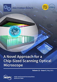
Lensless microscopy has attracted a great deal of attention due to its potential for low-cost microscopy and its use in places where large and expensive equipment is not possible. By changing the role of the detector and emitter in lensless microscopy, a chip-sized scanning optical microscope based only on a fully addressable nano-LED array and an optical photodetector is achieved. Resolution is given by the LED pitch, while field-of-view is given by the scanned area defined by the LED array size. View this paper.
  • Issues are regarded as officially published after their release is announced to the table of contents alert mailing list.
  • You may sign up for e-mail alerts to receive table of contents of newly released issues.
  • PDF is the official format for papers published in both, html and pdf forms. To view the papers in pdf format, click on the "PDF Full-text" link, and use the free Adobe Reader to open them.
Order results
Result details
Section
Select all
Export citation of selected articles as:
10 pages, 2915 KiB  
Communication
A Fiber Ring Laser Sensor with a Side Polished Evanescent Enhanced Fiber for Highly Sensitive Temperature Measurement
by Weihao Lin, Yibin Liu, Liyang Shao and Mang I. Vai
Micromachines 2021, 12(5), 586; https://doi.org/10.3390/mi12050586 - 20 May 2021
Cited by 13 | Viewed by 2349
Abstract
We demonstrate a highly sensitive and practical fiber-based temperature sensor system. The sensor is constructed based on a fiber ring laser (FRL) as well as a side-polished fiber filled with isopropanol. The laser cavity of the sensing part fiber is polished by the [...] Read more.
We demonstrate a highly sensitive and practical fiber-based temperature sensor system. The sensor is constructed based on a fiber ring laser (FRL) as well as a side-polished fiber filled with isopropanol. The laser cavity of the sensing part fiber is polished by the wheel fiber polishing system with residual thickness (RT) is selected to detect the temperature in the FRL. Thanks to the high thermo-optic coefficient of isopropanol, the sensitivity of the proposed temperature sensor could be effectively improved by filling isopropanol in the cost-less side polished single mode fiber. Refractive index (RI) of isopropanol changes with the surrounding temperature variation allowing high-sensitivity temperature sensing. Experimental results demonstrate that the side polished fiber can efficiently excite high-order cladding modes which enhance the modular interference increase the interaction between the evanescent wave and the isopropanol. Besides, the results show that the sensitivity can be as high as 2 nm/°C in the temperature range of 25–35 °C. Full article
(This article belongs to the Special Issue Security and Sensing Devices for Healthcare Technologies)
Show Figures

Figure 1

14 pages, 4645 KiB  
Article
A Microtester for Measuring the Reliability of Microdevices in Controlled Environmental Conditions
by Yunjia Li, Weitao Dou, Chenyuan Zhou, Xinyi Wang, Aijun Yang, Yong Zhang and Dayong Qiao
Micromachines 2021, 12(5), 585; https://doi.org/10.3390/mi12050585 - 20 May 2021
Cited by 3 | Viewed by 2069
Abstract
A miniaturized reliability test system for microdevices with controlled environmental parameters is presented. The system is capable of measuring key electrical parameters of the microdevices while controlling the environmental conditions around the microdevices. The test system is compact and thus can be integrated [...] Read more.
A miniaturized reliability test system for microdevices with controlled environmental parameters is presented. The system is capable of measuring key electrical parameters of the microdevices while controlling the environmental conditions around the microdevices. The test system is compact and thus can be integrated with standard test equipment for microdevices. By using a feed-forward decoupling algorithm, the presented test system is capable of generating a temperature range of 0–120 °C and a humidity range of 20–90% RH (0–55 °C), within a small footprint and weight. The accuracy for temperature and humidity control is ±0.1 °C and ±1% RH (30 °C), respectively. The functionality of the proposed test system is verified by integrating it with a piezo shaker to test the environmental reliability of an electromagnetic vibration energy harvester. The proposed system can be used as a proof-of-technology platform for characterizing the performance of microdevices with controlled environmental parameters. Full article
(This article belongs to the Special Issue Smart Devices and Systems for Vibration Sensing and Energy Harvesting)
Show Figures

Figure 1

10 pages, 2715 KiB  
Article
Novel Program Scheme of Vertical NAND Flash Memory for Reduction of Z-Interference
by Su-in Yi and Jungsik Kim
Micromachines 2021, 12(5), 584; https://doi.org/10.3390/mi12050584 - 20 May 2021
Cited by 10 | Viewed by 3550
Abstract
Minimizing the variation in threshold voltage (Vt) of programmed cells is required to the extreme level for realizing multi-level-cells; as many as even 5 bits per cell recently. In this work, a recent program scheme to write the cells from [...] Read more.
Minimizing the variation in threshold voltage (Vt) of programmed cells is required to the extreme level for realizing multi-level-cells; as many as even 5 bits per cell recently. In this work, a recent program scheme to write the cells from the top, for instance the 170th layer, to the bottom, the 1st layer, (T-B scheme) in vertical NAND (VNAND) Flash Memory, is investigated to minimize Vt variation by reducing Z-interference. With the aid of Technology Computer Aided Design (TCAD) the Z-Interference for T-B (84 mV) is found to be better than B-T (105 mV). Moreover, under scaled cell dimensions (e.g., Lg: 31→24 nm), the improvement becomes protruding (T-B: 126 mV and B-T: 162 mV), emphasizing the significance of the T-B program scheme for the next generation VNAND products with the higher bit density. Full article
(This article belongs to the Special Issue Flash Memory Devices)
Show Figures

Figure 1

16 pages, 10220 KiB  
Article
Morphological Study of Nanostructures Induced by Direct Femtosecond Laser Ablation on Diamond
by Ahmed Abdelmalek, Argyro N. Giakoumaki, Vibhav Bharadwaj, Belén Sotillo, Thien Le Phu, Monica Bollani, Zeyneb Bedrane, Roberta Ramponi, Shane M. Eaton and Malik Maaza
Micromachines 2021, 12(5), 583; https://doi.org/10.3390/mi12050583 - 20 May 2021
Cited by 3 | Viewed by 2879
Abstract
High spatial frequency laser induced periodic surface structure (HSFL) morphology induced by femtosecond laser with 230 fs pulse duration, 250 kHz repetition rate at 1030 nm wavelength on CVD diamond surface is investigated and discussed. The spatial modification was characterized and analyzed by [...] Read more.
High spatial frequency laser induced periodic surface structure (HSFL) morphology induced by femtosecond laser with 230 fs pulse duration, 250 kHz repetition rate at 1030 nm wavelength on CVD diamond surface is investigated and discussed. The spatial modification was characterized and analyzed by Scanning Electron Microscopy (SEM), Atomic Force Microscopy (AFM) and 2D-Fast Fourier Transform (2D-FFT). We studied the effect of pulse number and laser power on the spatial development of nanostructures, and also deduced the impact of thermal accumulation effect on their morphology. A generalized plasmonic model has been used to follow the optical evolution of the irradiated surface and to determine the periodic value of the nanostructures. We suggest that non-thermal melting and plasmonic excitation are the main processes responsible for the formation of HSFL-type nanostructures. Full article
Show Figures

Figure 1

9 pages, 3275 KiB  
Article
A Comparative Study on the Wettability of Unstructured and Structured LiFePO4 with Nanosecond Pulsed Fiber Laser
by Mulugeta Gebrekiros Berhe and Dongkyoung Lee
Micromachines 2021, 12(5), 582; https://doi.org/10.3390/mi12050582 - 20 May 2021
Cited by 12 | Viewed by 2287
Abstract
The wettability of electrodes increases the power and energy densities of the cells of lithium-ion batteries, which is vital to improving their electrochemical performance. Numerous studies in the past have attempted to explain the effect of electrolyte and calendering on wettability. In this [...] Read more.
The wettability of electrodes increases the power and energy densities of the cells of lithium-ion batteries, which is vital to improving their electrochemical performance. Numerous studies in the past have attempted to explain the effect of electrolyte and calendering on wettability. In this work, the wettability behavior of structured and unstructured LiFePO4 electrodes was studied. Firstly, the wettability morphology of the structured electrode was analyzed, and the electrode geometry was quantified in terms of ablation top and bottom width, ablation depth, and aspect ratio. From the result of the geometry analysis, the minimum measured values of aspect ratio and ablation depth were used as structured electrodes. Laser structuring with pitch distances of 112 μm, 224 μm, and 448 μm was applied. Secondly, the wettability of the electrodes was measured mainly by total wetting time and electrolyte spreading area. This study demonstrates that the laser-based structuring of the electrode increases the electrochemically active surface area of the electrode. The electrode structured with 112 μm pitch distance exhibited the fastest wetting at a time of 13.5 s. However, the unstructured electrode exhibited full wetting at a time of 84 s. Full article
Show Figures

Figure 1

19 pages, 5611 KiB  
Article
Numerical Simulation of Effect of Different Initial Morphologies on Melt Hydrodynamics in Laser Polishing of Ti6Al4V
by Kai Li, Zhenyu Zhao, Houming Zhou, Hao Zhou, Jie Yin, Wei Zhang and Guiyao Zhou
Micromachines 2021, 12(5), 581; https://doi.org/10.3390/mi12050581 - 20 May 2021
Cited by 6 | Viewed by 1920
Abstract
As a surface finishing technique for rapid remelting and re-solidification, laser polishing can effectively eliminate the asperities so as to approach the feature size. Nevertheless, the polished surface quality is significantly sensitive to the processing parameters, especially with respect to melt hydrodynamics. In [...] Read more.
As a surface finishing technique for rapid remelting and re-solidification, laser polishing can effectively eliminate the asperities so as to approach the feature size. Nevertheless, the polished surface quality is significantly sensitive to the processing parameters, especially with respect to melt hydrodynamics. In this paper, a transient two-dimensional model was developed to demonstrate the molten flow behavior for different surface morphologies of the Ti6Al4V alloy. It is illustrated that the complex evolution of the melt hydrodynamics involving heat conduction, thermal convection, thermal radiation, melting and solidification during laser polishing. Results show that the uniformity of the distribution of surface peaks and valleys can improve the molten flow stability and obtain better smoothing effect. The high cooling rate of the molten pool resulting in a shortening of the molten lifetime, which prevents the peaks from being removed by capillary and thermocapillary forces. It is revealed that the mechanism of secondary roughness formation on polished surface. Moreover, the double spiral nest Marangoni convection extrudes the molten to the outsides. It results in the formation of expansion and depression, corresponding to nearby the starting position and at the edges of the polished surface. It is further found that the difference between the simulation and experimental depression depths is only about 2 μm. Correspondingly, the errors are approximately 8.3%, 14.3% and 13.3%, corresponding to Models 1, 2 and 3, respectively. The aforementioned results illustrated that the predicted surface profiles agree reasonably well with the experimentally measured surface height data. Full article
(This article belongs to the Special Issue Emerging Micro Manufacturing Technologies and Applications)
Show Figures

Figure 1

14 pages, 4815 KiB  
Article
Room Temperature Direct Electron Beam Lithography in a Condensed Copper Carboxylate
by Luisa Berger, Jakub Jurczyk, Katarzyna Madajska, Iwona B. Szymańska, Patrik Hoffmann and Ivo Utke
Micromachines 2021, 12(5), 580; https://doi.org/10.3390/mi12050580 - 20 May 2021
Cited by 7 | Viewed by 3343
Abstract
High-resolution metallic nanostructures can be fabricated with multistep processes, such as electron beam lithography or ice lithography. The gas-assisted direct-write technique known as focused electron beam induced deposition (FEBID) is more versatile than the other candidates. However, it suffers from low throughput. This [...] Read more.
High-resolution metallic nanostructures can be fabricated with multistep processes, such as electron beam lithography or ice lithography. The gas-assisted direct-write technique known as focused electron beam induced deposition (FEBID) is more versatile than the other candidates. However, it suffers from low throughput. This work presents the combined approach of FEBID and the above-mentioned lithography techniques: direct electron beam lithography (D-EBL). A low-volatility copper precursor is locally condensed onto a room temperature substrate and acts as a positive tone resist. A focused electron beam then directly irradiates the desired patterns, leading to local molecule dissociation. By rinsing or sublimation, the non-irradiated precursor is removed, leaving copper-containing structures. Deposits were formed with drastically enhanced growth rates than FEBID, and their composition was found to be comparable to gas-assisted FEBID structures. The influence of electron scattering within the substrate as well as implementing a post-purification protocol were studied. The latter led to the agglomeration of high-purity copper crystals. We present this as a new approach to electron beam-induced fabrication of metallic nanostructures without the need for cryogenic or hot substrates. D-EBL promises fast and easy fabrication results. Full article
(This article belongs to the Special Issue Nanofabrication with Focused Electron/Ion Beam Induced Processing)
Show Figures

Figure 1

10 pages, 4462 KiB  
Article
3D-Printed Micro-Tweezers with a Compliant Mechanism Designed Using Topology Optimization
by Yukihito Moritoki, Taichi Furukawa, Jinyi Sun, Minoru Yokoyama, Tomoyuki Shimono, Takayuki Yamada, Shinji Nishiwaki, Tatsuto Kageyama, Junji Fukuda, Masaru Mukai and Shoji Maruo
Micromachines 2021, 12(5), 579; https://doi.org/10.3390/mi12050579 - 19 May 2021
Cited by 13 | Viewed by 4383
Abstract
The development of handling technology for microscopic biological samples such as cells and spheroids has been required for the advancement of regenerative medicine and tissue engineering. In this study, we developed micro-tweezers with a compliant mechanism to manipulate organoids. The proposed method combines [...] Read more.
The development of handling technology for microscopic biological samples such as cells and spheroids has been required for the advancement of regenerative medicine and tissue engineering. In this study, we developed micro-tweezers with a compliant mechanism to manipulate organoids. The proposed method combines high-resolution microstereolithography that uses a blue laser and topology optimization for shape optimization of micro-tweezers. An actuation system was constructed using a linear motor stage with a force control system to operate the micro-tweezers. The deformation of the topology-optimized micro-tweezers was examined analytically and experimentally. The results verified that the displacement of the tweezer tip was proportional to the applied load; furthermore, the displacement was sufficient to grasp biological samples with an approximate diameter of several hundred micrometers. We experimentally demonstrated the manipulation of an organoid with a diameter of approximately 360 µm using the proposed micro-tweezers. Thus, combining microstereolithography and topology optimization to fabricate micro-tweezers can be potentially used in modifying tools capable of handling various biological samples. Full article
Show Figures

Figure 1

12 pages, 2993 KiB  
Article
Design of Driving Waveform for Shortening Red Particles Response Time in Three-Color Electrophoretic Displays
by Wenjun Zeng, Zichuan Yi, Xichen Zhou, Yiming Zhao, Haoqiang Feng, Jianjun Yang, Liming Liu, Feng Chi, Chongfu Zhang and Guofu Zhou
Micromachines 2021, 12(5), 578; https://doi.org/10.3390/mi12050578 - 19 May 2021
Cited by 11 | Viewed by 2447
Abstract
Three-color electrophoretic displays (EPDs) have the advantages of multi-color display and low power consumption. However, their red particles have the disadvantage of long response time. In this paper, a driving waveform, which is based on electrophoresis theory and reference gray scale optimization, was [...] Read more.
Three-color electrophoretic displays (EPDs) have the advantages of multi-color display and low power consumption. However, their red particles have the disadvantage of long response time. In this paper, a driving waveform, which is based on electrophoresis theory and reference gray scale optimization, was proposed to shorten the response time of red particles in three-color EPDs. The driving waveform was composed of erasing stage, reference gray scale forming stage, red driving stage, and white or black driving stage. Firstly, the characteristics of particle motion were analyzed by electrophoresis theory and Stokes law. Secondly, the reference gray scale of the driving waveform was optimized to shorten the distance between red particles and a common electrode plate. Finally, an experimental platform was developed to test the performance of the driving waveform. Experimental results showed that the proposed driving waveform can shorten the response time of red particles by 65.57% and reduce the number of flickers by 66.67% compared with the traditional driving waveform. Full article
Show Figures

Figure 1

20 pages, 5397 KiB  
Review
Plasmon Induced Photocatalysts for Light-Driven Nanomotors
by Enrique Contreras, Christian Palacios, I. Brian Becerril-Castro and José M. Romo-Herrera
Micromachines 2021, 12(5), 577; https://doi.org/10.3390/mi12050577 - 19 May 2021
Cited by 5 | Viewed by 3419
Abstract
Micro/nanomachines (MNMs) correspond to human-made devices with motion in aqueous solutions. There are different routes for powering these devices. Light-driven MNMs are gaining increasing attention as fuel-free devices. On the other hand, Plasmonic nanoparticles (NPs) and their photocatalytic activity have shown great potential [...] Read more.
Micro/nanomachines (MNMs) correspond to human-made devices with motion in aqueous solutions. There are different routes for powering these devices. Light-driven MNMs are gaining increasing attention as fuel-free devices. On the other hand, Plasmonic nanoparticles (NPs) and their photocatalytic activity have shown great potential for photochemistry reactions. Here we review several photocatalyst nanosystems, with a special emphasis in Plasmon induced photocatalytic reactions, as a novel proposal to be explored by the MNMs community in order to extend the light-driven motion of MNMs harnessing the visible and near-infrared (NIR) light spectrum. Full article
(This article belongs to the Special Issue Nano/Micromotors for Energy Applications)
Show Figures

Graphical abstract

19 pages, 6035 KiB  
Article
Feasibility Study and Experimental Evaluation of the Design of Nodule Prototype Developed for Palpation Display Apparatus: A Novel Device for Contactless Primary Tactile Diagnosis
by Sakura Sikander, Pradipta Biswas and Sang-Eun Song
Micromachines 2021, 12(5), 576; https://doi.org/10.3390/mi12050576 - 19 May 2021
Cited by 1 | Viewed by 2660
Abstract
Background: Lack of feasible palpation display for primary diagnosis of a tumor without any need of physician to patient physical contact has been reported as one of the major concerns. To further explore this area, we developed a novel palpation device consisting of [...] Read more.
Background: Lack of feasible palpation display for primary diagnosis of a tumor without any need of physician to patient physical contact has been reported as one of the major concerns. To further explore this area, we developed a novel palpation device consisting of a uniquely designed nodule mechanism (based on optimizing nodule top and bottom hemisphere wall thickness and manipulating granular jamming method) that can vary stiffness while maintaining the shape of the same nodule display, for which current devices are not capable of in terms of aping a tumor. Methods: This paper evaluates the manufacturing approach of the nodule, exploring several iterations of the nodule prototype. Experiments were performed on nodule prototypes of varying wall thicknesses in order to evaluate its effect on stiffness and deformation. Results and Conclusions: Experimental results showed that nodule top and bottom wall thickness had a significant effect on the stiffness and deformation of the nodule. The higher the thickness of the top hemisphere and the lower the thickness of the bottom hemisphere, the greater the stiffness the nodule can achieve. Similarly, the display shape of the nodule can be maintained with minimal or no deformation if the nodule top hemisphere thickness is optimally higher than bottom hemisphere thickness. Full article
(This article belongs to the Special Issue Soft Robotic Medical Devices)
Show Figures

Figure 1

15 pages, 2009 KiB  
Article
Facile Patterning of Thermoplastic Elastomers and Robust Bonding to Glass and Thermoplastics for Microfluidic Cell Culture and Organ-on-Chip
by Stefan Schneider, Eduardo J. S. Brás, Oliver Schneider, Katharina Schlünder and Peter Loskill
Micromachines 2021, 12(5), 575; https://doi.org/10.3390/mi12050575 - 18 May 2021
Cited by 20 | Viewed by 5297
Abstract
The emergence and spread of microfluidics over the last decades relied almost exclusively on the elastomer polydimethylsiloxane (PDMS). The main reason for the success of PDMS in the field of microfluidic research is its suitability for rapid prototyping and simple bonding methods. PDMS [...] Read more.
The emergence and spread of microfluidics over the last decades relied almost exclusively on the elastomer polydimethylsiloxane (PDMS). The main reason for the success of PDMS in the field of microfluidic research is its suitability for rapid prototyping and simple bonding methods. PDMS allows for precise microstructuring by replica molding and bonding to different substrates through various established strategies. However, large-scale production and commercialization efforts are hindered by the low scalability of PDMS-based chip fabrication and high material costs. Furthermore, fundamental limitations of PDMS, such as small molecule absorption and high water evaporation, have resulted in a shift toward PDMS-free systems. Thermoplastic elastomers (TPE) are a promising alternative, combining properties from both thermoplastic materials and elastomers. Here, we present a rapid and scalable fabrication method for microfluidic systems based on a polycarbonate (PC) and TPE hybrid material. Microstructured PC/TPE-hybrid modules are generated by hot embossing precise features into the TPE while simultaneously fusing the flexible TPE to a rigid thermoplastic layer through thermal fusion bonding. Compared to TPE alone, the resulting, more rigid composite material improves device handling while maintaining the key advantages of TPE. In a fast and simple process, the PC/TPE-hybrid can be bonded to several types of thermoplastics as well as glass substrates. The resulting bond strength withstands at least 7.5 bar of applied pressure, even after seven days of exposure to a high-temperature and humid environment, which makes the PC/TPE-hybrid suitable for most microfluidic applications. Furthermore, we demonstrate that the PC/TPE-hybrid features low absorption of small molecules while being biocompatible, making it a suitable material for microfluidic biotechnological applications. Full article
(This article belongs to the Special Issue Cell Culture Platforms and Microphysiological Systems)
Show Figures

Figure 1

10 pages, 2569 KiB  
Article
Printing a Pacinian Corpuscle: Modeling and Performance
by Kieran Barrett-Snyder, Susan Lane, Nathan Lazarus, W. C. Kirkpatrick Alberts and Brendan Hanrahan
Micromachines 2021, 12(5), 574; https://doi.org/10.3390/mi12050574 - 18 May 2021
Cited by 1 | Viewed by 2728
Abstract
The Pacinian corpuscle is a highly sensitive mammalian sensor cell that exhibits a unique band-pass sensitivity to vibrations. The cell achieves this band-pass response through the use of 20 to 70 elastic layers entrapping layers of viscous fluid. This paper develops and explores [...] Read more.
The Pacinian corpuscle is a highly sensitive mammalian sensor cell that exhibits a unique band-pass sensitivity to vibrations. The cell achieves this band-pass response through the use of 20 to 70 elastic layers entrapping layers of viscous fluid. This paper develops and explores a scalable mechanical model of the Pacinian corpuscle and uses the model to predict the response of synthetic corpuscles, which could be the basis for future vibration sensors. The −3dB point of the biological cell is accurately mimicked using the geometries and materials available with off-the-shelf 3D printers. The artificial corpuscles here are constructed using uncured photoresist within structures printed in a commercial stereolithography (SLA) 3D printer, allowing the creation of trapped fluid layers analogous to the biological cell. Multi-layer artificial Pacinian corpuscles are vibration tested over the range of 20–3000 Hz and the response is in good agreement with the model. Full article
(This article belongs to the Special Issue Biomaterials and Biomanufacturing)
Show Figures

Figure 1

11 pages, 1986 KiB  
Article
Spin Laser Local Oscillators for Homodyne Detection in Coherent Optical Communications
by Nobuhide Yokota and Hiroshi Yasaka
Micromachines 2021, 12(5), 573; https://doi.org/10.3390/mi12050573 - 18 May 2021
Cited by 9 | Viewed by 2885
Abstract
We numerically investigate spin-controlled vertical-cavity surface-emitting lasers (spin-VCSELs) for local oscillators, which are based on an injection locking technique used in coherent optical communications. Under the spin polarization modulation of an injection-locked spin-VCSEL, frequency-shifted and phase-correlated optical sidebands are generated with an orthogonal [...] Read more.
We numerically investigate spin-controlled vertical-cavity surface-emitting lasers (spin-VCSELs) for local oscillators, which are based on an injection locking technique used in coherent optical communications. Under the spin polarization modulation of an injection-locked spin-VCSEL, frequency-shifted and phase-correlated optical sidebands are generated with an orthogonal polarization against the injection light, and one of the sidebands is resonantly enhanced due to the linear birefringence in the spin-VCSEL. We determine that the peak strength and peak frequency in the spin polarization modulation sensitivity of the injection-locked spin-VCSEL depend on detuning frequency and injection ratio conditions. As a proof of concept, 25-Gbaud and 16-ary quadrature amplitude modulation optical data signals and a pilot tone are generated, and the pilot tone is used for the injection locking of a spin-VCSEL. An orthogonally-polarized modulation sideband generated from the injection-locked spin-VCSEL is used as a frequency-shifted local oscillator (LO). We verify that the frequency-shifted LO can be used for the homodyne detection of optical data signals with no degradation. Our findings suggest a novel application of spin-VCSELs for coherent optical communications. Full article
(This article belongs to the Special Issue Spin-Photonic Devices and Its Applications)
Show Figures

Figure 1

8 pages, 1236 KiB  
Article
Fabrication of All-GaN Integrated MIS-HEMTs with High Threshold Voltage Stability Using Supercritical Technology
by Meihua Liu, Yang Yang, Changkuan Chang, Lei Li and Yufeng Jin
Micromachines 2021, 12(5), 572; https://doi.org/10.3390/mi12050572 - 18 May 2021
Cited by 2 | Viewed by 2532
Abstract
In this paper, a novel method to achieve all-GaN integrated MIS-HEMTs in a Si-CMOS platform by self-terminated and self-alignment process is reported. Furthermore, a process of repairing interface defects by supercritical technology is proposed to suppress the threshold voltage shift of all GaN [...] Read more.
In this paper, a novel method to achieve all-GaN integrated MIS-HEMTs in a Si-CMOS platform by self-terminated and self-alignment process is reported. Furthermore, a process of repairing interface defects by supercritical technology is proposed to suppress the threshold voltage shift of all GaN integrated MIS-HEMTs. The threshold voltage characteristics of all-GaN integrated MIS-HEMTs are simulated and analyzed. We found that supercritical NH3 fluid has the characteristics of both liquid NH3 and gaseous NH3 simultaneously, i.e., high penetration and high solubility, which penetrate the packaging of MIS-HEMTs. In addition, NH2 produced via the auto coupling ionization of NH3 has strong nucleophilic ability, and is able to fill nitrogen vacancies near the GaN surface created by high temperature process. The fabricated device delivers a threshold voltage of 2.67 V. After supercritical fluid treatment, the threshold voltage shift is reduced from 0.67 V to 0.13 V. Our demonstration of the supercritical technology to repair defects of wide-bandgap family of semiconductors may bring about great changes in the field of device fabrication. Full article
Show Figures

Figure 1

14 pages, 4514 KiB  
Article
Analysis of Wire-Cut Electro Discharge Machining of Polymer Composite Materials
by Timur Rizovich Ablyaz, Evgeny Sergeevich Shlykov, Karim Ravilevich Muratov and Sarabjeet Singh Sidhu
Micromachines 2021, 12(5), 571; https://doi.org/10.3390/mi12050571 - 18 May 2021
Cited by 19 | Viewed by 3136
Abstract
This study presents the analysis of wire-cut electro-discharge machining (WIRE-EDM) of polymer composite material (PCM). The conductivity of the workpiece is improved by using 1 mm thick titanium plates (layers) sandwiched on the PCM. Input process parameters selected are variable voltage (50–100 V), [...] Read more.
This study presents the analysis of wire-cut electro-discharge machining (WIRE-EDM) of polymer composite material (PCM). The conductivity of the workpiece is improved by using 1 mm thick titanium plates (layers) sandwiched on the PCM. Input process parameters selected are variable voltage (50–100 V), pulse duration (5–15 μs), and pause time (10–50 μs), while the cut-width (kerf) is recognized as an output parameter. Experimentation was carried out by following the central composition design (CCD) design matrix. Analysis of variance was applied to investigate the effect of process parameters on the cut-width of the PCM parts and develop the theoretical model. The results demonstrated that voltage and pulse duration significantly affect the cut-width accuracy of PCM. Furthermore, the theoretical model of machining is developed and illustrates the efficacy within the acceptable range. Finally, it is concluded that the model is an excellent way to successfully estimate the correction factors to machine complex-shaped PCM parts. Full article
Show Figures

Figure 1

12 pages, 9147 KiB  
Article
Enhanced Signal-to-Noise and Fast Calibration of Optical Tweezers Using Single Trapping Events
by Alexander B. Stilgoe, Declan J. Armstrong and Halina Rubinsztein-Dunlop
Micromachines 2021, 12(5), 570; https://doi.org/10.3390/mi12050570 - 17 May 2021
Cited by 4 | Viewed by 1934
Abstract
The trap stiffness us the key property in using optical tweezers as a force transducer. Force reconstruction via maximum-likelihood-estimator analysis (FORMA) determines the optical trap stiffness based on estimation of the particle velocity from statistical trajectories. Using a modification of this technique, we [...] Read more.
The trap stiffness us the key property in using optical tweezers as a force transducer. Force reconstruction via maximum-likelihood-estimator analysis (FORMA) determines the optical trap stiffness based on estimation of the particle velocity from statistical trajectories. Using a modification of this technique, we determine the trap stiffness for a two micron particle within 2 ms to a precision of ∼10% using camera measurements at 10 kfps with the contribution of pixel noise to the signal being larger the level Brownian motion. This is done by observing a particle fall into an optical trap once at a high stiffness. This type of calibration is attractive, as it avoids the use of a nanopositioning stage, which makes it ideal for systems of large numbers of particles, e.g., micro-fluidics or active matter systems. Full article
Show Figures

Figure 1

17 pages, 35517 KiB  
Article
Three-Dimensional Arterial Pulse Signal Acquisition in Time Domain Using Flexible Pressure-Sensor Dense Arrays
by Jianzhong Chen, Ke Sun, Rong Zheng, Yi Sun, Heng Yang, Yifei Zhong and Xinxin Li
Micromachines 2021, 12(5), 569; https://doi.org/10.3390/mi12050569 - 17 May 2021
Cited by 17 | Viewed by 5175
Abstract
In this study, we developed a radial artery pulse acquisition system based on finger-worn dense pressure sensor arrays to enable three-dimensional pulse signals acquisition. The finger-worn dense pressure-sensor arrays were fabricated by packaging 18 ultra-small MEMS pressure sensors (0.4 mm × 0.4 mm [...] Read more.
In this study, we developed a radial artery pulse acquisition system based on finger-worn dense pressure sensor arrays to enable three-dimensional pulse signals acquisition. The finger-worn dense pressure-sensor arrays were fabricated by packaging 18 ultra-small MEMS pressure sensors (0.4 mm × 0.4 mm × 0.2 mm each) with a pitch of 0.65 mm on flexible printed circuit boards. Pulse signals are measured and recorded simultaneously when traditional Chinese medicine practitioners wear the arrays on the fingers while palpating the radial pulse. Given that the pitches are much smaller than the diameter of the human radial artery, three-dimensional pulse envelope images can be measured with the system, as can the width and the dynamic width of the pulse signals. Furthermore, the array has an effective span of 11.6 mm—3–5 times the diameter of the radial artery—which enables easy and accurate positioning of the sensor array on the radial artery. This study also outlines proposed methods for measuring the pulse width and dynamic pulse width. The dynamic pulse widths of three volunteers were measured, and the dynamic pulse width measurements were consistent with those obtained by color Doppler ultrasound. The pulse wave velocity can also be measured with the system by measuring the pulse transit time between the pulse signals at the brachial and radial arteries using the finger-worn sensor arrays. Full article
(This article belongs to the Section E:Engineering and Technology)
Show Figures

Figure 1

14 pages, 4684 KiB  
Article
Femtosecond Laser Trimming with Simultaneous Nanostructuring to Fine Piercing Punch to Electrical Amorphous Steel Sheets
by Tatsuhiko Aizawa, Tomomi Shiratori, Yoshihiro Kira, Tomoaki Yoshino and Yohei Suzuki
Micromachines 2021, 12(5), 568; https://doi.org/10.3390/mi12050568 - 17 May 2021
Cited by 1 | Viewed by 1868
Abstract
A CVD (Chemical Vapor Deposition) diamond coated tungsten carbide (WC) and cobalt (Co) sintered alloy punch was trimmed by the femtosecond laser machining to sharpen its edge with about 2 μm and to simultaneously make nanostructuring to its side surface. In addition to [...] Read more.
A CVD (Chemical Vapor Deposition) diamond coated tungsten carbide (WC) and cobalt (Co) sintered alloy punch was trimmed by the femtosecond laser machining to sharpen its edge with about 2 μm and to simultaneously make nanostructuring to its side surface. In addition to the sharpened edge, its edge profile was formed to be homogeneous enough to reduce the damage layer width by piercing the electrical amorphous steel sheet stack. Each brittle sheet in the stacked work was damaged to have three kinds of defects by piercing; e.g., the droop-like cracking in the thickness and at the vicinity of hole, the wrinkling in peak-to-valley with partial cracking on the peaks, and the circumferential cracking. When using the WC (Co) punch with the inhomogeneous edge profile in the sharpened edge width, these three damages were induced into each sheet and the maximum damage width exceeded 80 μm. When using the punch with the sharpened edge and homogeneous edge profile, the wrinkling mode was saved and the total affected layer width was significantly reduced to less than 20 μm. Through the precise embossing experiments, this effect of punch edge profile condition to the induced damages was discussed with a statement on the nanostructuring effect on the reduction of damaged width in electrical amorphous steel sheets. The developed tool with the sharpened edge and homogenous edge condition contributes to the realization of a low iron loss motor with a reduced affected layer width. Full article
(This article belongs to the Special Issue Micro/Nano-surfaces: Fabrication and Applications)
Show Figures

Figure 1

12 pages, 2699 KiB  
Article
Design and Optimization Principles of Cylindrical Sliding Triboelectric Nanogenerators
by Zhike Xia, Pei-Yong Feng, Xin Jing, Heng Li, Hao-Yang Mi and Yuejun Liu
Micromachines 2021, 12(5), 567; https://doi.org/10.3390/mi12050567 - 17 May 2021
Cited by 8 | Viewed by 2858
Abstract
Reciprocating motion is a widely existing form of mechanical motion in the natural environment. Triboelectric nanogenerators (TENGs) that work in sliding mode are ideal for harnessing large-distance reciprocating motion, and their energy conversion efficiency could be greatly enhanced by adding springs to them. [...] Read more.
Reciprocating motion is a widely existing form of mechanical motion in the natural environment. Triboelectric nanogenerators (TENGs) that work in sliding mode are ideal for harnessing large-distance reciprocating motion, and their energy conversion efficiency could be greatly enhanced by adding springs to them. Herein, we focused on investigating the design and optimization principles of sliding mode TENGs by analyzing the effects of spring parameters and vibration frequency on the triboelectric output performance of typical cylindrical sliding TENGs (CS-TENGs). Experimental study and finite elemental analysis were carried out based on a CS-TENG model assembled using a polytetrafluoroethylene (PTFE) film as the negative layer and an aluminum film as the positive layer. The energy output was found to be mainly affected by the change of relative displacement between the two friction layers, rather than the reactive force applied by the springs or the velocity of the sliding motion. However, the frequency of the output signals could be improved when the stiffness coefficient of the springs and the CS-TENG vibration frequency were increased. This study provides valuable directions for the design and optimization of sliding mode TENGs containing springs, and will motivate in-depth research on the fundamental principles of TENG operation. Full article
(This article belongs to the Special Issue Triboelectric Energy Harvesters)
Show Figures

Figure 1

13 pages, 10540 KiB  
Article
Effect of Solution and Aging Temperatures on Microstructure and Mechanical Properties of 10Cr13Co13Mo5Ni3W1VE(S280) Steel
by Jinyan Zhong, Zun Chen, Shanglin Yang, Songmei Li, Jianhua Liu and Mei Yu
Micromachines 2021, 12(5), 566; https://doi.org/10.3390/mi12050566 - 17 May 2021
Cited by 6 | Viewed by 1870
Abstract
The article investigated the effects of solution and ging temperatures on microstructure and mechanical properties of ultra-high strength stainless steel 10Cr13Co13Mo5Ni3W1VE(S280). Higher solution temperatures can improve impact toughness because of the quantity reduction of submicron-sized particles which act as microporous nucleation sites. S280 [...] Read more.
The article investigated the effects of solution and ging temperatures on microstructure and mechanical properties of ultra-high strength stainless steel 10Cr13Co13Mo5Ni3W1VE(S280). Higher solution temperatures can improve impact toughness because of the quantity reduction of submicron-sized particles which act as microporous nucleation sites. S280 has the best mechanical properties at 1080 °C solution temperature. After quenching, the steel is completely martensite with almost no retained austenite. Aging at 560 °C results in peak strength due to the precipitation of fine carbides coherent zones. The loss of precipitates/matrix coherency and precipitates coarsening cause a decrease in strength at higher aging temperatures. Good strength and toughness obtained at 540 °C aging temperature are attributed to fine and dispersed strengthening phases such as Cr2C and Fe2Mo, and the recovery of austenite in high-density dislocation martensite matrix. The details of electron microscopy research, strengthening and toughening mechanisms are discussed. Full article
(This article belongs to the Special Issue Microsystem for Electronic Devices)
Show Figures

Figure 1

17 pages, 3932 KiB  
Review
Self-Assembled Monolayers: Versatile Uses in Electronic Devices from Gate Dielectrics, Dopants, and Biosensing Linkers
by Seongjae Kim and Hocheon Yoo
Micromachines 2021, 12(5), 565; https://doi.org/10.3390/mi12050565 - 17 May 2021
Cited by 21 | Viewed by 6529
Abstract
Self-assembled monolayers (SAMs), molecular structures consisting of assemblies formed in an ordered monolayer domain, are revisited to introduce their various functions in electronic devices. SAMs have been used as ultrathin gate dielectric layers in low-voltage transistors owing to their molecularly thin nature. In [...] Read more.
Self-assembled monolayers (SAMs), molecular structures consisting of assemblies formed in an ordered monolayer domain, are revisited to introduce their various functions in electronic devices. SAMs have been used as ultrathin gate dielectric layers in low-voltage transistors owing to their molecularly thin nature. In addition to the contribution of SAMs as gate dielectric layers, SAMs contribute to the transistor as a semiconducting active layer. Beyond the transistor components, SAMs have recently been applied in other electronic applications, including as remote doping materials and molecular linkers to anchor target biomarkers. This review comprehensively covers SAM-based electronic devices, focusing on the various applications that utilize the physical and chemical properties of SAMs. Full article
(This article belongs to the Special Issue Doping Techniques in Emerging Semiconductors and Devices)
Show Figures

Figure 1

19 pages, 5793 KiB  
Article
Selective Direct Laser Writing of Pyrolytic Carbon Microelectrodes in Absorber-Modified SU-8
by Emil Ludvigsen, Nina Ritter Pedersen, Xiaolong Zhu, Rodolphe Marie, David M. A. Mackenzie, Jenny Emnéus, Dirch Hjorth Petersen, Anders Kristensen and Stephan Sylvest Keller
Micromachines 2021, 12(5), 564; https://doi.org/10.3390/mi12050564 - 17 May 2021
Cited by 6 | Viewed by 2486
Abstract
Pyrolytic carbon microelectrodes (PCMEs) are a promising alternative to their conventional metallic counterparts for various applications. Thus, methods for the simple and inexpensive patterning of PCMEs are highly sought after. Here, we demonstrate the fabrication of PCMEs through the selective pyrolysis of SU-8 [...] Read more.
Pyrolytic carbon microelectrodes (PCMEs) are a promising alternative to their conventional metallic counterparts for various applications. Thus, methods for the simple and inexpensive patterning of PCMEs are highly sought after. Here, we demonstrate the fabrication of PCMEs through the selective pyrolysis of SU-8 photoresist by irradiation with a low-power, 806 nm, continuous wave, semiconductor-diode laser. The SU-8 was modified by adding Pro-Jet 800NP (FujiFilm) in order to ensure absorbance in the 800 nm range. The SU-8 precursor with absorber was successfully converted into pyrolytic carbon upon laser irradiation, which was not possible without an absorber. We demonstrated that the local laser pyrolysis (LLP) process in an inert nitrogen atmosphere with higher laser power and lower scan speed resulted in higher electrical conductance. The maximum conductivity achieved for a laser-pyrolyzed line was 14.2 ± 3.3 S/cm, with a line width and thickness of 28.3 ± 2.9 µm and 6.0 ± 1.0 µm, respectively, while the narrowest conductive line was just 13.5 ± 0.4 µm wide and 4.9 ± 0.5 µm thick. The LLP process seemed to be self-limiting, as multiple repetitive laser scans did not alter the properties of the carbonized lines. The direct laser writing of adjacent lines with an insulating gap down to ≤5 µm was achieved. Finally, multiple lines were seamlessly joined and intersected, enabling the writing of more complex designs with branching electrodes and the porosity of the carbon lines could be controlled by the scan speed. Full article
(This article belongs to the Special Issue 20 Years of SU8 as MEMS Material)
Show Figures

Graphical abstract

14 pages, 11945 KiB  
Article
Study of the Absorption of Electromagnetic Radiation by 3D, Vacuum-Packaged, Nano-Machined CMOS Transistors for Uncooled IR Sensing
by Gil Cherniak, Moshe Avraham, Sharon Bar-Lev, Gady Golan and Yael Nemirovsky
Micromachines 2021, 12(5), 563; https://doi.org/10.3390/mi12050563 - 16 May 2021
Cited by 5 | Viewed by 2488
Abstract
There is an ongoing effort to fabricate miniature, low-cost, and sensitive thermal sensors for domestic and industrial uses. This paper presents a miniature thermal sensor (dubbed TMOS) that is fabricated in advanced CMOS FABs, where the micromachined CMOS-SOI transistor, implemented with a 130-nm [...] Read more.
There is an ongoing effort to fabricate miniature, low-cost, and sensitive thermal sensors for domestic and industrial uses. This paper presents a miniature thermal sensor (dubbed TMOS) that is fabricated in advanced CMOS FABs, where the micromachined CMOS-SOI transistor, implemented with a 130-nm technology node, acts as a sensing element. This study puts emphasis on the study of electromagnetic absorption via the vacuum-packaged TMOS and how to optimize it. The regular CMOS transistor is transformed to a high-performance sensor by the micro- or nano-machining process that releases it from the silicon substrate by wafer-level processing and vacuum packaging. Since the TMOS is processed in a CMOS-SOI FAB and is comprised of multiple thin layers that follow strict FAB design rules, the absorbed electromagnetic radiation cannot be modeled accurately and a simulation tool is required. This paper presents modeling and simulations based on the LUMERICAL software package of the vacuum-packaged TMOS. A very high absorption coefficient may be achieved by understanding the physics, as well as the role of each layer. Full article
(This article belongs to the Special Issue MEMS Packaging Technologies and 3D Integration)
Show Figures

Figure 1

11 pages, 7697 KiB  
Article
Controlling Capillary Flow Rate on Lateral Flow Test Substrates by Tape
by Zhiqing Xiao, Yuqian Yang, Xingwei Zhang and Weijin Guo
Micromachines 2021, 12(5), 562; https://doi.org/10.3390/mi12050562 - 16 May 2021
Cited by 4 | Viewed by 2899
Abstract
Controlling capillary flow rate of sample liquid is of high interest for lateral flow tests, since the flow rate can affect the dissolution and mixing of the immunoreagents and the efficiency of immunoreactions. Here we develop a facile method to adjust the capillary [...] Read more.
Controlling capillary flow rate of sample liquid is of high interest for lateral flow tests, since the flow rate can affect the dissolution and mixing of the immunoreagents and the efficiency of immunoreactions. Here we develop a facile method to adjust the capillary flow rate on lateral flow test substrates by using tape to cover the surface of substrates. We test this method on the traditional lateral flow test substrate—nitrocellulose and a novel lateral flow test substrate—synthetic paper, which is a porous media made by interlocked off-stoichiometry thiol-ene (OSTE) micropillars. We found that after the surface was covered by tape, the average flow rate decreased to 61% of the original flow rate on nitrocellulose, while the average flow rate increased to at least 320% of the original flow rate on synthetic paper. More interesting, besides the increase of flow rate, the volume capacity of synthetic paper also increases after covered by tape. Furthermore, we investigated the influence of length and position of tape on the capillary flow rate for nitrocellulose. A longer tape will lead to a smaller flow rate. The influence of tape of same length on the flow rate is bigger when the tape is placed closer to the loading pad. These results can help in the flow rate control on lateral flow test substrates, and potentially improve the performance of lateral flow tests. Full article
(This article belongs to the Special Issue Unconventional Microfluidics)
Show Figures

Figure 1

11 pages, 3072 KiB  
Article
Data-Driven Optimization of Piezoelectric Energy Harvesters via Pattern Search Algorithm
by Yang Huang, Zhiran Yi, Guosheng Hu and Bin Yang
Micromachines 2021, 12(5), 561; https://doi.org/10.3390/mi12050561 - 15 May 2021
Cited by 4 | Viewed by 2136
Abstract
A data-driven optimization strategy based on a generalized pattern search (GPS) algorithm is proposed to automatically optimize piezoelectric energy harvesters (PEHs). As a direct search method, GPS can iteratively solve the derivative-free optimization problem. Taking the finite element method (FEM) as the solver [...] Read more.
A data-driven optimization strategy based on a generalized pattern search (GPS) algorithm is proposed to automatically optimize piezoelectric energy harvesters (PEHs). As a direct search method, GPS can iteratively solve the derivative-free optimization problem. Taking the finite element method (FEM) as the solver and the GPS algorithm as the optimizer, the automatic interaction between the solver and optimizer ensures optimization with minimum human efforts, saving designers’ time and performing a more precise exploration in the parameter space to obtain better results. When employing it for the optimization of PEHs, the optimal length and thickness of PZT were 6.0 mm and 4.6 µm, respectively. Compared with reported high-output PEHs, this optimal structure showed an increase of 371% in output power, an improvement by 1000% in normalized power density, and a reduction of 254% in resonant frequency. Furthermore, Spearman’s rank correlation coefficient was calculated for evaluating the correlation among geometric parameters and output performance such as resonant frequency and output power, which provides a data-based perspective on the design and optimization of PEHs. Full article
(This article belongs to the Special Issue Energy Harvesters and Self-powered Sensors for Smart Electronics)
Show Figures

Figure 1

24 pages, 772 KiB  
Article
High-Efficiency Parallel Cryptographic Accelerator for Real-Time Guaranteeing Dynamic Data Security in Embedded Systems
by Zhun Zhang, Xiang Wang, Qiang Hao, Dongdong Xu, Jinlei Zhang, Jiakang Liu and Jinhui Ma
Micromachines 2021, 12(5), 560; https://doi.org/10.3390/mi12050560 - 15 May 2021
Cited by 7 | Viewed by 2929
Abstract
Dynamic data security in embedded systems is raising more and more concerns in numerous safety-critical applications. In particular, the data exchanges in embedded Systems-on-Chip (SoCs) using main memory are exposing many security vulnerabilities to external attacks, which will cause confidential information leakages and [...] Read more.
Dynamic data security in embedded systems is raising more and more concerns in numerous safety-critical applications. In particular, the data exchanges in embedded Systems-on-Chip (SoCs) using main memory are exposing many security vulnerabilities to external attacks, which will cause confidential information leakages and program execution failures for SoCs at key points. Therefore, this paper presents a security SoC architecture with integrating a four-parallel Advanced Encryption Standard-Galois/Counter Mode (AES-GCM) cryptographic accelerator for achieving high-efficiency data processing to guarantee data exchange security between the SoC and main memory against bus monitoring, off-line analysis, and data tampering attacks. The architecture design has been implemented and verified on a Xilinx Virtex-5 Field Programmable Gate Array (FPGA) platform. Based on evaluation of the cryptographic accelerator in terms of performance overhead, security capability, processing efficiency, and resource consumption, experimental results show that the parallel cryptographic accelerator does not incur significant performance overhead on providing confidentiality and integrity protections for exchanged data; its average performance overhead reduces to as low as 2.65% on typical 8-KB I/D-Caches, and its data processing efficiency is around 3 times that of the pipelined AES-GCM construction. The reinforced SoC under the data tampering attacks and benchmark tests confirms the effectiveness against external physical attacks and satisfies a good trade-off between high-efficiency and hardware overhead. Full article
(This article belongs to the Special Issue Smart Embedded Processors)
Show Figures

Figure 1

9 pages, 1623 KiB  
Article
Positioning Accuracy in Holographic Optical Traps
by Frederic Català-Castro and Estela Martín-Badosa
Micromachines 2021, 12(5), 559; https://doi.org/10.3390/mi12050559 - 15 May 2021
Cited by 3 | Viewed by 2198
Abstract
Spatial light modulators (SLMs) have been widely used to achieve dynamic control of optical traps. Often, holographic optical tweezers have been presumed to provide nanometer or sub-nanometer positioning accuracy. It is known that some features concerning the digitalized structure of SLMs cause a [...] Read more.
Spatial light modulators (SLMs) have been widely used to achieve dynamic control of optical traps. Often, holographic optical tweezers have been presumed to provide nanometer or sub-nanometer positioning accuracy. It is known that some features concerning the digitalized structure of SLMs cause a loss in steering efficiency of the optical trap, but their effect on trap positioning accuracy has been scarcely analyzed. On the one hand, the SLM look-up-table, which we found to depend on laser power, produces positioning deviations when the trap is moved at the micron scale. On the other hand, phase quantization, which makes linear phase gratings become phase staircase profiles, leads to unexpected local errors in the steering angle. We have tracked optically trapped microspheres with sub-nanometer accuracy to study the effects on trap positioning, which can be as high as 2 nm in certain cases. We have also implemented a correction strategy that enabled the reduction of errors down to 0.3 nm. Full article
(This article belongs to the Special Issue Optical Trapping of Micro/Nanoparticles)
Show Figures

Figure 1

20 pages, 26337 KiB  
Review
Recent Advances in Microfluidic Devices for Contamination Detection and Quality Inspection of Milk
by Hwee-Yeong Ng, Wen-Chin Lee, Chia-Te Kung, Lung-Chih Li, Chien-Te Lee and Lung-Ming Fu
Micromachines 2021, 12(5), 558; https://doi.org/10.3390/mi12050558 - 14 May 2021
Cited by 12 | Viewed by 5967
Abstract
Milk is a necessity for human life. However, it is susceptible to contamination and adulteration. Microfluidic analysis devices have attracted significant attention for the high-throughput quality inspection and contaminant analysis of milk samples in recent years. This review describes the major proposals presented [...] Read more.
Milk is a necessity for human life. However, it is susceptible to contamination and adulteration. Microfluidic analysis devices have attracted significant attention for the high-throughput quality inspection and contaminant analysis of milk samples in recent years. This review describes the major proposals presented in the literature for the pretreatment, contaminant detection, and quality inspection of milk samples using microfluidic lab-on-a-chip and lab-on-paper platforms in the past five years. The review focuses on the sample separation, sample extraction, and sample preconcentration/amplification steps of the pretreatment process and the determination of aflatoxins, antibiotics, drugs, melamine, and foodborne pathogens in the detection process. Recent proposals for the general quality inspection of milk samples, including the viscosity and presence of adulteration, are also discussed. The review concludes with a brief perspective on the challenges facing the future development of microfluidic devices for the analysis of milk samples in the coming years. Full article
(This article belongs to the Special Issue Microfluidic-Based Approaches for Detection in Water and Food Samples)
Show Figures

Figure 1

10 pages, 3437 KiB  
Article
Fast and Accurate Light Field View Synthesis by Optimizing Input View Selection
by Xingzheng Wang, Yongqiang Zan, Senlin You, Yuanlong Deng and Lihua Li
Micromachines 2021, 12(5), 557; https://doi.org/10.3390/mi12050557 - 13 May 2021
Cited by 1 | Viewed by 1719
Abstract
There is a trade-off between spatial resolution and angular resolution limits in light field applications; various targeted algorithms have been proposed to enhance angular resolution while ensuring high spatial resolution simultaneously, which is also called view synthesis. Among them, depth estimation-based methods can [...] Read more.
There is a trade-off between spatial resolution and angular resolution limits in light field applications; various targeted algorithms have been proposed to enhance angular resolution while ensuring high spatial resolution simultaneously, which is also called view synthesis. Among them, depth estimation-based methods can use only four corner views to reconstruct a novel view at an arbitrary location. However, depth estimation is a time-consuming process, and the quality of the reconstructed novel view is not only related to the number of the input views, but also the location of the input views. In this paper, we explore the relationship between different input view selections with the angular super-resolution reconstruction results. Different numbers and positions of input views are selected to compare the speed of super-resolution reconstruction and the quality of novel views. Experimental results show that the speed of the algorithm decreases with the increase of the input views for each novel view, and the quality of the novel view decreases with the increase of the distance from the input views. After comparison using two input views in the same line to reconstruct the novel views between them, fast and accurate light field view synthesis is achieved. Full article
Show Figures

Figure 1

Previous Issue
Next Issue
Back to TopTop