Next Issue
Volume 11, October
Previous Issue
Volume 11, August


Micromachines, Volume 11, Issue 9 (September 2020) – 99 articles

Cover Story (view full-size image): 
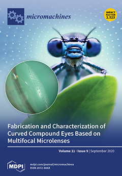
Bioinspired compound eyes have drawn extensive attention in recent years for their wide field of view, compact structure, and sensitive response to moving objects. However, the application of the element in optical systems is restricted by the manufacture of massive multifocal microlenses on a curvature-controllable spherical surface. In this paper, we propose a fabrication of a one-lens compound eye by combining photolithography, hot embossing, soft photolithography, and gas-assisted deformation techniques, and the ommatidia in different positions can steer and focus incident rays on the same plane. Our approach paves a way towards the convenient integration of compound eyes in medical imaging and military monitoring systems. View this paper
  • Issues are regarded as officially published after their release is announced to the table of contents alert mailing list.
  • You may sign up for e-mail alerts to receive table of contents of newly released issues.
  • PDF is the official format for papers published in both, html and pdf forms. To view the papers in pdf format, click on the "PDF Full-text" link, and use the free Adobe Reader to open them.
Order results
Result details
Section
Select all
Export citation of selected articles as:
13 pages, 1848 KiB  
Article
Single-Cell Elasticity Measurement with an Optically Actuated Microrobot
by István Grexa, Tamás Fekete, Judit Molnár, Kinga Molnár, Gaszton Vizsnyiczai, Pál Ormos and Lóránd Kelemen
Micromachines 2020, 11(9), 882; https://doi.org/10.3390/mi11090882 - 22 Sep 2020
Cited by 17 | Viewed by 3137
Abstract
A cell elasticity measurement method is introduced that uses polymer microtools actuated by holographic optical tweezers. The microtools were prepared with two-photon polymerization. Their shape enables the approach of the cells in any lateral direction. In the presented case, endothelial cells grown on [...] Read more.
A cell elasticity measurement method is introduced that uses polymer microtools actuated by holographic optical tweezers. The microtools were prepared with two-photon polymerization. Their shape enables the approach of the cells in any lateral direction. In the presented case, endothelial cells grown on vertical polymer walls were probed by the tools in a lateral direction. The use of specially shaped microtools prevents the target cells from photodamage that may arise during optical trapping. The position of the tools was recorded simply with video microscopy and analyzed with image processing methods. We critically compare the resulting Young’s modulus values to those in the literature obtained by other methods. The application of optical tweezers extends the force range available for cell indentations measurements down to the fN regime. Our approach demonstrates a feasible alternative to the usual vertical indentation experiments. Full article
(This article belongs to the Special Issue New Trends and Applications in Femtosecond Laser Micromachining)
Show Figures

Graphical abstract

15 pages, 4989 KiB  
Article
Accelerating the Finite-Element Method for Reaction-Diffusion Simulations on GPUs with CUDA
by Hedi Sellami, Leo Cazenille, Teruo Fujii, Masami Hagiya, Nathanael Aubert-Kato and Anthony J. Genot
Micromachines 2020, 11(9), 881; https://doi.org/10.3390/mi11090881 - 22 Sep 2020
Cited by 2 | Viewed by 2902
Abstract
DNA nanotechnology offers a fine control over biochemistry by programming chemical reactions in DNA templates. Coupled to microfluidics, it has enabled DNA-based reaction-diffusion microsystems with advanced spatio-temporal dynamics such as traveling waves. The Finite Element Method (FEM) is a standard tool to simulate [...] Read more.
DNA nanotechnology offers a fine control over biochemistry by programming chemical reactions in DNA templates. Coupled to microfluidics, it has enabled DNA-based reaction-diffusion microsystems with advanced spatio-temporal dynamics such as traveling waves. The Finite Element Method (FEM) is a standard tool to simulate the physics of such systems where boundary conditions play a crucial role. However, a fine discretization in time and space is required for complex geometries (like sharp corners) and highly nonlinear chemistry. Graphical Processing Units (GPUs) are increasingly used to speed up scientific computing, but their application to accelerate simulations of reaction-diffusion in DNA nanotechnology has been little investigated. Here we study reaction-diffusion equations (a DNA-based predator-prey system) in a tortuous geometry (a maze), which was shown experimentally to generate subtle geometric effects. We solve the partial differential equations on a GPU, demonstrating a speedup of ∼100 over the same resolution on a 20 cores CPU. Full article
(This article belongs to the Special Issue Recent Advances of Molecular Machines and Molecular Robots)
Show Figures

Figure 1

13 pages, 2955 KiB  
Article
Low-Cost Graphene-Based Digital Microfluidic System
by Mohamed Yafia, Amir M. Foudeh, Maryam Tabrizian and Homayoun Najjaran
Micromachines 2020, 11(9), 880; https://doi.org/10.3390/mi11090880 - 22 Sep 2020
Cited by 3 | Viewed by 2881
Abstract
In this work, the laser-scribing technique was used as a low-cost, rapid and facile method for fabricating digital microfluidic (DMF) systems. Laser-scribed graphene (LSG) electrodes are directly synthesized on flexible substrates to pattern the DMF electrode arrays. This facilitates the DMF electrodes’ fabrication [...] Read more.
In this work, the laser-scribing technique was used as a low-cost, rapid and facile method for fabricating digital microfluidic (DMF) systems. Laser-scribed graphene (LSG) electrodes are directly synthesized on flexible substrates to pattern the DMF electrode arrays. This facilitates the DMF electrodes’ fabrication process by eliminating many microfabrication steps. An electrowetting test was performed to investigate the effectiveness of the LSG DMF electrodes in changing the contact angles of droplets. Different DMF operations were successfully performed using the proposed LSG DMF chips in both open and closed DMF systems. The quality and output resolution were examined to assess the performance of such patterned electrodes in the DMF systems. To verify the efficacy of the LSG DMF chips, a one-step direct assay for the detection of Legionellapneumophila deoxyribonucleic acid (DNA) was performed on the chip without the need for any washing step. The high specificity in distinguishing a single-nucleotide mismatch was achieved by detecting target DNA concentrations as low as 1 nM. Our findings suggest that the proposed rapid and easy fabrication method for LSG DMF electrodes offers a great platform for low-cost and easily accessible point-of-care diagnostic devices. Full article
Show Figures

Figure 1

4 pages, 187 KiB  
Editorial
Editorial for the Special Issue “Selected Papers from the ISTEGIM’19—Thermal Effects in Gas Flow in Microscale”
by Lucien Baldas, Jürgen J. Brandner and Gian Luca Morini
Micromachines 2020, 11(9), 879; https://doi.org/10.3390/mi11090879 - 21 Sep 2020
Viewed by 1834
11 pages, 3299 KiB  
Article
Revealing the Plastic Mode of Time-Dependent Deformation of a LiTaO3 Single Crystal by Nanoindentation
by Shengyun Zhou, Xianwei Huang, Congda Lu, Yunfeng Liu, Taihua Zhang and Yi Ma
Micromachines 2020, 11(9), 878; https://doi.org/10.3390/mi11090878 - 21 Sep 2020
Cited by 2 | Viewed by 1963
Abstract
Recently, instrumental nanoindentation has been widely applied to detect time-dependent plastic deformation or creep behavior in numerous materials, particularly thin films and heterogeneous materials. However, deformation mechanism at nanoindentation holding stage has not been well revealed hitherto. In the current work, nanoindentation holding [...] Read more.
Recently, instrumental nanoindentation has been widely applied to detect time-dependent plastic deformation or creep behavior in numerous materials, particularly thin films and heterogeneous materials. However, deformation mechanism at nanoindentation holding stage has not been well revealed hitherto. In the current work, nanoindentation holding tests with high loads were performed on a brittle LiTaO3 single crystal. The surface morphologies of residual impressions with various holding times were investigated. It was indicated that generation of secondary cracks and propagation of both main and secondary cracks were the dominating mechanism for time-dependent plastic deformation at the initial holding stage, and the density and length of cracks were invariable at the steady-state holding stage, which suggested a nonlocalized plastic deformation beneath the indenter. It could be concluded that time-dependent plastic deformation of brittle ceramic under nanoindentation is composed of instant cracking as the continuation of loading sequence and homogeneous creep flow by high shear-compression stress at room temperature. Full article
Show Figures

Figure 1

10 pages, 6959 KiB  
Article
Cu(In,Ga)Se2 Solar Cells Integrated with Subwavelength Structured Cover Glass Fabricated by One-Step Self-Masked Etching
by Ho-Jung Jeong, Ye-Chan Kim, Sung-Tae Kim, Min-Ho Choi, Young-Hyun Song, Ju-Hyung Yun, Min-Su Park and Jae-Hyung Jang
Micromachines 2020, 11(9), 877; https://doi.org/10.3390/mi11090877 - 21 Sep 2020
Cited by 2 | Viewed by 2448
Abstract
We report an anti-reflective cover glass for Cu(In,Ga)Se2 (CIGS) thin film solar cells. Subwavelength structures (SWSs) were fabricated on top of a cover glass using one-step self-masked etching. The etching method resulted in dense whiskers with high aspect ratio. The produced structure [...] Read more.
We report an anti-reflective cover glass for Cu(In,Ga)Se2 (CIGS) thin film solar cells. Subwavelength structures (SWSs) were fabricated on top of a cover glass using one-step self-masked etching. The etching method resulted in dense whiskers with high aspect ratio. The produced structure exhibited excellent anti-reflective properties over a broad wavelength range, from the ultraviolet to the near infrared. Compared to a flat-surface glass, the average transmittance of the glass integrated with the SWSs improved from 92.4% to 95.2%. When the cover glass integrated with the SWSs was mounted onto the top of a CIGS device, the short-circuit current and the efficiency of the solar cell were enhanced by 4.38 and 6%, respectively, compared with a CIGS solar cell without cover glass. Full article
Show Figures

Graphical abstract

17 pages, 4921 KiB  
Article
Application of Miniature FBG-MEMS Pressure Sensor in Penetration Process of Jacked Pile
by Xueying Liu, Yonghong Wang and Mingyi Zhang
Micromachines 2020, 11(9), 876; https://doi.org/10.3390/mi11090876 - 21 Sep 2020
Cited by 7 | Viewed by 2387
Abstract
In order to study the penetration mechanism of jacked piles in viscous soil foundation, the stress variation law of the pile–soil interface was obtained by installing silicon piezoresistive earth pressure and pore water pressure sensors, and fiber Bragg grating (FBG) sensors in a [...] Read more.
In order to study the penetration mechanism of jacked piles in viscous soil foundation, the stress variation law of the pile–soil interface was obtained by installing silicon piezoresistive earth pressure and pore water pressure sensors, and fiber Bragg grating (FBG) sensors in a model pile body, and the penetration characteristics of jacked piles in homogeneous viscous soil were defined. The test results show that: Fiber Bragg grating and silicon piezoresistive sensing technology can better meet the requirements of testing the characteristics of jacked pile in viscous soil. The ratio of pile lateral resistance to pile end resistance varies when pile is jacked in homogeneous viscous soil. In the early stage of pile jacking, the ratio of pile lateral resistance is small, and in the later stage of pile jacking, the ratio of pile lateral resistance increases, but the ratio of pile end resistance is still higher than that of pile lateral resistance. The ratio of the effective stress to the total radial stress is high, and the variation law of the two is consistent with the depth. The total radial stress, pore water pressure, and effective radial stress all exhibit the degradation phenomenon, and the degradation degree decreases gradually with the increase in penetration depth at the same depth. The ratio of excess pore water pressure to overburden weight decreases with the increase in depth, and the maximum value is 87%. The research results can provide a reference for the engineering practice of jacked pile in viscous soil foundation. Full article
Show Figures

Figure 1

12 pages, 3849 KiB  
Article
Investigation of AlGaN/GaN HFET and VO2 Thin Film Based Deflection Transducers Embedded in GaN Microcantilevers
by Ferhat Bayram, Durga Gajula, Digangana Khan and Goutam Koley
Micromachines 2020, 11(9), 875; https://doi.org/10.3390/mi11090875 - 20 Sep 2020
Cited by 3 | Viewed by 2232
Abstract
The static and dynamic deflection transducing performances of piezotransistive AlGaN/GaN heterojunction field effect transistors (HFET) and piezoresistive VO2 thin films, fabricated on GaN microcantilevers of similar dimensions, were investigated. Deflection sensitivities were tuned with the gate bias and operating temperature for embedded [...] Read more.
The static and dynamic deflection transducing performances of piezotransistive AlGaN/GaN heterojunction field effect transistors (HFET) and piezoresistive VO2 thin films, fabricated on GaN microcantilevers of similar dimensions, were investigated. Deflection sensitivities were tuned with the gate bias and operating temperature for embedded AlGaN/GaN HFET and VO2 thin film transducers, respectively. The GaN microcantilevers were excited with a piezoactuator in their linear and nonlinear oscillation regions of the fundamental oscillatory mode. In the linear regime, the maximum deflection sensitivity of piezotransistive AlGaN/GaN HFET reached up to a 0.5% change in applied drain voltage, while the responsivity of the piezoresistive VO2 thin film based deflection transducer reached a maximum value of 0.36% change in applied drain current. The effects of the gate bias and the operation temperature on nonlinear behaviors of the microcantilevers were also experimentally examined. Static deflection sensitivity measurements demonstrated a large change of 16% in drain-source resistance of the AlGaN/GaN HFET, and a similarly high 11% change in drain-source resistance in the VO2 thin film, corresponding to a 10 μm downward step bending of the cantilever free end. Full article
(This article belongs to the Special Issue MEMS/NEMS Sensors: Fabrication and Application, Volume II)
Show Figures

Figure 1

3 pages, 148 KiB  
Editorial
Editorial for the Special Issue on the ICAE 2019
by Hongsoo Choi, Dong-Weon Lee, Jeong-Bong Lee and Sang-Jae Kim
Micromachines 2020, 11(9), 874; https://doi.org/10.3390/mi11090874 - 20 Sep 2020
Viewed by 1473
Abstract
This special issue is a collection of 10 selected papers after presenting at the Fifth International Conference on Advanced Electromaterials (ICAE 2019), held in Jeju, South Korea on 5–8 November 2019 [...] Full article
(This article belongs to the Special Issue Selected Papers from the ICAE 2019)
12 pages, 3021 KiB  
Article
Fused Deposition Modeling of Microfluidic Chips in Polymethylmethacrylate
by Frederik Kotz, Markus Mader, Nils Dellen, Patrick Risch, Andrea Kick, Dorothea Helmer and Bastian E. Rapp
Micromachines 2020, 11(9), 873; https://doi.org/10.3390/mi11090873 - 19 Sep 2020
Cited by 57 | Viewed by 6348
Abstract
Polymethylmethacrylate (PMMA) is one of the most important thermoplastic materials and is a widely used material in microfluidics. However, PMMA is usually structured using industrial scale replication processes, such as hot embossing or injection molding, not compatible with rapid prototyping. In this work, [...] Read more.
Polymethylmethacrylate (PMMA) is one of the most important thermoplastic materials and is a widely used material in microfluidics. However, PMMA is usually structured using industrial scale replication processes, such as hot embossing or injection molding, not compatible with rapid prototyping. In this work, we demonstrate that microfluidic chips made from PMMA can be 3D printed using fused deposition modeling (FDM). We demonstrate that using FDM microfluidic chips with a minimum channel cross-section of ~300 µm can be printed and a variety of different channel geometries and mixer structures are shown. The optical transparency of the chips is shown to be significantly enhanced by printing onto commercial PMMA substrates. The use of such commercial PMMA substrates also enables the integration of PMMA microstructures into the printed chips, by first generating a microstructure on the PMMA substrates, and subsequently printing the PMMA chip around the microstructure. We further demonstrate that protein patterns can be generated within previously printed microfluidic chips by employing a method of photobleaching. The FDM printing of microfluidic chips in PMMA allows the use of one of microfluidics’ most used industrial materials on the laboratory scale and thus significantly simplifies the transfer from results gained in the lab to an industrial product. Full article
(This article belongs to the Special Issue 3D Printing of MEMS Technology)
Show Figures

Figure 1

13 pages, 3020 KiB  
Article
The Microfluidic Trainer: Design, Fabrication and Validation of a Tool for Testing and Improving Manual Skills
by Francesco Costa, Luigi Falzetti, Nicola Baldini and Sofia Avnet
Micromachines 2020, 11(9), 872; https://doi.org/10.3390/mi11090872 - 19 Sep 2020
Viewed by 2359
Abstract
Microfluidic principles have been widely applied for more than 30 years to solve biological and micro-electromechanical problems. Despite the numerous advantages, microfluidic devices are difficult to manage as their handling comes with several technical challenges. We developed a new portable tool, the microfluidic [...] Read more.
Microfluidic principles have been widely applied for more than 30 years to solve biological and micro-electromechanical problems. Despite the numerous advantages, microfluidic devices are difficult to manage as their handling comes with several technical challenges. We developed a new portable tool, the microfluidic trainer (MT), that assesses the operator handling skills and that may be used for maintaining or improving the ability to inject fluid in the inlet of microfluidic devices for in vitro cell culture applications. After several tests, we optimized the MT tester cell to reproduce the real technical challenges of a microfluidic device. In addition to an exercise path, we included an overfilling indicator and a correct infilling indicator at the inlet (control path). We manufactured the MT by engraving a 3 mm-high sheet of methacrylate with 60W CO2 laser plotter to create multiple capillary paths. We validated the device by enrolling 21 volunteers (median age 33) to fill both the MT and a commercial microfluidic device. The success rate obtained with MT significantly correlated with those of a commercial microfluidic culture plate, and its 30 min-continuous use for three times significantly improved the performance. Overall, our data demonstrate that MT is a valid assessment tool of individual performances in using microfluidic devices and may represent a low-cost solution to training, improve or warm up microfluidic handling skills. Full article
Show Figures

Figure 1

25 pages, 7834 KiB  
Article
Full-Azimuth Beam Steering MIMO Antenna Arranged in a Daisy Chain Array Structure
by Kazuhiro Honda, Taiki Fukushima and Koichi Ogawa
Micromachines 2020, 11(9), 871; https://doi.org/10.3390/mi11090871 - 19 Sep 2020
Cited by 16 | Viewed by 5385
Abstract
This paper presents a multiple-input, multiple-output (MIMO) antenna system with the ability to perform full-azimuth beam steering, and with the aim of realizing greater than 20 Gbps vehicular communications. The MIMO antenna described in this paper comprises 64 elements arranged in a daisy [...] Read more.
This paper presents a multiple-input, multiple-output (MIMO) antenna system with the ability to perform full-azimuth beam steering, and with the aim of realizing greater than 20 Gbps vehicular communications. The MIMO antenna described in this paper comprises 64 elements arranged in a daisy chain array structure, where 32 subarrays are formed by pairing elements in each subarray; the antenna yields 32 independent subchannels for MIMO transmission, and covers all communication targets regardless of their position relative to the array. Analytical results reveal that the proposed antenna system can provide a channel capacity of more than 200 bits/s/Hz at a signal-to-noise power ratio (SNR) of 30 dB over the whole azimuth, which is equivalent to 20 Gbps for a bandwidth of 100 MHz. This remarkably high channel capacity is shown to be due to two significant factors; the improved directivity created by the optimum in-phase excitation and the low correlation between the subarrays due to the orthogonal alignment of the array with respect to the incident waves. Over-the-air (OTA) experiments confirm the increase in channel capacity; the proposed antenna can maintain a constant transmission rate over all azimuth angles. Full article
(This article belongs to the Special Issue Beam Steering via Arrayed Micromachines)
Show Figures

Figure 1

13 pages, 3254 KiB  
Article
A Direct Comparison between the Lateral Magnetophoretic Microseparator and AdnaTest for Isolating Prostate Circulating Tumor Cells
by Hyungseok Cho, Jae-Seung Chung and Ki-Ho Han
Micromachines 2020, 11(9), 870; https://doi.org/10.3390/mi11090870 - 19 Sep 2020
Cited by 8 | Viewed by 2770
Abstract
Circulating tumor cells (CTCs) are important biomarkers for the diagnosis, prognosis, and treatment of cancer. However, because of their extreme rarity, a more precise technique for isolating CTCs is required to gain deeper insight into the characteristics of cancer. This study compares the [...] Read more.
Circulating tumor cells (CTCs) are important biomarkers for the diagnosis, prognosis, and treatment of cancer. However, because of their extreme rarity, a more precise technique for isolating CTCs is required to gain deeper insight into the characteristics of cancer. This study compares the performance of a lateral magnetophoretic microseparator (“CTC-μChip”), as a representative microfluidic device, and AdnaTest ProstateCancer (Qiagen), as a commercially available specialized method, for isolating CTCs from the blood of patients with prostate cancer. The enumeration and genetic analysis results of CTCs isolated via the two methods were compared under identical conditions. In the CTC enumeration experiment, the number of CTCs isolated by the CTC-μChip averaged 17.67 CTCs/mL, compared to 1.56 CTCs/mL by the AdnaTest. The number of contaminating white blood cells (WBCs) and the CTC purity with the CTC-μChip averaged 772.22 WBCs/mL and 3.91%, respectively, whereas those with the AdnaTest averaged 67.34 WBCs/mL and 1.98%, respectively. Through genetic analysis, using a cancer-specific gene panel (AR (androgen receptor), AR-V7 (A\androgen receptor variant-7), PSMA (prostate specific membrane antigen), KRT19 (cytokeratin-19), CD45 (PTPRC, Protein tyrosine phosphatase, receptor type, C)) with reverse transcription droplet digital PCR, three genes (AR, AR-V7, and PSMA) were more highly expressed in cells isolated by the CTC-μChip, while KRT19 and CD45 were similarly detected using both methods. Consequently, this study showed that the CTC-μChip can be used to isolate CTCs more reliably than AdnaTest ProstateCancer, as a specialized method for gene analysis of prostate CTCs, as well as more sensitively obtain cancer-associated gene expressions. Full article
(This article belongs to the Special Issue Micro Process-Devices)
Show Figures

Figure 1

14 pages, 3548 KiB  
Article
Avalanche Transients of Thick 0.35 µm CMOS Single-Photon Avalanche Diodes
by Bernhard Goll, Bernhard Steindl and Horst Zimmermann
Micromachines 2020, 11(9), 869; https://doi.org/10.3390/mi11090869 - 19 Sep 2020
Cited by 4 | Viewed by 3059
Abstract
Two types of single-photon avalanche diodes (SPADs) with different diameters are investigated regarding their avalanche behavior. SPAD type A was designed in standard 0.35-µm complementary metal-oxide-semiconductor (CMOS) including a 12-µm thick p- epi-layer with diameters of 50, 100, 200, and 400 µm; [...] Read more.
Two types of single-photon avalanche diodes (SPADs) with different diameters are investigated regarding their avalanche behavior. SPAD type A was designed in standard 0.35-µm complementary metal-oxide-semiconductor (CMOS) including a 12-µm thick p- epi-layer with diameters of 50, 100, 200, and 400 µm; and type B was implemented in the high-voltage (HV) line of this process with diameters of 48.2 and 98.2 µm. Each SPAD is wire-bonded to a 0.35-µm CMOS clocked gating chip, which controls charge up to a maximum 6.6-V excess bias, active, and quench phase as well as readout during one clock period. Measurements of the cathode voltage after photon hits at SPAD type A resulted in fall times (80 to 20%) of 10.2 ns for the 50-µm diameter SPAD for an excess bias of 4.2 V and 3.45 ns for the 200-µm diameter device for an excess bias of 4.26 V. For type B, fall times of 8 ns for 48.2-µm diameter and 5.4-V excess bias as well as 2 ns for 98.2-µm diameter and 5.9-V excess bias were determined. In measuring the whole capacitance at the cathode of the SPAD with gating chip connected, the avalanche currents through the detector were calculated. This resulted in peak avalanche currents of, e.g., 1.19 mA for the 100-µm SPAD type A and 1.64 mA for the 98.2-µm SPAD type B for an excess bias of 5 and 4.9 V, respectively. Full article
Show Figures

Figure 1

13 pages, 4080 KiB  
Article
Surface Quality Improvement of 3D Microstructures Fabricated by Micro-EDM with a Composite 3D Microelectrode
by Jianguo Lei, Kai Jiang, Xiaoyu Wu, Hang Zhao and Bin Xu
Micromachines 2020, 11(9), 868; https://doi.org/10.3390/mi11090868 - 19 Sep 2020
Cited by 4 | Viewed by 2175
Abstract
Three-dimensional (3D) microelectrodes used for processing 3D microstructures in micro-electrical discharge machining (micro-EDM) can be readily prepared by laminated object manufacturing (LOM). However, the microelectrode surface always appears with steps due to the theoretical error of LOM, significantly reducing the surface quality of [...] Read more.
Three-dimensional (3D) microelectrodes used for processing 3D microstructures in micro-electrical discharge machining (micro-EDM) can be readily prepared by laminated object manufacturing (LOM). However, the microelectrode surface always appears with steps due to the theoretical error of LOM, significantly reducing the surface quality of 3D microstructures machined by micro-EDM with the microelectrode. To address the problem above, this paper proposes a filling method to fabricate a composite 3D microelectrode and applies it in micro-EDM for processing 3D microstructures without steps. The effect of bonding temperature and Sn film thickness on the steps is investigated in detail. Meanwhile, the distribution of Cu and Sn elements in the matrix and the steps is analyzed by the energy dispersive X-ray spectrometer. Experimental results show that when the Sn layer thickness on the interface is 8 μm, 15 h after heat preservation under 950 °C, the composite 3D microelectrodes without the steps on the surface were successfully fabricated, while Sn and Cu elements were evenly distributed in the microelectrodes. Finally, the composite 3D microelectrodes were applied in micro-EDM. Furthermore, 3D microstructures without steps on the surface were obtained. This study verifies the feasibility of machining 3D microstructures without steps by micro-EDM with a composite 3D microelectrode fabricated via the proposed method. Full article
Show Figures

Figure 1

13 pages, 3391 KiB  
Article
Seawater Desalination by Interfacial Solar Vapor Generation Method Using Plasmonic Heating Nanocomposites
by Zhourui Xu, Nanxi Rao, Chak-Yin Tang and Wing-Cheung Law
Micromachines 2020, 11(9), 867; https://doi.org/10.3390/mi11090867 - 18 Sep 2020
Cited by 6 | Viewed by 2816
Abstract
With the ever-growing demand in fresh water supply, great efforts have been devoted to developing sustainable systems which could generate fresh water continuously. Solar vapor generation is one of the promising strategies which comprise an unlimited energy source and efficient solar-to-heat generators for [...] Read more.
With the ever-growing demand in fresh water supply, great efforts have been devoted to developing sustainable systems which could generate fresh water continuously. Solar vapor generation is one of the promising strategies which comprise an unlimited energy source and efficient solar-to-heat generators for overcoming fresh water scarcity. However, current solar vapor generation systems suffer either from inefficient utilization of solar energy or an expensive fabrication process. In this paper, we introduced a nano-plasmonic approach, i.e., a floatable nanocompoiste where copper sulfide nanorods (Cu2-xS NRs) are embedded in a polyvinyl alcohol (PVA) matrix, for solar-to-vapor generation. A high solar vapor generation efficiency of ~87% and water evaporation rate of 1.270 kg m−2 h−1 were achieved under simulated solar irradiation of 1 sun. With the illumination of natural daylight, seawater was purified using Cu2-xS NRs-PVA gel, with high purity, as distilled drinking water. The plasmonic nanocomposites demonstrated here are easy to fabricate and highly efficient for solar vapor generation, illustrating a potential solution for future seawater desalination. Full article
(This article belongs to the Section D:Materials and Processing)
Show Figures

Figure 1

37 pages, 4817 KiB  
Review
Graphene Quantum Dots as Flourishing Nanomaterials for Bio-Imaging, Therapy Development, and Micro-Supercapacitors
by Merve Kortel, Bhargav D. Mansuriya, Nicole Vargas Santana and Zeynep Altintas
Micromachines 2020, 11(9), 866; https://doi.org/10.3390/mi11090866 - 18 Sep 2020
Cited by 50 | Viewed by 6823
Abstract
Graphene quantum dots (GQDs) are considerably a new member of the carbon family and shine amongst other members, thanks to their superior electrochemical, optical, and structural properties as well as biocompatibility features that enable us to engage them in various bioengineering purposes. Especially, [...] Read more.
Graphene quantum dots (GQDs) are considerably a new member of the carbon family and shine amongst other members, thanks to their superior electrochemical, optical, and structural properties as well as biocompatibility features that enable us to engage them in various bioengineering purposes. Especially, the quantum confinement and edge effects are giving GQDs their tremendous character, while their heteroatom doping attributes enable us to specifically and meritoriously tune their prospective characteristics for innumerable operations. Considering the substantial role offered by GQDs in the area of biomedicine and nanoscience, through this review paper, we primarily focus on their applications in bio-imaging, micro-supercapacitors, as well as in therapy development. The size-dependent aspects, functionalization, and particular utilization of the GQDs are discussed in detail with respect to their distinct nano-bio-technological applications. Full article
(This article belongs to the Special Issue Biosensors and MEMS-based Diagnostic Applications)
Show Figures

Graphical abstract

21 pages, 5529 KiB  
Review
A Review and Perspective for the Development of Triboelectric Nanogenerator (TENG)-Based Self-Powered Neuroprosthetics
by Hao Wang, Tianzhun Wu, Qi Zeng and Chengkuo Lee
Micromachines 2020, 11(9), 865; https://doi.org/10.3390/mi11090865 - 18 Sep 2020
Cited by 27 | Viewed by 5868
Abstract
Neuroprosthetics have become a powerful toolkit for clinical interventions of various diseases that affect the central nervous or peripheral nervous systems, such as deep brain stimulation (DBS), functional electrical stimulation (FES), and vagus nerve stimulation (VNS), by electrically stimulating different neuronal structures. To [...] Read more.
Neuroprosthetics have become a powerful toolkit for clinical interventions of various diseases that affect the central nervous or peripheral nervous systems, such as deep brain stimulation (DBS), functional electrical stimulation (FES), and vagus nerve stimulation (VNS), by electrically stimulating different neuronal structures. To prolong the lifetime of implanted devices, researchers have developed power sources with different approaches. Among them, the triboelectric nanogenerator (TENG) is the only one to achieve direct nerve stimulations, showing great potential in the realization of a self-powered neuroprosthetic system in the future. In this review, the current development and progress of the TENG-based stimulation of various kinds of nervous systems are systematically summarized. Then, based on the requirements of the neuroprosthetic system in a real application and the development of current techniques, a perspective of a more sophisticated neuroprosthetic system is proposed, which includes components of a thin-film TENG device with a biocompatible package, an amplification circuit to enhance the output, and a self-powered high-frequency switch to generate high-frequency current pulses for nerve stimulations. Then, we review and evaluate the recent development and progress of each part. Full article
(This article belongs to the Special Issue Implantable Microdevices, Volume II)
Show Figures

Figure 1

13 pages, 3666 KiB  
Article
Towards the Fabrication of High-Aspect-Ratio Silicon Gratings by Deep Reactive Ion Etching
by Zhitian Shi, Konstantins Jefimovs, Lucia Romano and Marco Stampanoni
Micromachines 2020, 11(9), 864; https://doi.org/10.3390/mi11090864 - 18 Sep 2020
Cited by 38 | Viewed by 7438
Abstract
The key optical components of X-ray grating interferometry are gratings, whose profile requirements play the most critical role in acquiring high quality images. The difficulty of etching grating lines with high aspect ratios when the pitch is in the range of a few [...] Read more.
The key optical components of X-ray grating interferometry are gratings, whose profile requirements play the most critical role in acquiring high quality images. The difficulty of etching grating lines with high aspect ratios when the pitch is in the range of a few micrometers has greatly limited imaging applications based on X-ray grating interferometry. A high etching rate with low aspect ratio dependence is crucial for higher X-ray energy applications and good profile control by deep reactive ion etching of grating patterns. To achieve this goal, a modified Coburn–Winters model was applied in order to study the influence of key etching parameters, such as chamber pressure and etching power. The recipe for deep reactive ion etching was carefully fine-tuned based on the experimental results. Silicon gratings with an area of 70 × 70 mm2, pitch size of 1.2 and 2 μm were fabricated using the optimized process with aspect ratio α of ~67 and 77, respectively. Full article
Show Figures

Figure 1

12 pages, 4324 KiB  
Article
Inkjet-Printed Graphene-Based 1 × 2 Phased Array Antenna
by Mahmuda Akter Monne, Peter Mack Grubb, Harold Stern, Harish Subbaraman, Ray T. Chen and Maggie Yihong Chen
Micromachines 2020, 11(9), 863; https://doi.org/10.3390/mi11090863 - 18 Sep 2020
Cited by 19 | Viewed by 3308
Abstract
Low-cost and conformal phased array antennas (PAAs) on flexible substrates are of particular interest in many applications. The major deterrents to developing flexible PAA systems are the difficulty in integrating antenna and electronics circuits on the flexible surface, as well as the bendability [...] Read more.
Low-cost and conformal phased array antennas (PAAs) on flexible substrates are of particular interest in many applications. The major deterrents to developing flexible PAA systems are the difficulty in integrating antenna and electronics circuits on the flexible surface, as well as the bendability and oxidation rate of radiating elements and electronics circuits. In this research, graphene ink was developed from graphene flakes and used to inkjet print the radiating element and the active channel of field effect transistors (FETs). Bending and oxidation tests were carried out to validate the application of printed flexible graphene thin films in flexible electronics. An inkjet-printed graphene-based 1 × 2 element phased array antenna was designed and fabricated. Graphene-based field effect transistors were used as switches in the true-time delay line of the phased array antenna. The graphene phased array antenna was 100% inkjet printed on top of a 5 mil flexible Kapton® substrate, at room temperature. Four possible azimuth steering angles were designed for −26.7°, 0°, 13°, and 42.4°. Measured far-field patterns show good agreement with simulation results. Full article
(This article belongs to the Special Issue Graphene based Electronic Devices)
Show Figures

Figure 1

26 pages, 8241 KiB  
Article
Microfabrication Process-Driven Design, FEM Analysis and System Modeling of 3-DoF Drive Mode and 2-DoF Sense Mode Thermally Stable Non-Resonant MEMS Gyroscope
by Syed Ali Raza Bukhari, Muhammad Mubasher Saleem, Umar Shahbaz Khan, Amir Hamza, Javaid Iqbal and Rana Iqtidar Shakoor
Micromachines 2020, 11(9), 862; https://doi.org/10.3390/mi11090862 - 17 Sep 2020
Cited by 14 | Viewed by 3836
Abstract
This paper presents microfabrication process-driven design of a multi-degree of freedom (multi-DoF) non-resonant electrostatic microelectromechanical systems (MEMS) gyroscope by considering the design constraints of commercially available low-cost and widely-used silicon-on-insulator multi-user MEMS processes (SOIMUMPs), with silicon as a structural material. The proposed design [...] Read more.
This paper presents microfabrication process-driven design of a multi-degree of freedom (multi-DoF) non-resonant electrostatic microelectromechanical systems (MEMS) gyroscope by considering the design constraints of commercially available low-cost and widely-used silicon-on-insulator multi-user MEMS processes (SOIMUMPs), with silicon as a structural material. The proposed design consists of a 3-DoF drive mode oscillator with the concept of addition of a collider mass which transmits energy from the drive mass to the passive sense mass. In the sense direction, 2-DoF sense mode oscillator is used to achieve dynamically-amplified displacement in the sense mass. A detailed analytical model for the dynamic response of MEMS gyroscope is presented and performance characteristics are validated through finite element method (FEM)-based simulations. The effect of operating air pressure and temperature variations on the air damping and resulting dynamic response is analyzed. The thermal stability of the design and corresponding effect on the mechanical and capacitive sensitivity, for an operating temperature range of −40 °C to 100 °C, is presented. The results showed that the proposed design is thermally stable, robust to environmental variations, and process tolerances with a wide operational bandwidth and high sensitivity. Moreover, a system-level model of the proposed gyroscope and its integration with the sensor electronics is presented to estimate the voltage sensitivity under the constraints of the readout electronic circuit. Full article
(This article belongs to the Special Issue Recent Advances in MEMS Gyroscope)
Show Figures

Figure 1

18 pages, 3232 KiB  
Article
A Tumbling Magnetic Microrobot System for Biomedical Applications
by Elizabeth E. Niedert, Chenghao Bi, Georges Adam, Elly Lambert, Luis Solorio, Craig J. Goergen and David J. Cappelleri
Micromachines 2020, 11(9), 861; https://doi.org/10.3390/mi11090861 - 17 Sep 2020
Cited by 24 | Viewed by 14895
Abstract
A microrobot system comprising an untethered tumbling magnetic microrobot, a two-degree-of-freedom rotating permanent magnet, and an ultrasound imaging system has been developed for in vitro and in vivo biomedical applications. The microrobot tumbles end-over-end in a net forward motion due to applied magnetic [...] Read more.
A microrobot system comprising an untethered tumbling magnetic microrobot, a two-degree-of-freedom rotating permanent magnet, and an ultrasound imaging system has been developed for in vitro and in vivo biomedical applications. The microrobot tumbles end-over-end in a net forward motion due to applied magnetic torque from the rotating magnet. By turning the rotational axis of the magnet, two-dimensional directional control is possible and the microrobot was steered along various trajectories, including a circular path and P-shaped path. The microrobot is capable of moving over the unstructured terrain within a murine colon in in vitro, in situ, and in vivo conditions, as well as a porcine colon in ex vivo conditions. High-frequency ultrasound imaging allows for real-time determination of the microrobot’s position while it is optically occluded by animal tissue. When coated with a fluorescein payload, the microrobot was shown to release the majority of the payload over a 1-h time period in phosphate-buffered saline. Cytotoxicity tests demonstrated that the microrobot’s constituent materials, SU-8 and polydimethylsiloxane (PDMS), did not show a statistically significant difference in toxicity to murine fibroblasts from the negative control, even when the materials were doped with magnetic neodymium microparticles. The microrobot system’s capabilities make it promising for targeted drug delivery and other in vivo biomedical applications. Full article
(This article belongs to the Special Issue Magnetic Microrobots)
Show Figures

Figure 1

22 pages, 10078 KiB  
Article
Electromechanical Modeling of Vibration-Based Piezoelectric Nanogenerator with Multilayered Cross-Section for Low-Power Consumption Devices
by Ernesto A. Elvira-Hernández, Juan C. Anaya-Zavaleta, Eustaquio Martínez-Cisneros, Francisco López-Huerta, Luz Antonio Aguilera-Cortés and Agustín L. Herrera-May
Micromachines 2020, 11(9), 860; https://doi.org/10.3390/mi11090860 - 17 Sep 2020
Cited by 2 | Viewed by 2546
Abstract
Piezoelectric nanogenerators can convert energy from ambient vibrations into electrical energy. In the future, these nanogenerators could substitute conventional electrochemical batteries to supply electrical energy to consumer electronics. The optimal design of nanogenerators is fundamental in order to achieve their best electromechanical behavior. [...] Read more.
Piezoelectric nanogenerators can convert energy from ambient vibrations into electrical energy. In the future, these nanogenerators could substitute conventional electrochemical batteries to supply electrical energy to consumer electronics. The optimal design of nanogenerators is fundamental in order to achieve their best electromechanical behavior. We present the analytical electromechanical modeling of a vibration-based piezoelectric nanogenerator composed of a double-clamped beam with five multilayered cross-sections. This nanogenerator design has a central seismic mass (910 μm thickness) and substrate (125 μm thickness) of polyethylene terephthalate (PET) as well as a zinc oxide film (100 nm thickness) at the bottom of each end. The zinc oxide (ZnO) films have two aluminum electrodes (100 nm thickness) through which the generated electrical energy is extracted. The analytical electromechanical modeling is based on the Rayleigh method, Euler–Bernoulli beam theory and Macaulay method. In addition, finite element method (FEM) models are developed to estimate the electromechanical behavior of the nanogenerator. These FEM models consider air damping at atmospheric pressure and optimum load resistance. The analytical modeling results agree well with respect to those of FEM models. For applications under accelerations in y-direction of 2.50 m/s2 and an optimal load resistance of 32,458 Ω, the maximum output power and output power density of the nanogenerator at resonance (119.9 Hz) are 50.44 μW and 82.36 W/m3, respectively. This nanogenerator could be used to convert the ambient mechanical vibrations into electrical energy and supply low-power consumption devices. Full article
Show Figures

Graphical abstract

12 pages, 2635 KiB  
Communication
Broadband High-Efficiency Grating Couplers for Perfectly Vertical Fiber-to-Chip Coupling Enhanced by Fabry-Perot-like Cavity
by Zan Zhang, Beiju Huang, Zanyun Zhang, Chuantong Cheng, Bing Bai, Tianxi Gao, Xiaobo Xu, Wenping Gu, Lin Zhang and Hongda Chen
Micromachines 2020, 11(9), 859; https://doi.org/10.3390/mi11090859 - 17 Sep 2020
Cited by 1 | Viewed by 2820
Abstract
We propose a broadband high-efficiency grating coupler for perfectly vertical fiber-to-chip coupling. The up-reflection is reduced, hence enhanced coupling efficiency is achieved with the help of a Fabry-Perot-like cavity composed of a silicon nitride reflector and the grating itself. With the theory of [...] Read more.
We propose a broadband high-efficiency grating coupler for perfectly vertical fiber-to-chip coupling. The up-reflection is reduced, hence enhanced coupling efficiency is achieved with the help of a Fabry-Perot-like cavity composed of a silicon nitride reflector and the grating itself. With the theory of the Fabry-Perot cavity, the dimensional parameters of the coupler are investigated. With the optimized parameters, up-reflection in the C-band is reduced from 10.6% to 5%, resulting in an enhanced coupling efficiency of 80.3%, with a 1-dB bandwidth of 58 nm, which covers the entire C-band. The minimum feature size of the proposed structure is over 219 nm, which makes our design easy to fabricate through 248 nm deep-UV lithography, and lowers the fabrication cost. The proposed design has potential in efficient and fabrication-tolerant interfacing applications, between off-chip light sources and integrated chips that can be mass-produced. Full article
(This article belongs to the Special Issue Silicon Photonics Bloom, Volume II)
Show Figures

Figure 1

14 pages, 3318 KiB  
Article
Electrochemical Performance of Micropillar Array Electrodes in Microflows
by Bo Liu, Chuanwen Lv, Chaozhan Chen, Bin Ran, Minbo Lan, Huaying Chen and Yonggang Zhu
Micromachines 2020, 11(9), 858; https://doi.org/10.3390/mi11090858 - 17 Sep 2020
Cited by 11 | Viewed by 3174
Abstract
The microchip-based electrochemical detection system (μEDS) has attracted plenty of research attention due to its merits including the capability in high-density integration, high sensitivity, fast analysis time, and reduced reagent consumption. The miniaturized working electrode is usually regarded as the core component of [...] Read more.
The microchip-based electrochemical detection system (μEDS) has attracted plenty of research attention due to its merits including the capability in high-density integration, high sensitivity, fast analysis time, and reduced reagent consumption. The miniaturized working electrode is usually regarded as the core component of the μEDS, since its characteristic directly determines the performance of the whole system. Compared with the microelectrodes with conventional shapes such as the band, ring and disk, the three-dimensional (3D) micropillar array electrode (μAE) has demonstrated significant potential in improving the current response and decreasing the limits of detection due to its much larger reaction area. In this study, the numerical simulation method was used to investigate the performance of the μEDS, and both the geometrical and hydrodynamic parameters, including the micropillars shape, height, arrangement form and the flow rate of the reactant solution, were taken into consideration. The tail effect in μAEs was also quantitatively analyzed based on a pre-defined parameter of the current density ratio. In addition, a PDMS-based 3D μAE was fabricated and integrated into the microchannel for the electrochemical detection. The experiments of cyclic voltammetry (CV) and chronoamperometry (CA) were conducted, and a good agreement was found between the experimental and simulation results. This study would be instructive for the configuration and parameters design of the μEDS, and the presented method can be adopted to analyze and optimize the performance of nanochip-based electrochemical detection system (nEDS). Full article
(This article belongs to the Special Issue Advances in Nanofluidics)
Show Figures

Figure 1

11 pages, 2684 KiB  
Article
Bending Properties of Carbon Nanotube/Polymer Composites with Various Aspect Ratios and Filler Contents
by Oh-Nyoung Hur, Hyun-Woo Kim and Sung-Hoon Park
Micromachines 2020, 11(9), 857; https://doi.org/10.3390/mi11090857 - 17 Sep 2020
Cited by 6 | Viewed by 2340
Abstract
The key characteristics of bending sensors are piezoresistive effect, hysteresis, and durability. In this study, to investigate the influence of the aspect ratio and contents of multi-walled nanotubes (MWNTs) on the properties of bending sensors, MWNT/polydimethylsiloxane (PDMS) composites were fabricated with various aspect [...] Read more.
The key characteristics of bending sensors are piezoresistive effect, hysteresis, and durability. In this study, to investigate the influence of the aspect ratio and contents of multi-walled nanotubes (MWNTs) on the properties of bending sensors, MWNT/polydimethylsiloxane (PDMS) composites were fabricated with various aspect ratios and filler contents. The MWNTs were uniformly dispersed in the composites using the three-roll milling method. By increasing the bending angle gradually, the sensitivity of each composite was analyzed. Furthermore, discontinuous cyclic bending tests were conducted to investigate the piezoresistive effect and hysteresis. In addition, stable repeatability of the composites was confirmed through continuous cyclic bending tests. As a result, optimal aspect ratios and filler contents have been presented for application in bending sensors of MWNT composites. Full article
(This article belongs to the Special Issue Organic Electronic Devices, Volume II)
Show Figures

Figure 1

12 pages, 8357 KiB  
Communication
Single-Cell Electroporation with Real-Time Impedance Assessment Using a Constriction Microchannel
by Yifei Ye, Xiaofeng Luan, Lingqian Zhang, Wenjie Zhao, Jie Cheng, Mingxiao Li, Yang Zhao and Chengjun Huang
Micromachines 2020, 11(9), 856; https://doi.org/10.3390/mi11090856 - 16 Sep 2020
Cited by 8 | Viewed by 3747
Abstract
The electroporation system can serve as a tool for the intracellular delivery of foreign cargos. However, this technique is presently limited by the inaccurate electric field applied to the single cells and lack of a real-time electroporation metrics subsystem. Here, we reported a [...] Read more.
The electroporation system can serve as a tool for the intracellular delivery of foreign cargos. However, this technique is presently limited by the inaccurate electric field applied to the single cells and lack of a real-time electroporation metrics subsystem. Here, we reported a microfluidic system for precise and rapid single-cell electroporation and simultaneous impedance monitoring in a constriction microchannel. When single cells (A549) were continuously passing through the constriction microchannel, a localized high electric field was applied on the cell membrane, which resulted in highly efficient (up to 96.6%) electroporation. During a single cell entering the constriction channel, an abrupt impedance drop was noticed and demonstrated to be correlated with the occurrence of electroporation. Besides, while the cell was moving in the constriction channel, the stabilized impedance showed the capability to quantify the electroporation extent. The correspondence of the impedance variation and electroporation was validated by the intracellular delivery of the fluorescence indicator (propidium iodide). Based on the obtained results, this system is capable of precise control of electroporation and real-time, label-free impedance assessment, providing a potential tool for intracellular delivery and other biomedical applications. Full article
(This article belongs to the Special Issue Microfluidics for Cells and Other Organisms, Volume II)
Show Figures

Figure 1

24 pages, 3665 KiB  
Review
Microphysiological Systems for Neurodegenerative Diseases in Central Nervous System
by Mihyeon Bae, Hee-Gyeong Yi, Jinah Jang and Dong-Woo Cho
Micromachines 2020, 11(9), 855; https://doi.org/10.3390/mi11090855 - 16 Sep 2020
Cited by 10 | Viewed by 5014
Abstract
Neurodegenerative diseases are among the most severe problems in aging societies. Various conventional experimental models, including 2D and animal models, have been used to investigate the pathogenesis of (and therapeutic mechanisms for) neurodegenerative diseases. However, the physiological gap between humans and the current [...] Read more.
Neurodegenerative diseases are among the most severe problems in aging societies. Various conventional experimental models, including 2D and animal models, have been used to investigate the pathogenesis of (and therapeutic mechanisms for) neurodegenerative diseases. However, the physiological gap between humans and the current models remains a hurdle to determining the complexity of an irreversible dysfunction in a neurodegenerative disease. Therefore, preclinical research requires advanced experimental models, i.e., those more physiologically relevant to the native nervous system, to bridge the gap between preclinical stages and patients. The neural microphysiological system (neural MPS) has emerged as an approach to summarizing the anatomical, biochemical, and pathological physiology of the nervous system for investigation of neurodegenerative diseases. This review introduces the components (such as cells and materials) and fabrication methods for designing a neural MPS. Moreover, the review discusses future perspectives for improving the physiological relevance to native neural systems. Full article
Show Figures

Graphical abstract

12 pages, 3882 KiB  
Article
Fabrication and Characterization of Curved Compound Eyes Based on Multifocal Microlenses
by Gaoge Lian, Yongshun Liu, KeKai Tao, Huaming Xing, Ruxia Huang, Mingbo Chi, Wenchao Zhou and Yihui Wu
Micromachines 2020, 11(9), 854; https://doi.org/10.3390/mi11090854 - 16 Sep 2020
Cited by 17 | Viewed by 3206
Abstract
Curved compound eyes have generated great interest owing to the wide field of view but the application of devices is hindered for the lack of proper detectors. One-lens curved compound eyes with multi-focal microlenses provide a solution for wide field imaging integrated in [...] Read more.
Curved compound eyes have generated great interest owing to the wide field of view but the application of devices is hindered for the lack of proper detectors. One-lens curved compound eyes with multi-focal microlenses provide a solution for wide field imaging integrated in a commercial photo-detector. However, it is still a challenge for manufacturing this kind of compound eye. In this paper, a rapid and accurate method is proposed by a combination of photolithography, hot embossing, soft photolithography, and gas-assisted deformation techniques. Microlens arrays with different focal lengths were firstly obtained on a polymer, and then the planar structure was converted to the curved surface. A total of 581 compound eyes with diameters ranging from 152.8 µm to 240.9 µm were successfully obtained on one curved surface within a few hours, and the field of view of the compound eyes exceeded 108°. To verify the characteristics of the fabricated compound eyes, morphology deviation was measured by a probe profile and a scanning electron microscope. The optical performance and imaging capability were also tested and analyzed. As a result, the ommatidia made up of microlenses showed not only high accuracy in morphology, but also imaging uniformity on a focal plane. This flexible massive fabrication of compound eyes indicates great potential for miniaturized imaging systems. Full article
Show Figures

Figure 1

17 pages, 15468 KiB  
Review
Miniaturization and 3D Printing of Bioreactors: A Technological Mini Review
by Spyridon Achinas, Jorn-Ids Heins, Janneke Krooneman and Gerrit Jan Willem Euverink
Micromachines 2020, 11(9), 853; https://doi.org/10.3390/mi11090853 - 14 Sep 2020
Cited by 6 | Viewed by 5031
Abstract
Many articles have been published on scale-down concepts as well as additive manufacturing techniques. However, information is scarce when miniaturization and 3D printing are applied in the fabrication of bioreactor systems. Therefore, garnering information for the interfaces between miniaturization and 3D printing becomes [...] Read more.
Many articles have been published on scale-down concepts as well as additive manufacturing techniques. However, information is scarce when miniaturization and 3D printing are applied in the fabrication of bioreactor systems. Therefore, garnering information for the interfaces between miniaturization and 3D printing becomes important and essential. The first goal is to examine the miniaturization aspects concerning bioreactor screening systems. The second goal is to review successful modalities of 3D printing and its applications in bioreactor manufacturing. This paper intends to provide information on anaerobic digestion process intensification by fusion of miniaturization technique and 3D printing technology. In particular, it gives a perspective on the challenges of 3D printing and the options of miniature bioreactor systems for process high-throughput screening. Full article
(This article belongs to the Special Issue Biofabrication and 3D Bioprinting)
Show Figures

Figure 1

Previous Issue
Next Issue
Back to TopTop