1. Introduction
Low-temperature wafer bonding is increasingly required due to the increasing use of heterogeneous integrations [
1,
2,
3]. An effective approach to such bonding is to use intermediate layers [
4,
5]. Gold (Au) is a good candidate material for these bonding layers because of its high electrical and thermal conductivity, good deformability, and high oxidation resistance.
Several Au–Au bonding techniques have been investigated to achieve low-temperature bonding, including thermocompression bonding [
6,
7,
8,
9,
10,
11,
12], atomic diffusion bonding [
4,
13,
14], and surface activated bonding (SAB) [
15,
16,
17,
18,
19]. With SAB, the surfaces to be bonded are activated by plasma pretreatment and then bonded at low temperature (<150 °C). Furthermore, the use of Au for the bonding layer enables bonding in ambient air because gold oxide (Au
2O
3) is the only metal oxide that has a positive formation enthalpy (+19.3 kJ/mol) [
20]. The use of SAB with little contact pressure at room temperature in ambient air using ultrathin (<50 nm) Au films with smooth (root mean square (RMS) <0.50 nm) surfaces was recently shown to result in reliable Au–Au bonding [
17].
While Ar plasma is commonly used to activate Au surfaces by physically bombarding them with Ar ions or atoms, O
2 plasma is commonly used to clean surfaces because it can eliminate organic contaminants by chemical reaction [
21,
22]. It is also used for pretreatment before Au–Au bonding; O
2 plasma treatment has been reported to more effectively improve Au wire bond interfacial adhesion than Ar plasma treatment [
23,
24]. However, the Au–Au bonding may be weakened by the mixing of O
2 gas into the plasma processing gas [
25,
26]. The effect of plasma treatment, and especially the effect of O
2 plasma treatment on Au–Au bonding, thus needs further investigation.
This paper reports the investigation of Ar plasma vs. O2 plasma as a pretreatment method for room-temperature wafer-scale Au–Au bonding using ultrathin Au films (<50 nm) in ambient air. The main difference between Ar plasma and O2 plasma is their surface activation mechanism: physical etching and chemical reaction, respectively. The investigation included an analysis of Au surfaces treated with Ar or O2 plasma.
2. Materials and Methods
Silicon substrates with Au film and a Ti adhesion layer were used for analysis and bonding. A Ti adhesion layer followed by Au thin film was deposited on a Si substrate or a thermally oxidized Si substrate by direct current (DC) sputtering at a substrate temperature of 25 °C. The Ar or O2 plasma used to activate the surfaces was generated by applying 200 W radio frequency (RF) power at 60 Pa. Both plasmas were generated using the same equipment; only the process gas was changed.
The effect of each plasma treatment on the surface properties was determined by evaluating the surface roughness, hydrophilicity, electrical characteristics, and chemical state of the Au surfaces before and after each treatment. Surface roughness was measured using an atomic force microscope (AFM, Hitachi High-Tech Science Co., Tokyo, Japan, L-trace) and Si wafers with Au thin film (thickness: 15 nm) and a Ti adhesion layer (thickness: 5 nm). The AFM measurement was performed with a scan area of 500 nm × 500 nm and a resolution of 256 × 256 pixels. Hydrophilicity was evaluated by measuring the contact angle of the Au surfaces as measured with a contact angle meter (Kyowa Interface Science Co, Ltd., Saitama, Japan, PCA-11). Pure water (1.5 µL) was dropped on the Au surfaces, and the contact angle was calculated using the half-angle method. The electrical characteristics were evaluated by four-point measurement of the sheet resistance using a resistivity processor (NPS Inc., Tokyo, Japan, Model Σ) and Si wafers with Au thin film (thickness: 15 nm) and a Ti adhesion layer (thickness: 5 nm). The effect of the plasma treatment time was measured by irradiating plasma onto the same wafer several times. The surface chemical states were determined using X-ray photoelectron spectroscopy (XPS) analysis and thermal desorption spectrometry (TDS) analysis. The XPS analysis was performed using an X-ray photoelectron spectroscope (JEOL Ltd., Tokyo, Japan, JPS9200-T). A non-monochromatic Mg Kα source (photon energy: 1253.6 eV) was used at an operating power of 10 kV × 10 mA. Smoothing, Shirley-type background subtraction, and charge correction using the Au 4f7/2 binding energy were performed. The TDS analysis was performed using a thermal desorption spectrometer (ESCO Ltd., Tokyo, Japan, EMD-WA1000S). Thicker Au films (thickness: 300 nm) with Ti adhesion layers (thickness: 5 nm) deposited on thermally oxidized Si substrates were used to avoid the effect of diffusion from the adhesion layer or Si substrate during annealing. The temperature was increased at a rate of 30 °C/min and was corrected by measurement using a dummy Si substrate.
Four-inch Si wafers with Au thin film (thickness: 15 nm) and a Ti adhesion layer (thickness: 5 nm) were bonded after Ar or O2 plasma treatment in ambient air by overlapping two wafers and pinching the wafers together with tweezers. Bond front propagation was observed using an infrared (IR) transmission setup. The effects of plasma treatment time and air exposure time after plasma treatment on self-propagation of the bonding area and on bonding strength were investigated. The effects of annealing before bonding on the self-propagation of the bonding area and on bonding strength were also investigated by annealing wafers that had been plasma-treated up to 150 °C for 10 min in vacuum and then bonding them together in ambient air at room temperature.
Bonding strength was measured using destructive razor blade testing, also known as the crack opening or double cantilever beam method [
27,
28]. This testing method is an effective way to evaluate the energy of the bonded surfaces (i.e., surface energy). It is performed by inserting a razor blade between the bonded wafer pairs and observing the crack length along the bonded interface. The surface energy
γ (J/m
2) (i.e., half the bonding energy
G) was calculated under plane strain conditions and the assumptions of beam theory using
where
E (Pa) is the Young’s modulus of the wafer,
Tb (m) is the blade thickness,
Tw (m) is the wafer thickness, and
L (m) is the crack length [
27]. In this experiment, Si substrates with a thickness of
525 μm and a blade with a thickness of 100 µm were used. For calculation, we assumed that Si is isotropic, with Young’s modulus of elasticity
E = 169 GPa [
29,
30]. Although the measurement should be conducted using beam-shaped samples in order to accurately determine the surface energy [
31], we used whole bonded wafer pairs because the fabrication of beam-shaped samples is particularly difficult for weakly bonded wafer pairs. The crack length along the bonded interface was observed with an IR camera in a standard clean room atmosphere. Since values obtained from Equation (1) are affected by the crack detection resolution, anisotropic mechanical properties, and humidity environment [
28,
30], the comparison of absolute energy values with published results requires careful consideration.
3. Results
3.1. Surface Analysis
3.1.1. AFM Measurement
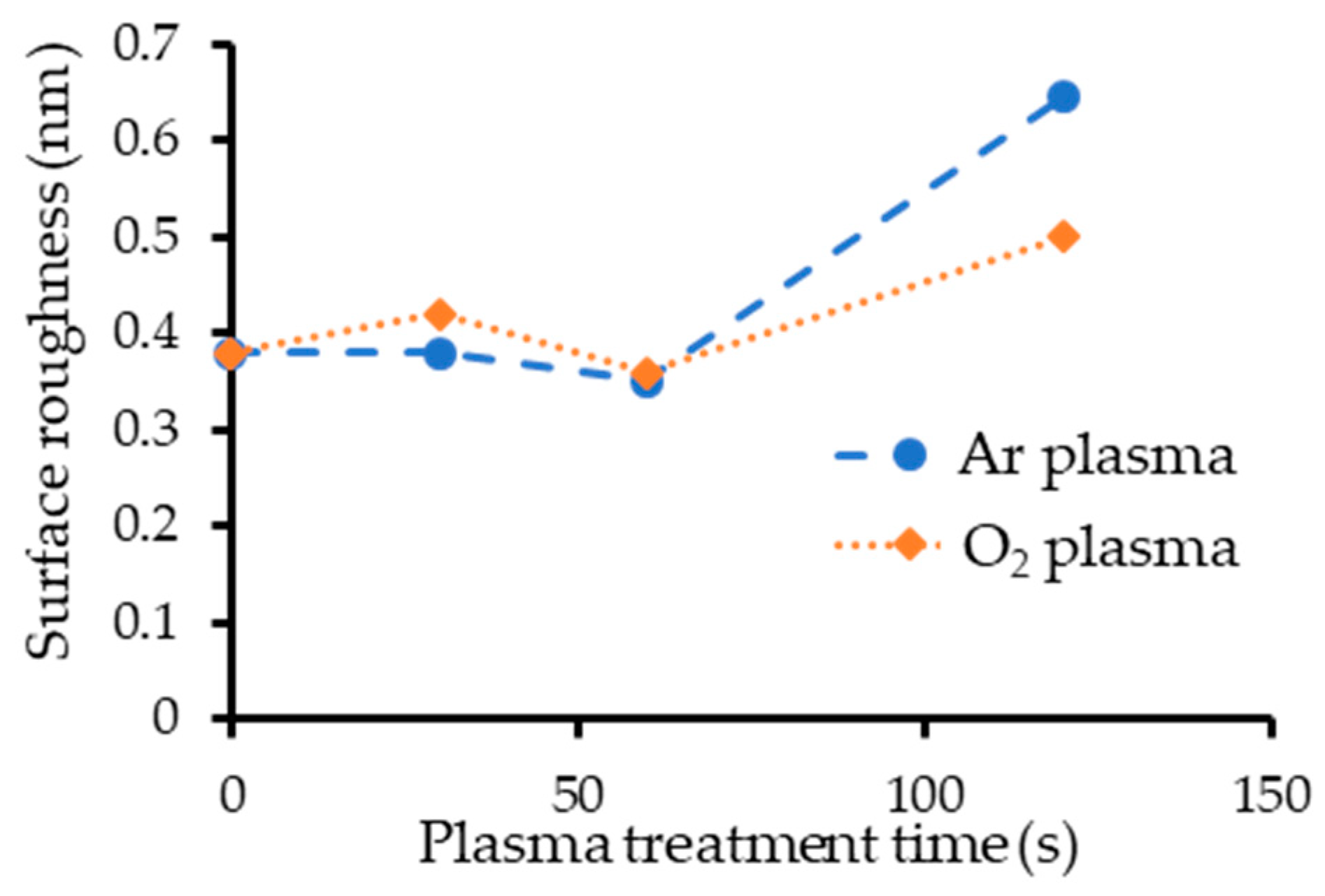
The measured RMS surface roughness for different plasma treatment times (30, 60, 120 s) are plotted in
Figure 1. The roughness before plasma treatment was 0.38 nm. Both the Ar and O
2 plasma treatments of 60 s or less had little effect on surface roughness, while both treatments of 120 s increased it. This indicates that a short plasma treatment time is important for achieving low-temperature bonding.
3.1.2. Contact Angle Measurement
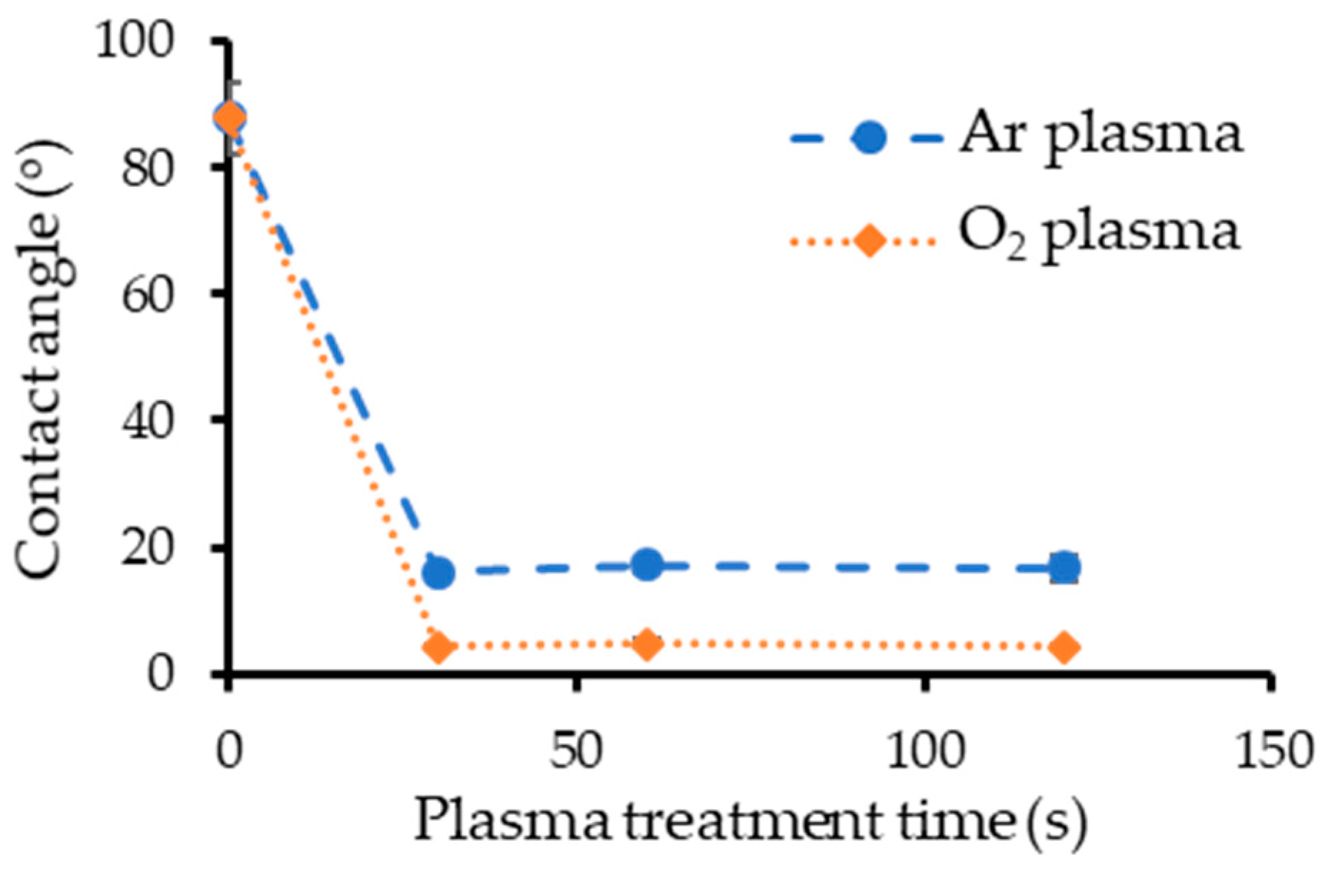
The measured contact angles for different plasma treatment times (30, 60, 120 s) are shown in
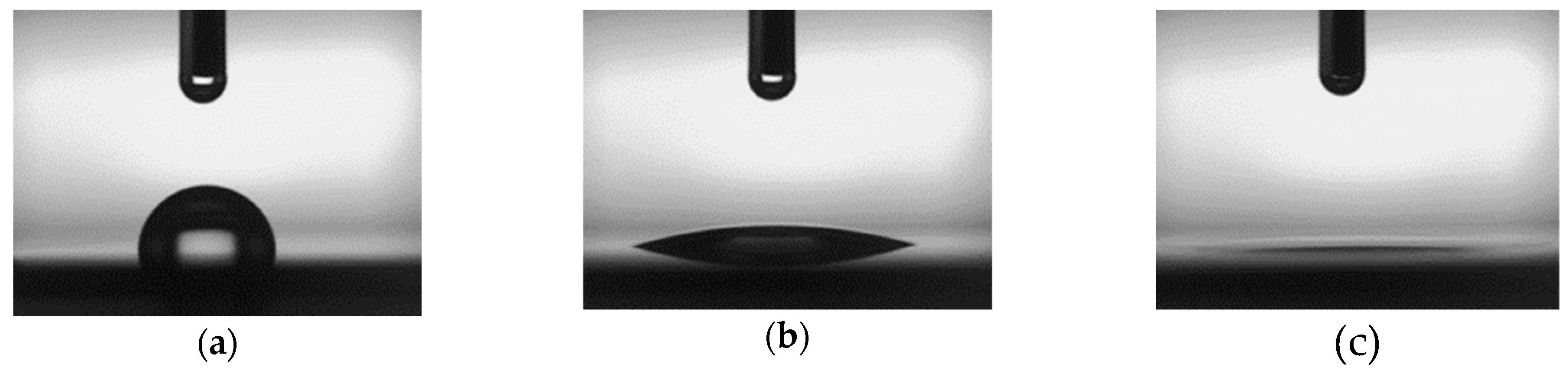
Figure 2. The Au films had been exposed to air for over 1 month, and the measurement was performed immediately after plasma treatment. Typical images of the measured contact angle are shown in
Figure 3.
Figure 3b,c was taken 30 s after plasma treatment. Before treatment, the contact angle was about 80–100°, and the Au surfaces were hydrophobic. Both treatments reduced the contact angle, which means that the Au surfaces became hydrophilic with plasma treatment. The contact angle for Au surfaces with O
2 plasma treatment was less than 5°, which is smaller than that with Ar plasma treatment. The treatment times were the same.
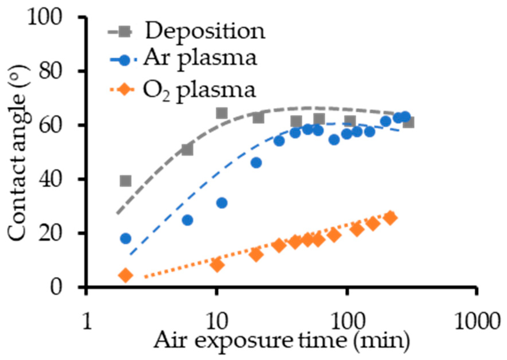
The changes in the contact angle with the air exposure time after Au film deposition and after plasma treatment are plotted in
Figure 4. Previous studies reported that Au film is hydrophilic immediately after deposition and that the Au surface quickly becomes hydrophobic after exposure in air [
32,
33]. The measured change in the contact angle after deposition agrees well with the results of previous studies. The contact angles of Au surfaces that received Ar plasma treatment increased rapidly after exposure in air, similar to the results for the Au film immediately after deposition. In contrast, the rate of increase was much lower for Au surfaces that received O
2 plasma treatment.
3.1.3. Sheet Resistance Measurement
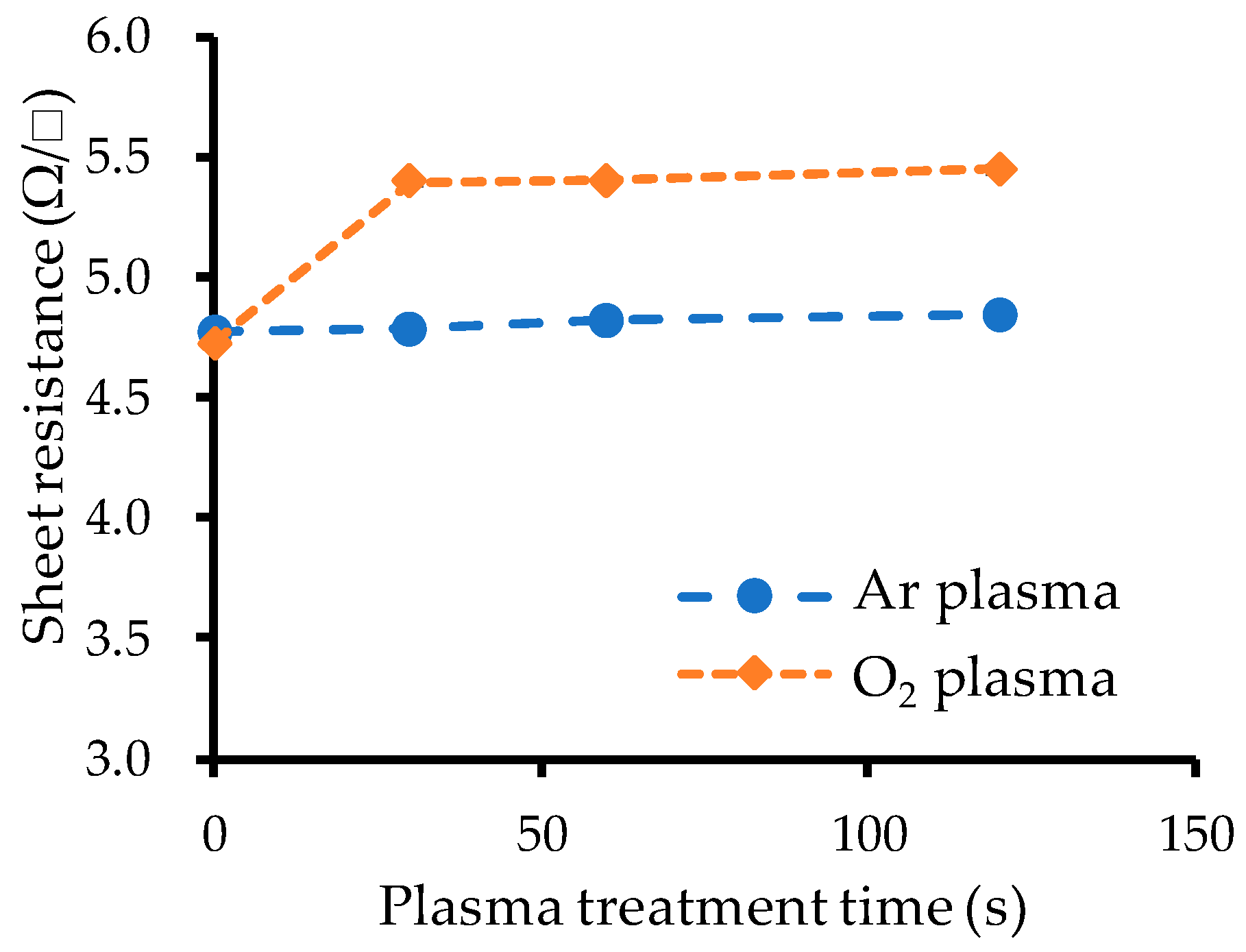
The relationship between the measured sheet resistance and the plasma treatment time is plotted in
Figure 5. Before plasma treatment, the sheet resistance was about 4.7 Ω. While Ar plasma treatment did not change the resistance, 30 s O
2 plasma treatment increased it to about 5.4 Ω. Additional O
2 plasma treatment time did not increase it.
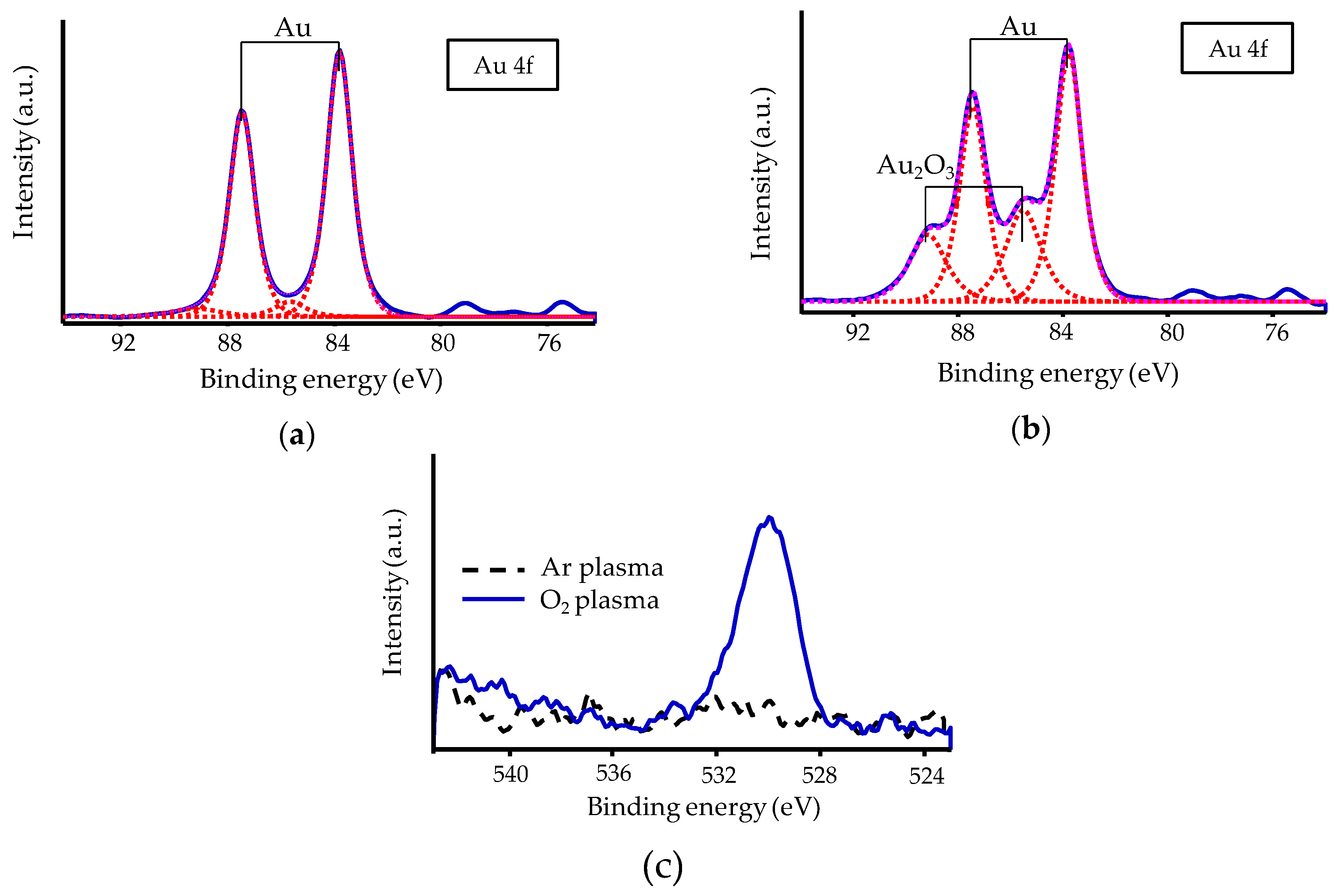
3.1.4. XPS Analysis
The Au surface conditions were evaluated by using XPS analysis to investigate Au surfaces after Ar or O
2 plasma treatment. The treatment time was set to 60 s. The relative peak intensities in the Au 4f region are plotted in
Figure 6a,b, and the relative peak intensities in the O 1s region are plotted in
Figure 6c. The results plotted in (a) show that the Au surfaces that received Ar plasma treatment were pure Au, while those plotted in (b) show that an Au
2O
3 peak appeared for the Au surfaces that received O
2 plasma treatment. The results plotted in (c) show that the O
2 plasma treatment increased the oxygen contamination intensity.
3.1.5. TDS Analysis
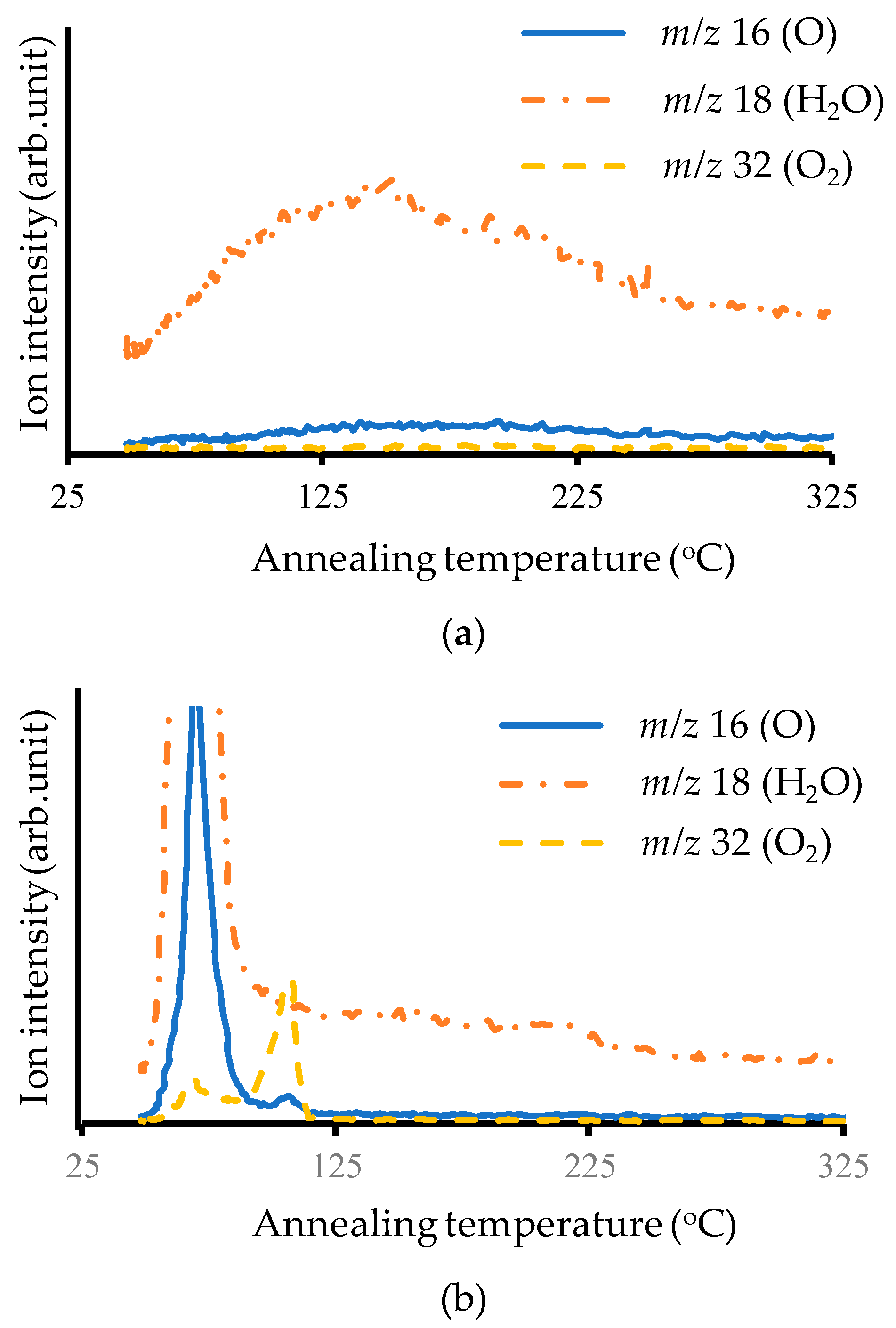
The results of the TDS analysis are plotted in
Figure 7. There was little desorption from the Au surface with the Ar plasma treatment. In contrast, with the O
2 plasma treatment, mass-to-charge ratio (
m/
z) peaks of 16 and 18 were detected at annealing temperatures around 70 °C, and
m/
z peaks of 16 and 32 were detected at annealing temperatures around 110 °C. Since
m/
z 16, 18, and 32 correspond to O, H
2O, and O
2, it appears that H
2O was desorbed around 70 °C from the Au surfaces that received O
2 plasma treatment, while O
2 was desorbed around 110 °C.
3.2. Bonding Results
3.2.1. Effect of Plasma Treatment Time
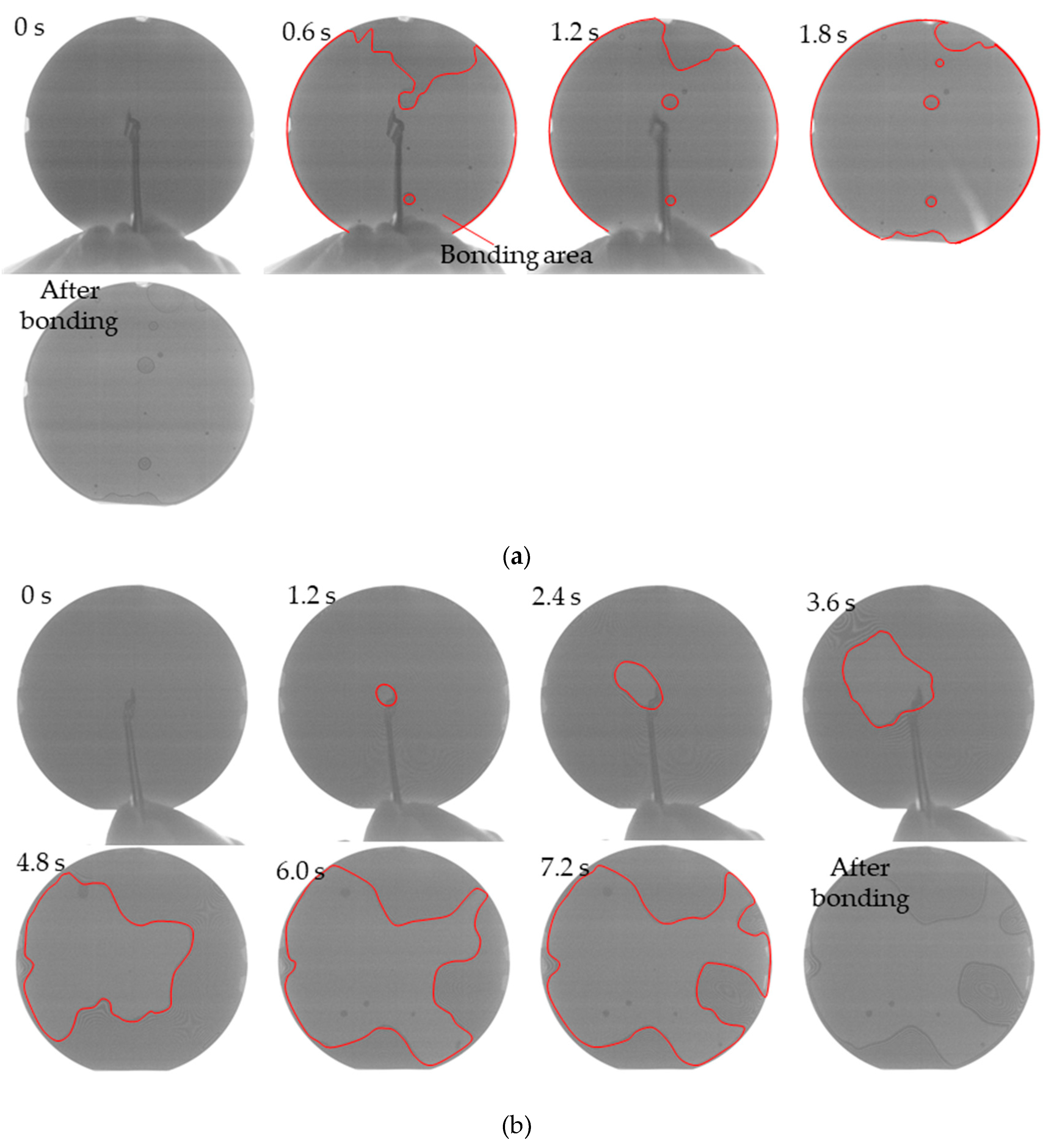
To determine the effect of the plasma treatment time, Au–Au bonding with or without plasma treatment was performed. The treatment times were 30 s or 60 s because a longer treatment time increased the surface roughness. Bonding was performed immediately after plasma treatment. Without plasma treatment, bonding front propagation did not occur, and bonding did not succeed. With plasma treatment, bonding front propagation occurred, and bonding succeeded. IR images of typical bond front propagation between two Si wafers for a plasma treatment time of 60 s are shown in in
Figure 8. The contrast and brightness of the images were adjusted, and the edges of the bonding area were marked to make it more visible. With Ar plasma treatment, the bonding area quickly expanded across the entire 4-inch wafer after pushing the center. With O
2 plasma treatment, the bonding area expanded much more slowly.
The results of the destructive razor blade testing are summarized in
Table 1. With Ar plasma treatment (30 s and 60 s), the bonding was sufficient to break the substrate, meaning that strong bonding was achieved. With O
2 plasma treatment, although much of the area was bonded, the bonding strength (surface energy) was only about 0.1–0.2 J/m
2, lower than the surface energy of Au (1.6 J/m
2) [
34]. Debonding thus occurred between the Au–Au bonding interfaces.
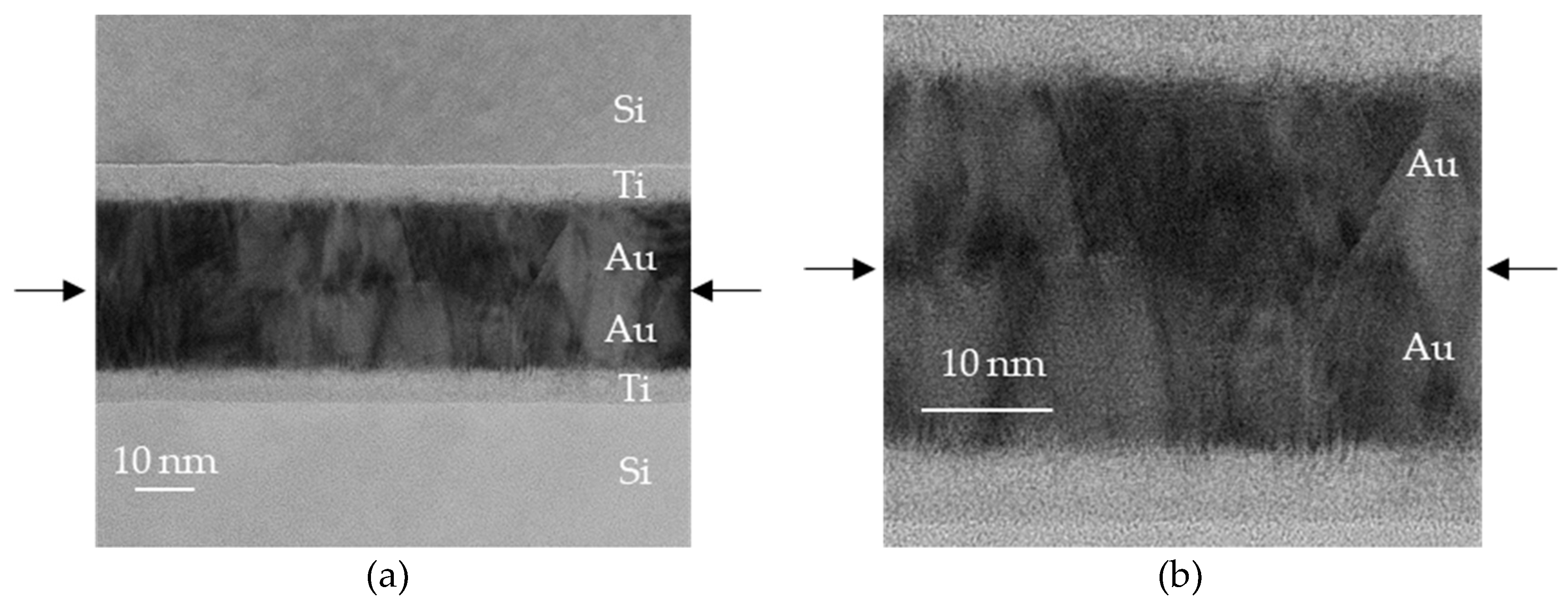
Transmission electron microscope (TEM) images of a bonded sample that received Ar plasma treatment are shown in
Figure 9. Bonding was achieved at the atomic level, and part of the grain boundary grew beyond the bonding interface.
3.2.2. Effect of Air Exposure
To investigate the effect of air exposure after plasma treatment, bonding was performed after air exposure. The bonding of Au films immediately after deposition was also compared. Because Au films immediately after deposition have clean and activated surfaces, bonding can be performed at room temperature. This bonding technique is usually called atomic diffusion bonding [
4,
13,
14]. The effect of air exposure time on the occurrence of self-propagation of the bonding area and on the bonding strength of atomic diffusion bonding for Au films immediately after deposition is summarized in
Table 2. Self-propagation occurred even after 1 h of air exposure. Though the bonding strength decreased as the exposure time increased, sufficient bonding strength (greater than the surface energy of bulk Si (2.5 J/m
2) [
35]) was obtained even after 1 h of air exposure.
The effect of air exposure time for surface activated bonding is summarized in
Table 3. In the cases where self-propagation did not occur, bonding was achieved by pushing the whole wafer with tweezers. With Ar plasma treatment, self-propagation did not occur after 30 min of air exposure. Moreover, the bonding strength greatly decreased as the air exposure time increased. With O
2 plasma treatment, while self-propagation occurred even after 1 hour of air exposure, the bonding strength was lower under all conditions.
3.2.3. Room-Temperature Wafer-Scale Au–Au Bonding After Annealing
Analysis of Au surfaces that received O2 plasma treatment revealed that Au2O3 formed and that O2 desorbed around 110 °C. This indicates that bonding after annealing at over 110 °C increases the bonding strength of samples that receive O2 plasma treatment. Here, annealing up to 150 °C after plasma treatment was investigated: Ar or O2 plasma was irradiated onto Au surfaces for 60 s, and then the wafers were annealed at 150 °C for 10 min in vacuum. After annealing, the wafers were bonded in ambient air at room temperature. The entire annealing process took about one hour.
Self-propagation did not occur in either the Ar or O2 plasma-treated samples. The wafers were thus bonded by pushing the entire wafers with tweezers. Although the bonding strength of samples that received Ar plasma treatment exceeded the surface energy of bulk Si (2.5 J/m2), the annealing reduced the bonding strength, as evidenced by the breaking of the wafers during blade testing for wafers that had not been annealed. The bonding strength of samples that received O2 plasma treatment increased substantially (from 0.1 J/m2 without annealing to 2.5 J/m2 with annealing). To investigate whether Au2O3 was desorbed, XPS analysis of annealed Au surfaces after O2 plasma treatment was also performed. The results did not reveal an Au2O3 peak, meaning that Au2O3 formed by O2 plasma treatment impedes Au–Au bonding. To investigate the change in surface roughness due to annealing, AFM analysis was also performed. The results did not reveal any changes in surface roughness.
4. Discussion
While Ar plasma treatment improved room-temperature wafer-scale Au–Au bonding strength, O2 plasma treatment did not. The O2 plasma treatment reduced the contact angle to less than 5° and increased the sheet resistance. XPS analysis showed that the O2 plasma treatment formed Au2O3 on the Au surface. This indicates that the changes in contact angle and sheet resistance were both apparently caused by oxidation of the Au surfaces and that the Au2O3 formed by the O2 plasma treatment impeded Au–Au bonding.
Because TDS analysis showed that Au2O3 desorbed at around 110 °C, bonding after annealing up to 150 °C was performed. While the bonding strength of samples that received Ar plasma treatment was reduced by the annealing, that of samples that received O2 plasma treatment was improved from 0.1 to 2.5 J/m2. This also demonstrates that the Au2O3 formed by O2 plasma treatment impeded Au–Au bonding. The decrease in bonding strength with Ar plasma treatment may have been due to the annealing processing time (~1 h).
The effects of air exposure after Au film deposition or plasma treatment on the contact angle and bonding strength were also investigated. The changes in surface hydrophilicity due to contact angle measurement of water on Au surfaces that received Ar plasma treatment were similar to those on Au surfaces immediately after deposition. The bonding strength of samples that were exposed in air following Ar plasma treatment decreased more rapidly than that of samples bonded immediately after deposition. Further research on the effects of air exposure and the relationship between surface conditions and bonding strength is necessary.
Previous studies found that O
2 plasma treatment improved Au–Au bonding strength [
23,
24], possibly because Au
2O
3 desorbed due to the high bonding temperature (150 °C) or ultrasonic vibrations.
5. Conclusions
Pretreatment using Ar or O2 plasma was investigated for ambient room-temperature wafer-scale Au–Au bonding using ultrathin Au films. Surface activation by Ar plasma is mainly due to physical etching by Ar ions, while surface activation by O2 plasma is mainly due to chemical reaction. The O2 plasma treatment increased the sheet resistance of the Au surfaces but did not increase the bonding strength. XPS analysis revealed that Au2O3 formed on the Au surfaces that received O2 plasma treatment, and TDS analysis revealed that annealing at over 110 °C is necessary for desorption of Au2O3. Annealing up to 150 °C before bonding increased the bonding strength of samples that received O2 plasma treatment, demonstrating that Au2O3 impedes strong Au–Au bonding.
On the other hand, Ar plasma treatment increased the Au–Au bonding strength enough for the Si substrate to be broken in destructive razor blade testing. Although an Au surface that receives Ar plasma treatment is more activated than one that receives O2 plasma treatment, bonding should be performed immediately after plasma treatment.
Author Contributions
Investigation, M.Y., T.M., Y.K., H.T., T.S., T.I. and E.H.; Methodology, M.Y. and E.H.; Validation, M.Y.; Data curation, M.Y.; Writing—original draft, M.Y.; Writing—review & Editing, T.M., Y.K., H.T., T.S., T.I. and E.H.; Funding acquisition, T.H. and E.H.; Resource, H.T., T.S., T.I. and E.H.; Supervision, T.S., T.I. and E.H.; Project administration, E.H.
Funding
This work is partly supported by New Energy and Industrial Technology Development Organization (NEDO).
Conflicts of Interest
The authors declare no conflict of interest.
References
- Morrow, P.R.; Park, C.-M.; Ramanathan, S.; Kobrinsky, M.J.; Harmes, M. Three-dimensional wafer stacking via Cu-Cu bonding integrated with 65-nm strained-Si/low-k CMOS technology. IEEE Electron Device Lett. 2006, 27, 335–337. [Google Scholar] [CrossRef]
- Higurashi, E. Low-temperature bonding technologies for photonics applications. ECS Trans. 2013, 50, 351–362. [Google Scholar] [CrossRef]
- Howlader, M.M.R.; Okada, H.; Kim, T.H.; Itoh, T.; Suga, T. Wafer level surface activated bonding tool for MEMS packaging. J. Electrochem. Soc. 2004, 151, G461. [Google Scholar] [CrossRef]
- Shimatsu, T.; Uomoto, M. Atomic diffusion bonding of wafers with thin nanocrystalline metal films. J. Vac. Sci. Technol. B Nanotechnol. Microelectron. Mater. Process. Meas. Phenom. 2010, 28, 706–714. [Google Scholar] [CrossRef]
- Niklaus, F.; Stemme, G.; Lu, J.-Q.; Gutmann, R.J. Adhesive wafer bonding. J. Appl. Phys. 2006, 99, 031101. [Google Scholar] [CrossRef]
- Andrijasevic, D.; Austerer, M.; Andrews, A.M.; Klang, P.; Schrenk, W.; Strasser, G. Hybrid integration of GaAs quantum cascade lasers with Si substrates by thermocompression bonding. Appl. Phys. Lett. 2008, 92, 10–13. [Google Scholar] [CrossRef]
- Taklo, M.M.V.; Storås, P.; Schjølberg-Henriksen, K.; Hasting, H.K.; Jakobsen, H. Strong, high-yield and low-temperature thermocompression silicon wafer-level bonding with gold. J. Micromechanics Microengineering 2004, 14, 884–890. [Google Scholar] [CrossRef]
- Tanida, K.; Umemoto, M.; Morifuji, T.; Kajiwara, R.; Ando, T.; Tomita, Y.; Tanaka, N.; Takahashi, K. Au Bump Interconnection in 20 µm Pitch on 3D Chip Stacking Technology. Jpn. J. Appl. Phys. 2003, 42, 6390–6395. [Google Scholar] [CrossRef]
- Unami, N.; Sakuma, K.; Mizuno, J.; Shoji, S. Effects of excimer irradiation treatment on thermocompression Au-Au bonding. Jpn. J. Appl. Phys. 2010, 49, 10–13. [Google Scholar] [CrossRef]
- Zhang, G.G.; Ang, X.F.; Chen, Z.; Wong, C.C.; Wei, J. Critical temperatures in thermocompression gold stud bonding. J. Appl. Phys. 2007, 102, 063519. [Google Scholar] [CrossRef]
- Jing, E.; Xiong, B.; Wang, Y. Low-temperature Au–Si wafer bonding. J. Micromechanics Microengineering 2010, 20, 095014. [Google Scholar] [CrossRef]
- Al Farisi, M.S.; Hirano, H.; Frömel, J.; Tanaka, S. Wafer-level hermetic thermo-compression bonding using electroplated gold sealing frame planarized by fly-cutting. J. Micromechanics Microengineering 2017, 27, 015029. [Google Scholar] [CrossRef]
- Shimatsu, T.; Uomoto, M.; Kon, H. Room Temperature Bonding Using Thin Metal Films (Bonding Energy and Technical Potential). ECS Trans. 2014, 64, 317–328. [Google Scholar] [CrossRef]
- Uomoto, M.; Shimatsu, T. Necessary Thickness of Au Capping Layers for Room Temperature Bonding of Wafers in Air Using Thin Metal Films with Au Capping Layers. ECS Trans. 2016, 75, 67–76. [Google Scholar] [CrossRef]
- Higurashi, E.; Imamura, T.; Suga, T.; Sawada, R. Low-temperature bonding of laser diode chips on silicon substrates using plasma activation of Au films. IEEE Photonics Technol. Lett. 2007, 19, 1994–1996. [Google Scholar] [CrossRef]
- Kurashima, Y.; Maeda, A.; Takagi, H. Room-temperature wafer scale bonding using smoothed Au seal ring surfaces for hermetic sealing. Jpn. J. Appl. Phys. 2016, 55, 016701. [Google Scholar] [CrossRef]
- Higurashi, E.; Okumura, K.; Kunimune, Y.; Suga, T.; Hagiwara, K. Room-Temperature Bonding of Wafers with Smooth Au Thin Films in Ambient Air Using a Surface-Activated Bonding Method. IEICE Trans. Electron. 2017, E100–C, 156–160. [Google Scholar] [CrossRef]
- Matsumae, T.; Kurashima, Y.; Takagi, H. Surface activated bonding of Ti/Au and Ti/Pt/Au films after vacuum annealing for MEMS packaging. Microelectron. Eng. 2018, 197, 76–82. [Google Scholar] [CrossRef]
- Matsumae, T.; Kurashima, Y.; Umezawa, H.; Mokuno, Y.; Takagi, H. Room-temperature bonding of single-crystal diamond and Si using Au/Au atomic diffusion bonding in atmospheric air. Microelectron. Eng. 2018, 195, 68–73. [Google Scholar] [CrossRef]
- Bond, G.C. Gold: A relatively new catalyst. Gold Bull. 2001, 34, 117–119. [Google Scholar] [CrossRef] [Green Version]
- Raiber, K.; Terfort, A.; Benndorf, C.; Krings, N.; Strehblow, H.-H. Removal of self-assembled monolayers of alkanethiolates on gold by plasma cleaning. Surf. Sci. 2005, 595, 56–63. [Google Scholar] [CrossRef]
- Hook, D.A.; Olhausen, J.A.; Krim, J.; Dugger, M.T. Evaluation of Oxygen Plasma and UV Ozone Methods for Cleaning of Occluded Areas in MEMS Devices. J. Microelectromechanical Syst. 2010, 19, 1292–1298. [Google Scholar] [CrossRef]
- Peng, H.Y.; Devarajan, M.; Lee, T.T. Comparison of Argon and Oxygen Plasma Treatments on LED Chip Bond Pad for Wire Bond Application. Int. J. Sci. Eng. Res. 2014, 5, 908–912. [Google Scholar]
- Peng, H.Y.; Devarajan, M.; Lee, T.T.; Lacey, D. Investigation of oxygen followed by argon plasma treatment on LED chip bond pad for wire bond application. Solder. Surf. Mt. Technol. 2015, 27, 129–136. [Google Scholar] [CrossRef]
- Yamamoto, M.; Higurashi, E.; Suga, T.; Sawada, R.; Itoh, T. Properties of various plasma surface treatments for low-temperature Au–Au bonding. Jpn. J. Appl. Phys. 2018, 57, 04FC12. [Google Scholar] [CrossRef] [Green Version]
- Koo, J.-M.; Lee, J.-B.; Moon, Y.; Moon, W.-C.; Jung, S.-B. Atmospheric pressure plasma cleaning of gold flip chip bump for ultrasonic flip chip bonding. J. Phys. Conf. Ser. 2008, 100, 012034. [Google Scholar] [CrossRef] [Green Version]
- Maszara, W.P.; Goetz, G.; Caviglia, A.; McKitterick, J.B. Bonding of silicon wafers for silicon-on-insulator. J. Appl. Phys. 1988, 64, 4943–4950. [Google Scholar] [CrossRef]
- Vallin, Ö.; Jonsson, K.; Lindberg, U. Adhesion quantification methods for wafer bonding. Mater. Sci. Eng. R Reports 2005, 50, 109–165. [Google Scholar] [CrossRef]
- Brantley, W.A. Calculated elastic constants for stress problems associated with semiconductor devices. J. Appl. Phys. 1973, 44, 534–535. [Google Scholar] [CrossRef]
- Fournel, F.; Continni, L.; Morales, C.; Da Fonseca, J.; Moriceau, H.; Rieutord, F.; Barthelemy, A.; Radu, I. Measurement of bonding energy in an anhydrous nitrogen atmosphere and its application to silicon direct bonding technology. J. Appl. Phys. 2012, 111, 104907. [Google Scholar] [CrossRef]
- Bagdahn, J.; Petzold, M.; Reiche, M.; Gutjahr, K. Characterization of directly bonded silicon wafers by means of the double cantilever crack opening method. In Proceedings of the Fourth International Symposium on Semiconductor Wafer Bonding: Science, Technology, and Applications, Electrochemical Society Proceedings Vol. PV97, Paris, France, 30 August–5 September 1997; Volume 36, pp. 291–298. [Google Scholar]
- Smith, T. The hydrophilic nature of a clean gold surface. J. Colloid Interface Sci. 1980, 75, 51–55. [Google Scholar] [CrossRef]
- Zhu, J.; Zangari, G.; Reed, M.L. Tailoring the wetting properties of surface-modified nanostructured gold films. J. Phys. Chem. C 2011, 115, 17097–17101. [Google Scholar] [CrossRef]
- Mezey, L.Z.; Giber, J. The surface free energies of solid chemical elements: Calculation from internal free enthalpies of atomization. Jpn. J. Appl. Phys. 1982, 21, 1569–1571. [Google Scholar] [CrossRef]
- Tong, Q.-Y.; Kim, W.J.; Lee, T.-H.; Gösele, U. Low vacuum wafer bonding. Electrochem. Solid-State Lett. 1999, 1, 52. [Google Scholar] [CrossRef]
© 2019 by the authors. Licensee MDPI, Basel, Switzerland. This article is an open access article distributed under the terms and conditions of the Creative Commons Attribution (CC BY) license (http://creativecommons.org/licenses/by/4.0/).

 ,
, 


