Article

PCB-YOLO: An Improved Detection Algorithm of PCB Surface Defects Based on YOLOv5

1
School of Physics and Electronic Science, Changsha University of Science and Technology, Changsha 410114, China
2
School of Computer and Communications Engineering, Changsha University of Science and Technology, Changsha 410114, China
*
Author to whom correspondence should be addressed.
Sustainability 2023, 15(7), 5963; https://doi.org/10.3390/su15075963
Submission received: 1 March 2023 / Revised: 23 March 2023 / Accepted: 27 March 2023 / Published: 29 March 2023

Abstract

:
To address the problems of low network accuracy, slow speed, and a large number of model parameters in printed circuit board (PCB) defect detection, an improved detection algorithm of PCB surface defects based on YOLOv5 is proposed, named PCB-YOLO, in this paper. Based on the K-means++ algorithm, more suitable anchors for the dataset are obtained, and a small target detection layer is added to make the PCB-YOLO pay attention to more small target information. Swin transformer is embedded into the backbone network, and a united attention mechanism is constructed to reduce the interference between the background and defects in the image, and the analysis ability of the network is improved. Model volume compression is achieved by introducing depth-wise separable convolution. The EIoU loss function is used to optimize the regression process of the prediction frame and detection frame, which enhances the localization ability of small targets. The experimental results show that PCB-YOLO achieves a satisfactory balance between performance and consumption, reaching 95.97% mAP at 92.5 FPS, which is more accurate and faster than many other algorithms for real-time and high-precision detection of product surface defects.

1. Introduction

With the development of the electronics industry, the electronics industry occupies an important position in the modern manufacturing industry. As an important electronic component, the printed circuit board (PCB) is a carrier connected to various electronic components that provides line connections and hardware support for the equipment. From small electronic watches and calculators to large computers, communication electronics, and military weapons systems, as long as there are electronic components such as integrated circuits, almost every electronic device needs a PCB [1,2,3,4]. However, the PCB manufacturing process is complex and prone to miss holes, mouse bites, open circuits, shorts, and other minor defects. To ensure the safety and reliability of electronic equipment, it is necessary to detect the surface defects of PCB.
Traditional manual inspection is easily disrupted by external environmental factors, which can affect the efficiency of defect detection. Additionally, the detection of tiny defects can cause visual fatigue and lead to misclassification [5]. To solve the problems, some scholars have introduced machine learning into PCB detection and have made great progress. Wang et al. [6] proposed an automatic detection algorithm for PCB pinholes by combining machine learning knowledge. Pinhole defects of 2 mm can be identified within 10 s. Yuk et al. [7] implemented the detection of PCB defects using accelerated robust features and random forest algorithm. Weighted kernel density estimation (WKDE) mappings were generated with weighted probabilities by considering the density of features to achieve the detection of defect concentration regions. V et al. [8] used similarity metrics for the detection of PCB surface defects. Experimental results demonstrated the effectiveness of this method in detecting and locating local defects in PCB images of complex component installations. Some scholars have also proposed PCB surface defect detection approaches based on machine learning, which are not real-time approaches [9,10]. Although machine learning-based methods can achieve recognition of PCB surface defects, most algorithms still require the artificial setting of image features through a priori knowledge, which results in the algorithms’ lack of generalization ability.
Traditional image processing-based defect detection methods achieve acceptable detection accuracy; however, they are time-consuming and sensitive to the environment and inferred images [11]. With the development of deep learning (DL) and computer vision, DL and convolutional neural network (CNN) techniques are widely used in the detection of PCB defects. The existing deep learning target detection methods are mainly divided into the single-stage and the two-stage detection algorithm. The single-stage algorithm processes the entire input image in a single pass to detect objects. These algorithms typically use a single CNN to perform both the region proposal and object detection. The two-stage algorithm separates the object proposal from object detection. The first stage of a two-stage algorithm generates region proposals using a separate algorithm or network; then, the second stage performs object detection within those proposed regions. The two-stage detection algorithm is represented by R-CNN (regions with CNN features) [12], Fast R-CNN (fast region-based CNN) [13], and Faster R-CNN [14]. These algorithms were used to generate candidate boxes and then classify each candidate box. The single-stage detection algorithm is represented by the YOLO (You Only Look Once) series [15,16,17,18] and SSD (Single Shot MultiBox Detector) [19]. These algorithms directly generated the class probability and position coordinate values of the object while creating the candidate frame, and the final detection results can be directly obtained after a single detection. To address the problem that image uncertainty can limit PCB detection performance under uneven ambient light or unstable transmission channels, Yu et al. [20] designed a novel collaborative learning classification model. Zhang et al. [21] obtained a good detection effect by using a cost-sensitive residual convolutional neural network for PCB appearance defects; however, the model has high complexity and a large number of parameters. Wan et al. [22] achieved the detection of PCB surface defects by using a few labeled samples based on semi-supervised learning (SSL) methods, which improved the detection efficiency with a detection mean average precision (mAP) of 98.4%. Ding et al. [23] proposed TDD-net (tiny defect detection) based on Faster R-CNN for the detection of tiny target defects in PCB. The accuracy is high but the model size is too large to be used on embedded devices. Xuan et al. [24] proposed a detection algorithm based on YOLOX and coordinate attention for PCB defects detection, which has good robustness; however, the size of the algorithm model is 379 MB. Wu et al. [25] proposed the GSC YOLOv5, a deep learning detection method that incorporates lightweight networks and a dual-attention mechanism, to effectively solve the small target detection problem; however, the proposed attention mechanism is complex and slow. Zheng et al. [26] implemented real-time detection of PCB surface defects based on MobileNet-V2. The mAP of four types of defects is only 92.86%, which needs to continue to improve. Yu et al. [27] proposed the diagonal feature pyramid (DFP) to improve the performance of tiny defect detection. However, the model size is 69.3MB and still needs further quantification. Other scholars have also proposed a series of detection methods based on deep learning techniques, all of which have problems of large model size and poor real-time performance [28,29].
Deep learning-based detection algorithms have been able to achieve good accuracy in other defect detection fields. In industrial applications, as PCB surface defect detection requires high accuracy and real-time performance, the current PCB surface defect detection algorithm needs to be further improved in terms of detection accuracy and speed. Therefore, in order to further improve the model accuracy, a real-time detection network based on the YOLOv5 algorithm is designed, which provides theoretical support for the subsequent deployment of the embedded platform. Specific innovation points are as follows:
(1)
The K-means ++ algorithm was used to obtain 12 new sets of anchors, which solves the problem that YOLOv5 preset anchors based on the COCO dataset are not applicable to the PCB dataset. Based on the new anchors, a new detection layer is added to obtain more information about the features of the target.
(2)
A united attention mechanism is designed by combining the channel attention module and the spatial attention module. It pays better attention to the channel information and spatial information of the features.
(3)
Combined with the Swin transformer and depth-wise separable convolution, a backbone network is designed for feature extraction. More spatial and channel information are obtained, and the analysis capability of the network is improved.
(4)
During the training process, the CIoU(Complete-IoU) [30] is replaced by the regression loss function EIoU(Efficient-IoU) [31], which more clearly measures the differences in the overlap area, centroids, and edge lengths in the bounding box regression. The convergence speed of the model is accelerated and the model regression accuracy is improved.
The remainder of this paper is organized as follows. Section 2 introduces the image preprocessing and dataset. Section 3 presents the details of the proposed method. Section 4 reports the experimental results and discussion. Section 5 concludes this article and considers further work.

2. Image Preprocessing and Dataset

The original PCB defect dataset was obtained from the Intelligent Robot Development Laboratory of Peking University [
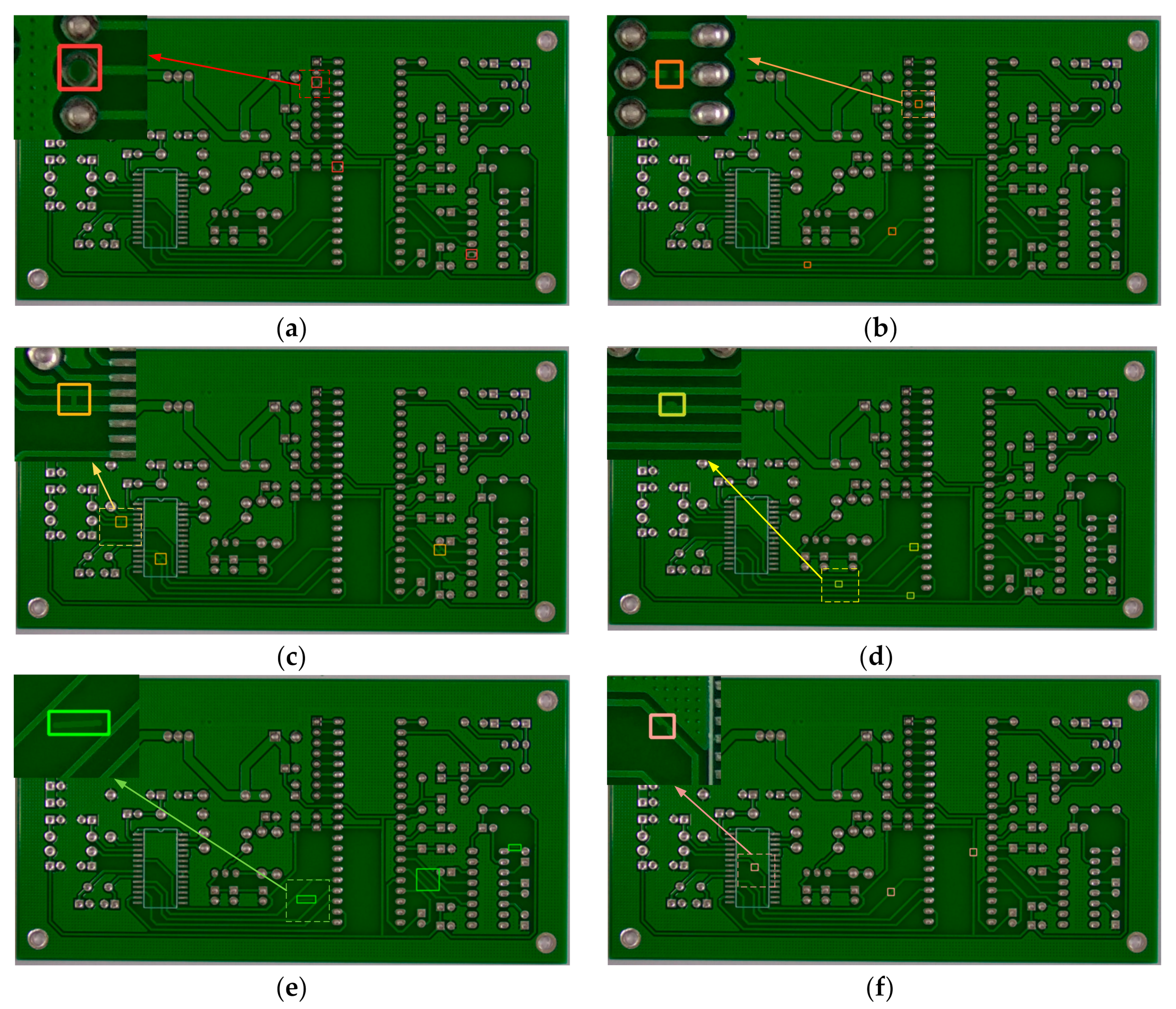
23]. For this dataset, the average pixel size of each image is 2777 × 2138, and the average pixel size of the six defects is 130 × 110. There are a total of 1386 images with six types of defects, which are short, spur, open circuit, mouse bite, spurious copper, missing hole, and various defects are shown in 
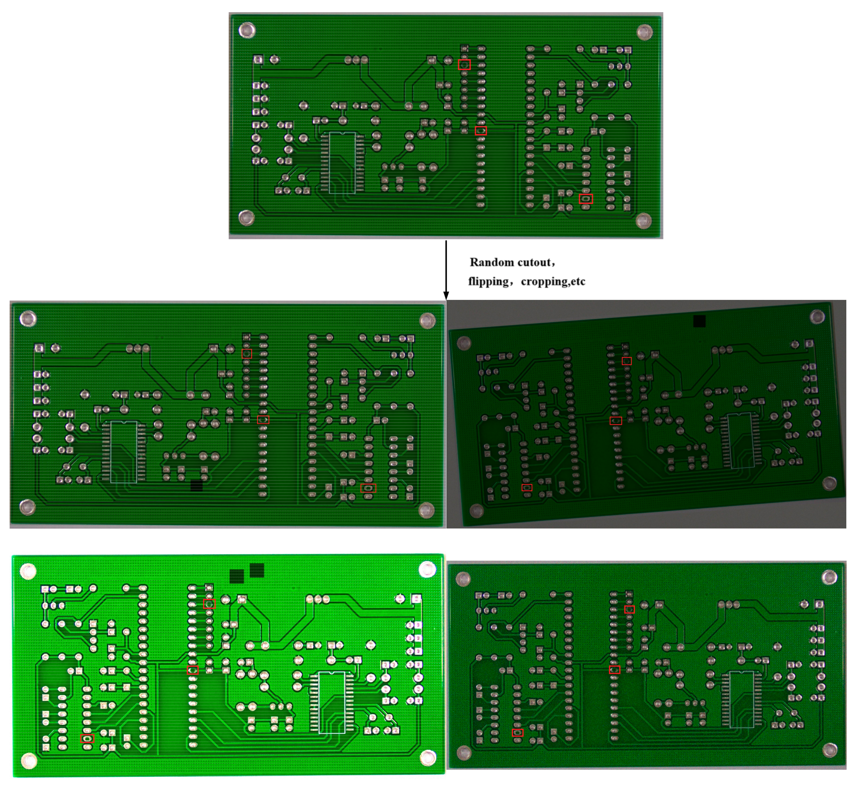
Figure 1. Due to the small number of samples in the original dataset, problems such as low detection accuracy, low robustness, and overfitting are likely to occur in the training process. The problem of insufficient training samples can be effectively solved by appropriately enhancing the original image to increase the number of images [32]. More and richer training data can be generated through various transformations of the image, which can effectively avoid overfitting and improve the generalization ability of the model. In this paper, the dataset was extended to 8316 images after the random flipping, rotation, cropping, and cutout operations in Figure 2, where the ratio of the training set, validation set, and test set is 8:1:1, and the number of each defect image in the dataset is shown in Table 1. A comparison of original and enhanced dataset is shown in Table 2; the mAP is increased from 90.56% to 93.88%.

3. Description of Methodology

3.1. PCB-YOLO Network Structure

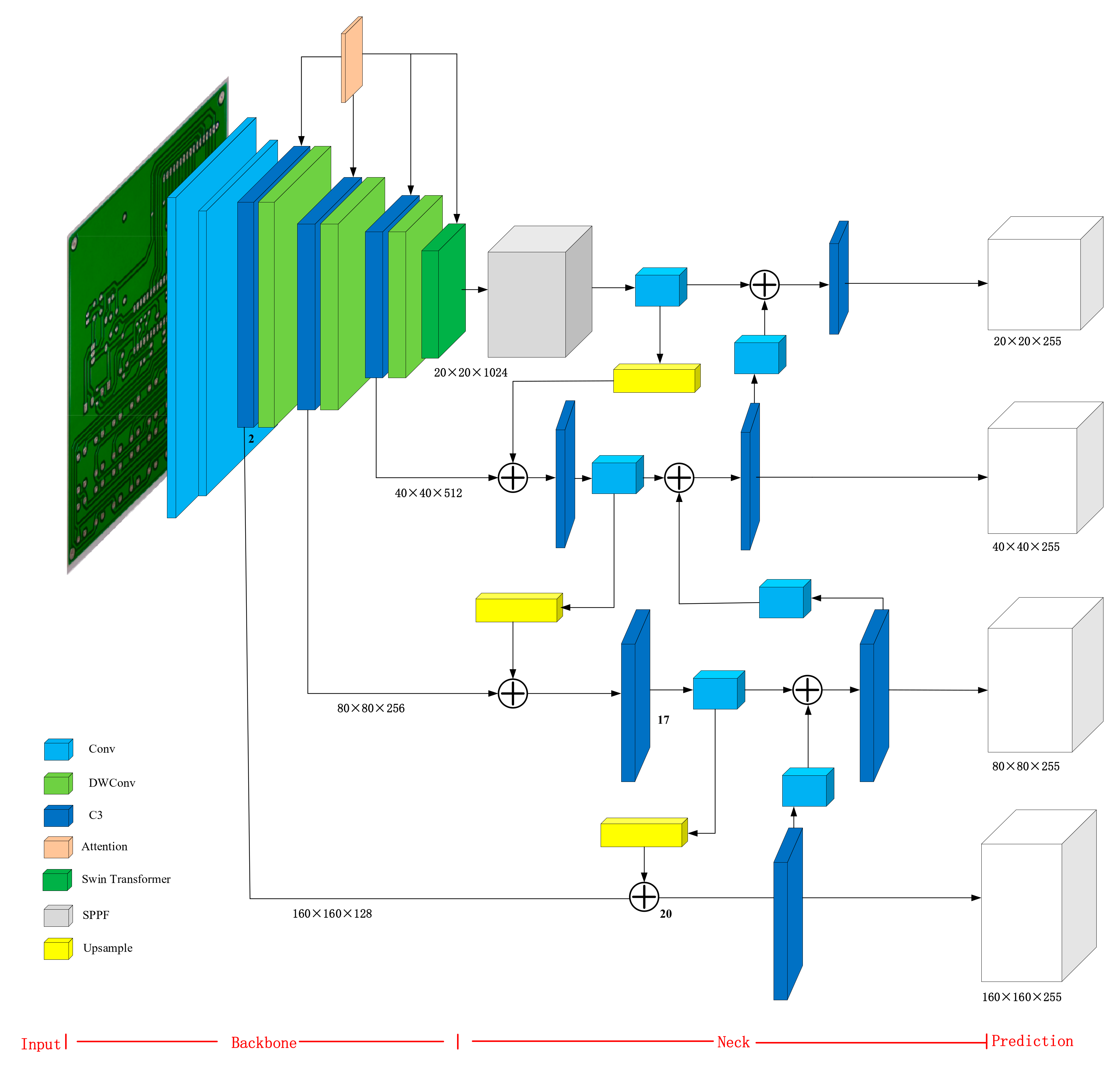
In this study, improvements are made based on the three basic structural frameworks of the spine, neck and head of YOLOv5. YOLOv5 extracts three networks with different levels of scale feature maps for detection, (80,80), (40,40), and (20,20). In order to obtain more information about the features of the small target to be detected, a new detection layer is added according to the new anchors obtained using the K-means++ algorithm.
Figure 3 shows that the PCB-YOLO network structure consists of four parts: input, backbone, neck, and prediction. In input, the image is adjusted to 640 × 640 × 3 and input to the backbone. The united attention mechanism and Swin transformer module are embedded in the backbone to improve the model’s ability to pay attention to channel information and spatial information. DwConv is used to compress the model, which not only guarantees the accuracy of the model but also greatly reduces the size of the model. The network at different levels of four scale feature maps are extracted for detection, which were (160,160), (80,80), (40,40), (20,20) respectively.
In the dataset, the average pixel size of each image is 2777 × 2138 and the pixels of the six defects are 130 × 110. According to the definition in the literature [33], the types of detects of PCB with less than 1.23% of annotated pixels are small objects. In order to solve the problem of YOLOv5 preset anchors based on the COCO dataset not being applicable to PCB datasets, this paper uses the K-means++ algorithm to generate 12 new sets of anchors. A sample point is randomly selected from the uniformly distributed small target PCB dataset X as the first initial clustering center C 1 . The shortest distance D x i is calculated from each sample x i and the current clustering center C 1 , to the probability P x i of each sample x i being selected as the next clustering center is calculated, P x i is represented by Equation (1). The K = 12 clustering centers ( C 1   C k ) are selected according to the roulette wheel method. The distance D x i is calculated from each sample x i to K = 12 clustering centers in the PCB dataset X , and the sample x i is divided into the category C i corresponding to the clustering center with the smallest distance D x i . The clustering center E is recalculated for each category C i , and E is represented by Equation (2), until the position of the clustering center C k no longer changes. Equation (3) is the clustering means.
P ( x ) = D ( x ) 2 x X D ( x ) 2
E = i = 1 k x C i x μ i 2 2
μ i = 1 | C i | x C i x
where X is PCB dataset, C is the cluster center, P is the probability of the cluster center, and D is the shortest distance from sample x to the cluster center C . E is the new cluster center.
Finally, 12 new sets of anchors, (7,7) (11,11) (13,13) (11,18) (17,12) (16,16) (13,24) (24,13) (20,20) (35,13) (28,23) (36,34), are obtained using the K-means++ algorithm. A new small target detection layer is added according to the new anchors. In the new small target detection layer, the feature map 80 × 80 × 256 is up-sampled and further expanded to 160 × 160 × 128 by other processes. In addition, the feature map 160 × 160 × 128 in the bone network is concatenated and fused to obtain a larger feature map 160 × 160 × 255 for small target detection.

3.2. Bakbone Network

3.2.1. United Attention Mechanism

The attention mechanism essentially locates interesting information and suppresses useless information. The PCB dataset contains complex background information. After feature extraction of the convolutional layer, the defect information to be detected takes up a small proportion, while the background and non-detected object information takes up a large proportion. This non-interest region information will interfere with defect detection.
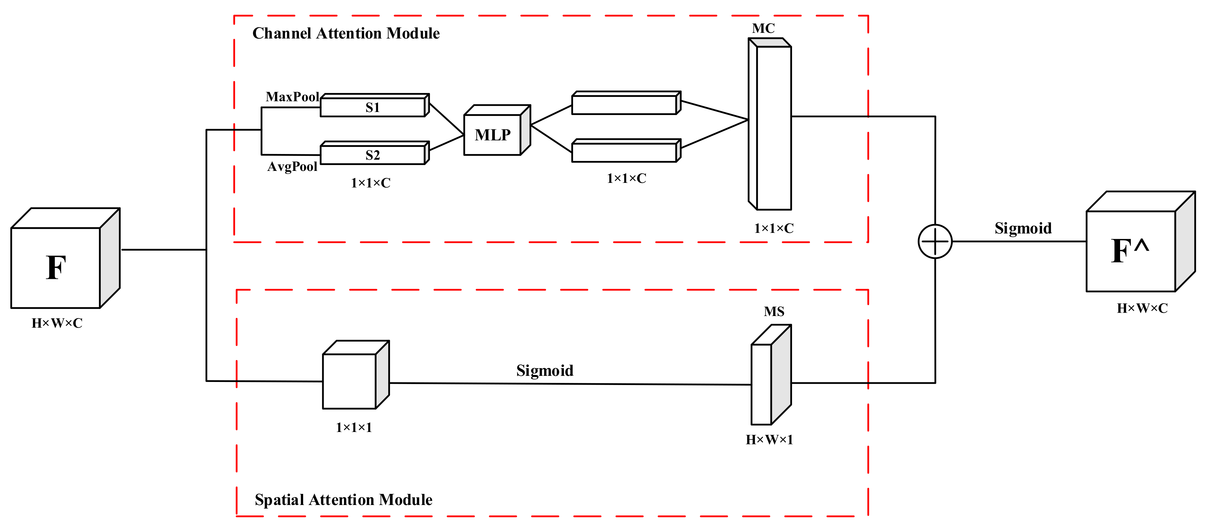
In order to focus on the defect target to be detected in the image and ignore the irrelevant object information, a united attention mechanism (UAM) is design based on the channel attention module (CAM) and spatial attention module (SAM) proposed by Woo et al. [34]. The UAM consists of channel attention module and spatial attention module connected in parallel. Through the parallel structure, the feature map information about both spatial dimensions and channel dimensions is encoded simultaneously, which can make better use of the information between the channel and space of the feature map. The detailed structure of the UAM is shown in Figure 4, where F is the input of the feature map, H and W are the height and width, respectively, and C is number of channels of the input of feature map. In CAM, the global space information of F is firstly compressed using max pool and avg pool to generate two feature maps S1 and S2 of size 1 × 1 × C. Then, two one-dimensional feature maps are obtained through multi-layer perception (MLP). The two one-dimensional feature maps are normalized to obtain the weighted feature map MC. In SAM, the result is input into the sigmoid function after F is activated by the 1 × 1 × 1 convolutional module to obtain the weight feature graph MS. The MC and MS are connected in parallel by element-by-element summation, and the output feature map F^ is obtained after the sigmoid activation function is executed.

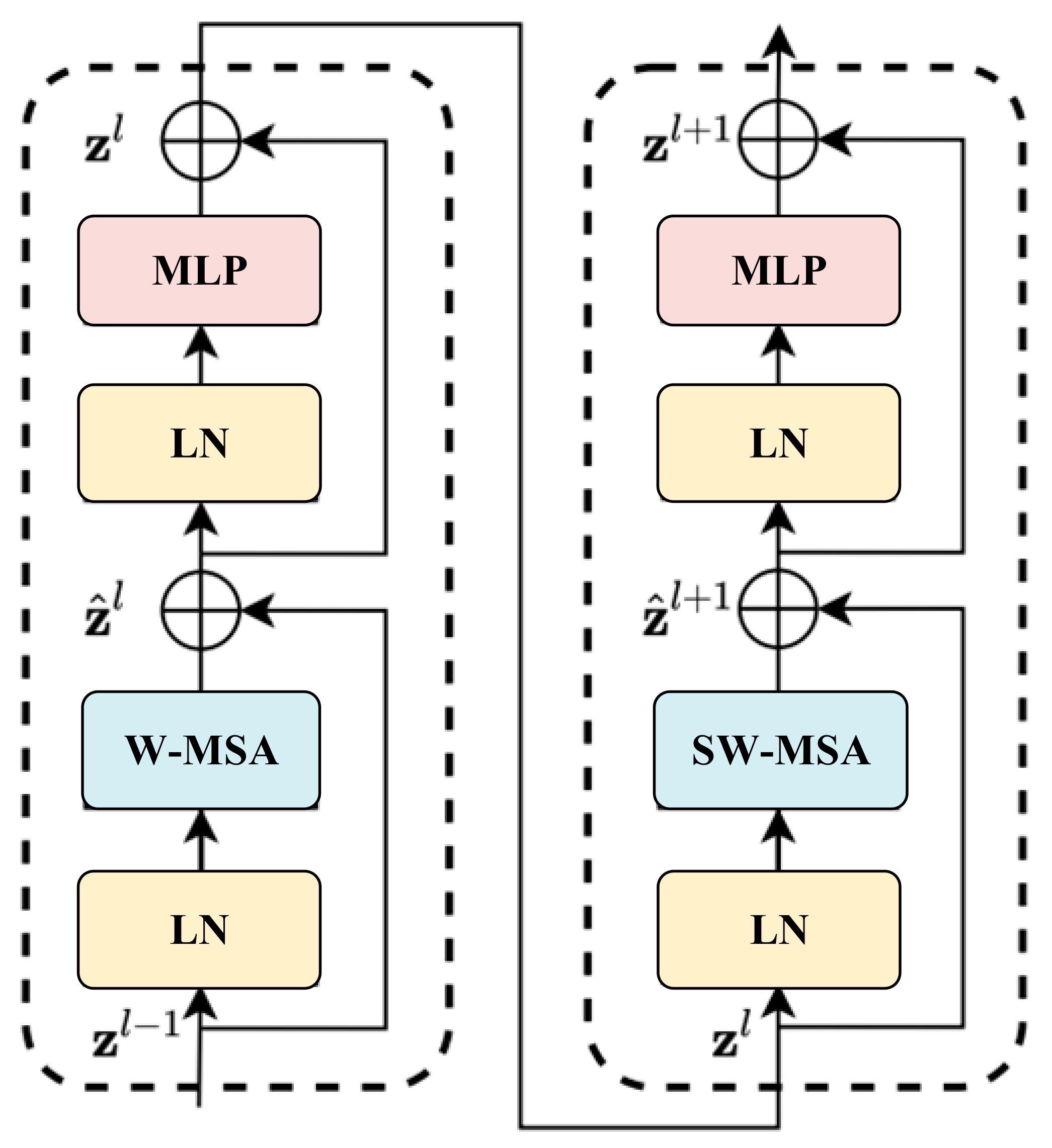
3.2.2. Swin Transformer Module

The transformer is a model based on a self-attentive mechanism, which not only has strong modeling function in the global environment but also shows excellent transferability for downstream tasks under large-scale pre-training. VIT [35] was the first transformer for computer vision, and its demonstrated powerful performance in image classification has driven the development of subsequent transformers for computer vision. The Swin transformer proposed by Liu et al. [36] is the most popular hierarchical vision transformer that is able to compute attention within a local window without overlap, and allows cross-window computation by introducing shift windows. The Swin transformer overcomes the lack of connectivity between the windows generated by the conventional window partitioning strategy in VIT, which leads to higher efficiency and lower complexity.
The structure of the Swin transformer is shown in Figure 5, which consists of two shifted windowing-based self-attention mechanisms and two MLPs. Each self-attention mechanism module and MLP module is preceded by an LN (LayerNorm level normalization) layer, and the remaining connections are added after each module. Where W-MSA is multi-head self-attention modules with regular windowing configurations and SW-MSA is shifted windowing configurations, respectively.
The attention expressions of the Swin transformer are shown in Equations (4)–(7), where z ^ l and z l are the feature outputs of (S)W-MSA and MLP in the l module, respectively, and z l 1 denotes the output features of the corresponding l 1 layer.
z ^ l = W MSA LN z l 1 + z l 1
z l = MLP LN z ^ l + z ^ l
z ^ l + 1 = SW - MSA LN z l + z l
z l + 1 = MLP LN z ^ l + 1 + z ^ l + 1

3.2.3. Depth-Wise Separable Convolution

In 2017, the Google team proposed MobileNet, a lightweight neural network focused on mobile or embedded devices, where the basic unit of MobileNet is depth-wise separable convolution (DwConv) [37]. As shown in Figure 6, DwConv is constructed from depth-wise convolution and pointwise convolution. One convolutional kernel of the depth-wise convolution can control a channel in one direction. One channel can only be accessed by a single convolution. The process of the pointwise convolution is similar to the normal convolution process. The convolutional kernel has a size of 1 × 1 and is weighed in one direction corresponding to the previous map’s depth to generate the new feature map. The computational complexity of a regular convolution C Conv is shown in Equation (8), and the computational complexity of a DwConv C DwConv is shown in Equation (9). The ratio of the computational cost of deep separable convolution to that of standard convolution is shown in Equation (10). Experiments [32] show that the computational amount of the DwConv is eight-to-nine times lower than that of the normal convolution if the number of convolutional kernels in DwConv is 3 × 3.
C Conv = D out 1 D out 2 D k 1 D k 2 C out C in
C DwConv = D out 1 D out 2 D k 1 D k 2 C in + D out 1 D out 2 C out C in
C DWConv C Conv = D out 1 D out 2 D k 1 D k 2 C in + D out 1 D outt C out C in D outl D out 2 D k 1 D k 2 C out C in

3.3. Loss Function

The YOLOv5 algorithm uses CIoU to calculate the localization loss. The CIoU formula is shown in Equation (11), where α is the parameter of the trade-off and v is the parameter of measure the aspect ratio consistency. The α , v are defined as shown in Equations (12) and (13), respectively.
L C I o U = 1 I o U + ρ 2 b , b b t c 2 + α v
α = v 1 I o U + v
v = 4 π 2 arctan w g t h g t arctan w h 2
where L C I o U is CIoU localization loss, α is the parameter of the trade-off and v is the parameter of measure the aspect ratio consistency. w gt , h gt and w , h are side width and side length of the true box and the prediction box, respectively. c are the diagonals of the smallest outer rectangle of the real box and the predicted box, respectively.
Although the CIoU loss function takes into account the overlap area, centroid distance, and aspect ratio of the bounding box regression, the parameter v in the formula reflects the difference in aspect ratio rather than the true difference between the aspect ratio and its confidence level. Therefore, the CIoU loss function sometimes prevents the model from optimizing the similarity effectively, and fails to achieve accurate positioning.
In this paper, the EIoU loss function is used to calculate the localization loss. Based on the penalty term of the CIoU, the penalty term of EIoU splits the influence factor of the aspect ratio to calculate the length and width of the target box and anchor box, respectively. In addition, the EIoU loss function consists of three parts: overlap loss, center distance loss, and width-height loss. The overlap loss and center distance loss continue the CIoU method. However, the width-height loss directly minimizes the difference between the width and height of the target box and the anchor box, which makes the convergence speed faster. By using the true difference between the length and width of the prediction box and the labeled box to supervise back-propagation process, the optimal solution of the loss function is obtained, and in this process the small target detection performance is improved by increasing the regression accuracy. The EIoU is defined as shown in Equation (14), where b gt , w gt , h gt and b , w , h are the centroid, side width, and side length of the true box and the prediction box, respectively. c , C w , C h are the diagonals, side widths, and side lengths of the smallest outer rectangle of the real box and the predicted box, respectively.
L EIoU = 1 I o U + ρ 2 b , b gt c 2 + ρ 2 w , w gt C w 2 + ρ 2 h , h gt C h 2

4. Experiments and Discussion

4.1. Evaluation Metrics

In this paper, four evaluation metrics, precision (P), recall (R), mean average precision (mAP), and frames per second (FPS), are chosen to evaluate the algorithms. The IOU denotes the ratio of the intersection of the true bounding box and the prediction box to the concatenation, shown in Equation (15). The precision measures the accuracy of the classification as shown in Equation (16). The recall describes the completeness of detection and is defined in Equation (17). The mAP indicates the accuracy of the model in a given category, as defined in Equation (18). The mAP in Equation (19) is the average of AP, which represents the average accuracy of all categories. The FPS is used to evaluate the detection speed of the model, as shown in Equation (20), where F n denotes the number of detected images and T denotes the total time of detecting the images. In Equations (15)–(17), b o x g t is the ground truth of the defect, b o x p is the predicted area of the defect, TP is the number of samples correctly classified as positive samples, FP is the number of samples incorrectly classified as positive samples, and FN is the number of samples incorrectly classified as negative samples.
I O U box g t , box p = b o x g t b o x p b o x g t b o x p
P = T P T P + F P
R = T P F N + T P
A P = i = 1 n P i n
m A P = i = 1 k A P i k
F P S = F n T

4.2. Model Training

All experiments in this paper were performed on a Windows 11 operating system with an Intel i7-12700 CPU and an NVIDIA GeForce RTX 3090 24GB GPU. The methods of the paper adopt Python language, are implemented in Python 3.8, and use Pytorch 1.11 as the neural network framework. In order to ensure the accuracy of the training results, the algorithms involved in the comparison were tested under the same training parameters. The model training parameters were set as follows: batch size is 32, learning rate is 0.0025, momentum is 0.937, and weight decay is 0.0005.
Figure 7 shows the model training loss values obtained in each iteration during the training process. The training loss consists of boxing loss, objection loss and classification loss; these are represented by train/box_loss, train/obj_loss, and train/cls_loss, respectively. As the number of iterations increases gradually, the loss value of the model decreases gradually. In the initial training stage, the learning efficiency of the model is high and the convergence speed of the training loss curve is fast. After 50 iterations, the training loss curve slowly converges. When the number of iterations reaches 200, the classification loss curve flattens out gradually. With the increasing number of iterations, the loss curve gradually reaches convergence. The loss curve stabilizes when the number of training iterations reaches about 350.

4.3. Test Result of Defect Detection

The PCB-YOLO was trained on the training set for several rounds to obtain the weights, and the best weights were selected as the weights of the model to detect the images in the test set; the results are shown in Table 3 and Figure 8. The experiments show that the precision, recall and AP of a missing hole reach 0.991, 0.998 and 0.995, respectively, which shows a better performance because the missing hole has obvious features and less random shape. Similarly, open circuit, short and spurious copper have high precision, recall and AP because they are less disturbed by the background and other defects. As the morphological features of spur and mouse bite are similar, they are easy to be misidentified when the density in the region reaches a certain level. In this paper, the background information is changed through cutout, changing brightness and other techniques in image processing so as to achieve the purpose of highlighting the defect features. The results show that the AP of both spur and mouse bite reaches over 0.9. The various visual results for the detection of defects in the image are presented in Figure 9. All six defects are detectable with a confidence score of more than 0.8.

4.4. Comparison of Anchor Box Calculation Algorithms

In order to verify the effectiveness of the anchor box calculation algorithm, the experiments of the K-means++ algorithm, ISODATA, and K-means algorithm are compared in this paper. Table 4 shows the anchor box values obtained by using the three algorithms with mAP. The anchor box obtained using the ISODAT algorithm is the least effective due to the fact that ISODATA requires more parameters to be specified and it is difficult to obtain an exact number for the value of the parameter. K-means++ algorithm improves the initialization of cluster centroids by following a more intelligent initialization method that reduces the chance of choosing bad initial centroids. The anchor box obtained using the K-means++ algorithm was the most suitable, and the mAP was the highest, reaching 92.91% because K-means++ overcomes the inaccuracy of clustering a small number of samples and has a good optimization iteration function.

4.5. Comparison of Attentional Mechanisms

In order to verify the effectiveness of the UAM module, comparison experiments of the attention mechanism are conducted in this paper. SE (squeeze and excitation networks) [38], CA (class agnostic segmentation networks) [39], ECA (efficient channel attention) [40], CBAM [34] and UAM were, respectively, embedded in the backbone. Two metrics, params size and mAP, were used as evaluation metrics. The experimental results in Table 5 show that the CA and ECA have a smaller number of parameters but lower mAP, which is not suitable for the defect detection of PCBs. Compared with the CBAM, the UAM proposed in this paper has advantages in both the number of parameters and mAP. The UAM has the lowest number of parameters and the highest mAP compared to the other attention mechanisms, SE, CA, ECA and CBAM, because the UAM uses a parallel connection structure that reduces the parameters. In the serial structure, the input of the spatial attention mechanism is obtained after the channel attention module, which reduces the shallow information of the target again. Even if there is more semantic information, it is not possible to localize small targets; on the contrary, it may lead to the problem of target misdetection.

4.6. Ablation Experiment

To verify the validity of each module, ablation experiments of the modules were conducted on the PCB dataset. The detection layer, Swin transformer, DwConv, UAM and EIoU loss functions are added in turn. The experimental results are shown in Table 6. After adding the detection layer, the mAP increased significantly; however, the corresponding model size increased by 8.16MB. Because of the addition of the detection layer, more information about the defect features can be obtained and the algorithm’s ability to analyze small targets is strengthened. Swin transformer enables the model to learn information across windows through a sliding window mechanism that can focus on both global and local information. The mAP is increased by 0.71 after adding the Swin transformer. The addition of DwConv significantly reduces the model size with small fluctuations in mAP because DWConv reduces the number of parameters required for the convolution calculation by splitting the correlation between the spatial dimension and the channel dimension. The UAM module can improve the local information analysis capability of the model. The addition of the UAM module further increases mAP by 1.48% and the model size by 1.92 MB. The EIoU optimizes the sample imbalance problem in the bounding box regression, reduces the optimization contribution of a large number of anchor boxes that have less overlap with the target box to the box regression, and makes the regression process focus on high-quality anchor boxes. Finally, with EIoU replacing CIoU, mAP is further increased to 95.97% and the model size is unchanged at 92.3 MB.

4.7. Performance Comparison of Different Detection Algorithms

In order to objectively verify the performance of the PCB-YOLO network proposed in this paper, the PCB-YOLO is compared with single-stage detection algorithms (SSD, YOLOv3, YOLOv4, YOLOv5, YOLOX, Tiny RetinaNet [41], EfficientDet [42]) and two-stage detection algorithms (Faster R-CNN) under the same environment configuration. Tiny RetinaNet solves the category imbalance problem by reducing the weights of simple samples. With a trade-off between speed and accuracy, the EfficientDet network achieves dynamic control over the number of times that the bi-directional feature fusion structure is used. The mAP, detection speed, and model size at IOU = 0.5 were used as evaluation metrics. The comparison experimental results of different algorithms are shown in Table 7. Tiny RetinaNet and EfficientDet have better detection speeds; however, both have less than 70% detection accuracy, and they are not capable of detecting PCB surface defects. The PCB-YOLO outperforms YOLOv3, YOLOv4, YOLOX in mAP, detection speed, and model size, and has significantly higher mAP than YOLOv5 when the detection speed is close to YOLOv5. The mAP of PCB-YOLO is close to that of Faster R- CNN, but the detection speed is substantially faster than that of Faster R-CNN. Based on the comprehensive consideration of the results, the proposed method—the PCB-YOLO—combines accuracy and real-time performance, and has a good performance of PCB surface defect detection.

5. Conclusions

Surface defects in the PCB production process can directly affect the quality of PCBs, and should be effectively detected. In this paper, a PCB-YOLO detection network based on the improved YOLOv5 is presented. By preprocessing the images, the feature information of defects is enriched and overfitting is effectively avoided, and the mAP is improved by 3.32%. According to the new anchors obtained using the K-means ++ algorithm, a new small target detection layer is added the network to obtain more small target feature information for the detection and improve the detection ability of small targets. The ability of the model to analyze PCB defects is improved by using the united attention mechanism with the Swin transformer module. The DwConv significantly compresses the model size and improves the detection speed while ensuring the accuracy of the algorithm. The regression loss function EIoU improves the localization ability of the algorithm. Experiments show that when PCB-YOLO is compared to YOLOv5, the difference in model size is small; however, the mAP is improved by 5.86% to 95.97%, and the detection speed is 92.5 FPS, which can achieve real-time detection of PCB surface defects.
The detection model proposed in this paper provides a new idea for PCB surface defect detection. However, specific hardware configurations are required to achieve fast detection. In the future, we will continue to work on industrial inspection and deployment. Meanwhile, as there are many other PCB defects, such as breaking lines and wrong hole sizes, we will continue to strengthen the research on more PCB surface defect types and expand the scope of application. We believe we can make a great contribution to intelligent, sustainable, and automated industrial manufacturing.

Author Contributions

Conceptualization, J.T. and S.L.; methodology, J.T.; software, J.T.; validation, J.T., S.L. and D.Z.; formal analysis, J.T.; investigation, J.T.; resources, W.Z.; data curation, J.T.; writing—original draft preparation, B.Z.; writing—review and editing, D.Z.; visualization, J.T.; supervision, L.T.; project administration, J.T.; funding acquisition, J.T. All authors have read and agreed to the published version of the manuscript.

Funding

This research was funded by the Open Research Fund of Hunan Provincial Key Laboratory of Flexible Electronic Materials Genome Engineering under grant (No. 202015).

Institutional Review Board Statement

Not applicable.

Informed Consent Statement

Not applicable.

Data Availability Statement

The publicly archived PCB defects dataset NEU-DET can be download using the following link: https://robotics.pkusz.edu.cn/resources/dataset/, accessed on 2 March 2023.

Conflicts of Interest

The authors declare they have no conflict of interest.

References

  1. Suzuki, H.; Junkosha Co., Ltd. Official Gazette of the United States Patent and Trademark. Printed Circuit Board. U.S. Patent 4,640,866, 16 March 1987. [Google Scholar]
  2. Matsubara, H.; Itai, M.; Kimura, K.; NGK Spark Plug Co., Ltd. Patents assigned to NGK spark plug. Printed Circuit Board. U.S. Patent 6,573,458, 12 September 2003. [Google Scholar]
  3. Magera, J.A.; Dunn, G.J.; Motorola Solutions Inc. The Printed Circuit Designer’s Guide to Flex and Rigid-Flex Fundamentals. Printed Circuit Board. U.S. Patent 7,459,202, 21 August 2008. [Google Scholar]
  4. Cho, H.S.; Yoo, J.G.; Kim, J.S.; Kim, S.H.; Samsung Electro Mechanics Co., Ltd. Official Gazette of the United States Patent and Trademark. Printed Circuit Board. U.S. Patent 8,159,824, 16 March 2012. [Google Scholar]
  5. Thomas, S.S.; Gupta, S.; Subramanian, V.K. Smart surveillance based on video summarization. In Proceedings of the 2017 IEEE Region 10 Symposium (TENSYMP), Cochin, India, 14–16 July 2017; pp. 1–5. [Google Scholar]
  6. Wang, W.C.; Chen, S.L.; Chen, L.B.; Chang, W.J. A machine vision based automatic optical inspection system for measuring drilling quality of printed circuit boards. IEEE Access 2016, 5, 10817–10833. [Google Scholar] [CrossRef]
  7. Yuk, E.H.; Park, S.H.; Park, C.S.; Baek, J.G. Feature-learning-based printed circuit board inspection via speeded-up robust features and random forest. Appl. Sci. 2018, 8, 932. [Google Scholar] [CrossRef] [Green Version]
  8. Gaidhane, V.H.; Hote, Y.V.; Singh, V. An efficient similarity measure approach for PCB surface defect detection. Pattern Anal. Appl. 2018, 21, 277–289. [Google Scholar] [CrossRef]
  9. Tsai, D.-M.; Hsieh, Y.-C. Machine vision-based positioning and inspection using expectation-maximization technique. IEEE Trans. Instrum. Meas. 2017, 66, 2858–2868. [Google Scholar] [CrossRef]
  10. Liu, Z.; Qu, B. Machine vision based online detection of PCB defect. Microprocess. Microsyst. 2021, 82, 103807. [Google Scholar] [CrossRef]
  11. Ling, Q.; Isa, N.A.M. Printed Circuit Board Defect Detection Methods Based on Image Processing, Machine Learning and Deep Learning: A Survey. IEEE Access 2023, 11, 15921–15944. [Google Scholar] [CrossRef]
  12. Girshick, R.; Donahue, J.; Darrell, T.; Malik, J. Rich feature hierarchies for accurate object detection and semantic segmentation. In Proceedings of the IEEE Conference on Computer Vision and Pattern Recognition, Columbus, OH, USA, 24–28 June 2014; pp. 580–587. [Google Scholar]
  13. Girshick, R. Fast R-CNN. In Proceedings of the IEEE International Conference on Computer Vision (ICCV), Santiago, Chile, 7–13 December 2015; pp. 1440–1448. [Google Scholar]
  14. Ren, S.; He, K.; Girshick, R.; Sun, J. Faster R-CNN: Towards Real-Time Object Detection with Region Proposal Networks. IEEE Trans. Pattern Anal. Mach. Intell. 2017, 39, 1137–1149. [Google Scholar] [CrossRef] [Green Version]
  15. Redmon, J.; Divvala, S.; Girshick, R.; Farhadi, A. You Only Look Once: Unified, Real-Time Object Detection. In Proceedings of the IEEE Conference on Computer Vision and Pattern Recognition (CVPR), Las Vegas, NV, USA, 27–30 June 2016. [Google Scholar]
  16. Redmon, J.; Farhadi, A. YOLO9000: Better, Faster, Stronger. In Proceedings of the IEEE Conference on Computer Vision and Pattern Recognition (CVPR), Honolulu, HI, USA, 21–26 July 2017; pp. 6517–6525. [Google Scholar]
  17. Redmon, J.; Farhadi, A. YOLOv3: An Incremental Improvement. arXiv 2018, arXiv:1804.02767. [Google Scholar]
  18. Bochkovskiy, A.; Wang, C.Y.; Liao, H.Y.M. Yolov4: Optimal speed and accuracy of object detection. arXiv 2020, arXiv:2004.10934. [Google Scholar]
  19. Liu, W.; Anguelov, D.; Erhan, D.; Szegedy, C.; Reed, S.; Fu, C.Y.; Berg, A.C. SSD: Single shot multibox detector. In Proceedings of the Computer Vision–ECCV 2016: 14th European Conference, Amsterdam, The Netherlands, 11–14 October 2016; pp. 21–37. [Google Scholar]
  20. Yu, X.; Han-Xiong, L.; Yang, H. Collaborative Learning Classification Model for PCBs Defect Detection against Image and Label Uncertainty. IEEE Trans. Instrum. Meas. 2023, 72, 3505008. [Google Scholar] [CrossRef]
  21. Zhang, H.; Jiang, L.; Li, C. CS-ResNet: Cost-sensitive residual convolutional neural network for PCB cosmetic defect detection. Expert Syst. Appl. 2021, 185, 115673. [Google Scholar] [CrossRef]
  22. Wan, Y.; Gao, L.; Li, X.; Gao, Y. Semi-Supervised Defect Detection Method with Data-Expanding Strategy for PCB Quality Inspection. Sensors 2022, 22, 7971. [Google Scholar] [CrossRef] [PubMed]
  23. Ding, R.; Dai, L.; Li, G.; Liu, H. TDD-net: A tiny defect detection network for printed circuit boards. CAAI Trans. Intell. Technol. 2019, 4, 110–116. [Google Scholar] [CrossRef]
  24. Xuan, W.; Jian-She, G.; Bo-Jie, H.; Zong-Shan, W.; Hong-Wei, D.; Jie, W. A Lightweight Modified YOLOX Network Using Coordinate Attention Mechanism for PCB Surface Defect Detection. IEEE Sens. J. 2022, 22, 20910–20920. [Google Scholar] [CrossRef]
  25. Wu, L.; Zhang, L.; Zhou, Q. Printed Circuit Board Quality Detection Method Integrating Lightweight Network and Dual Attention Mechanism. IEEE Access 2022, 10, 87617–87629. [Google Scholar] [CrossRef]
  26. Zheng, J.; Sun, X.; Zhou, H.; Tian, C.; Qiang, H. Printed Circuit Boards Defect Detection Method Based on Improved Fully Convolutional Networks. IEEE Access 2022, 10, 109908–109918. [Google Scholar] [CrossRef]
  27. Yu, Z.; Wu, Y.; Wei, B.; Ding, Z.; Luo, F. A lightweight and efficient model for surface tiny defect detection. Appl. Intell. 2022, 53, 6344–6353. [Google Scholar] [CrossRef]
  28. Li, J.; Liu, Z. Self-measurements of point-spread function for remote sensing optical imaging instruments. IEEE Trans. Instrum. Meas. 2020, 69, 3679–3686. [Google Scholar] [CrossRef]
  29. Li, Y.; Chen, Y.; Wang, N.; Zhang, Z.-X. Scale-aware trident networks for object detection. In Proceedings of the IEEE/CVF International Conference on Computer Vision (ICCV), Seoul, Republic of Korea, 27 October–2 November 2019; pp. 6053–6062. [Google Scholar]
  30. Zheng, Z.; Wang, P.; Liu, W.; Li, J.; Ye, R.; Ren, D. Distance-IoU loss: Faster and better learning for bounding box regression. In Proceedings of the AAAI Conference on Artificial Intelligence, New York, NY, USA, 7–12 February 2020; AAAI Press: Palo Alto, CA, USA, 2020; Volume 34, pp. 12993–13000. [Google Scholar]
  31. Zhang, Y.F.; Ren, W.; Zhang, Z.; Jia, Z.; Wang, L.; Tan, T. Focal and Efficient IOU Loss for Accurate Bounding Box Regression. Neurocomputing 2022, 506, 146–157. [Google Scholar] [CrossRef]
  32. Mushtaq, Z.; Su, S. Environmental sound classification using a regularized deep convolutional neural network with data augmentation. Appl. Acoust. 2020, 167, 107389–107401. [Google Scholar] [CrossRef]
  33. Kisantal, M.; Wojna, Z.; Murawski, J.; Naruniec, J.; Cho, K. Augmentation for small object detection. arXiv 2019, arXiv:1902.07296. [Google Scholar]
  34. Woo, S.; Park, J.; Lee, J.-Y.; Kweon, I.S. CBAM: Convolutional Block Attention Module. In Proceedings of the Computer Vision–ECCV 2018, Munich, Germany, 8–14 September 2018; Springer: Cham, Switzerland, 2018; pp. 3–19. [Google Scholar]
  35. Dosovitskiy, A.; Beyer, L.; Kolesnikov, A.; Weissenborn, D.; Zhai, X.; Unterthiner, T.; Dehghani, M.; Minderer, M.; Heigold, G.; Gelly, S.; et al. An Image is Worth 16×16 Words: Transformers for Image Recognition at Scale. In Proceedings of the International Conference on Learning Representations, Vienna, Austria, 3–7 May 2021. [Google Scholar]
  36. Liu, Z.; Lin, Y.; Cao, Y.; Hu, H.; Wei, Y.; Zhang, Z.; Lin, S.; Guo, B. Swin transformer: Hierarchical vision transformer using shifted windows. In Proceedings of the IEEE/CVF International Conference on Computer Vision, Virtual, 10 March 2021; pp. 10012–10022. [Google Scholar]
  37. Howard, A.G.; Zhu, M.; Chen, B.; Kalenichenko, D.; Wang, W.; Weyand, T.; Andreetto, M.; Adam, H. MobileNets: Efficient Convolutional Neural Networks for Mobile Vision Applications. arXiv 2017, arXiv:1704.04861. [Google Scholar]
  38. Hu, J.; Shen, L.; Sun, G. Squeeze-and-Excitation Networks. In Proceedings of the 2018 IEEE/CVF Conference on Computer Vision and Pattern Recognition, Salt Lake City, UT, USA, 18–23 June 2018; pp. 7132–7141. [Google Scholar]
  39. Zhang, C.; Lin, G.; Liu, F.; Yao, R.; Shen, C. CANet: Class-Agnostic Segmentation Networks with Iterative Refinement and Attentive Few-Shot Learning. In Proceedings of the 2019 IEEE/CVF Conference on Computer Vision and Pattern Recognition (CVPR), Long Beach, CA, USA, 15–20 June 2019; pp. 5212–5221. [Google Scholar]
  40. Wang, Q.; Wu, B.; Zhu, P.; Li, P.; Zuo, W.; Hu, Q. ECA-Net: Efficient Channel Attention for Deep Convolutional Neural Networks. In Proceedings of the 2020 IEEE/CVF Conference on Computer Vision and Pattern Recognition (CVPR), Seattle, WA, USA, 13–19 June 2020; pp. 11531–11539. [Google Scholar]
  41. Cheng, M.; Bai, J.; Li, L.; Chen, Q.; Zhou, X.; Zhang, H.; Zhang, P. Tiny-RetinaNet: A onestage detector for real-time object detection. In Proceedings of the Eleventh International Conference on Graphics and Image Processing (ICGIP 2019), Hangzhou, China, 12–14 October 2019. [Google Scholar]
  42. Tan, M.; Pang, R.; Le, Q.V. EfficientDet: Scalable and efficient object detection. In Proceedings of the IEEE/CVF Conference on Computer Vision and Pattern Recognition, Seattle, WA, USA, 13–19 June 2020; IEEE: Seattle, WA, USA, 2020; pp. 10781–10790. [Google Scholar]
Figure 1. Six defects on the printed circuit board surface. (a) missing hole; (b) open circuit; (c) short; (d) spur; (e) spurious copper; (f) mouse bite.
Sustainability 15 05963 g001
Figure 2. Images were obtained by using the expansion technique.
Sustainability 15 05963 g002
Figure 3. PCB-YOLO network structure diagram.
Sustainability 15 05963 g003
Figure 4. UAM structure diagram.
Sustainability 15 05963 g004
Figure 5. Swin transformer block structure.
Sustainability 15 05963 g005
Figure 6. DwConv structure.
Sustainability 15 05963 g006
Figure 7. Loss curve during training.
Sustainability 15 05963 g007
Figure 8. Confusion matrix of PCB-YOLO.
Sustainability 15 05963 g008
Figure 9. Visualization of test results.
Sustainability 15 05963 g009
Table 1. PCB data set type and number.
Defects ClassAmount
missing hole1380
open circuit1392
short1392
spur1380
spurious copper1392
mouse bite1380
Table 2. Comparison of original and enhanced dataset.
Original DatasetAugmented Dataset
Number of images13868316
Number of defects590635,436
mAP%90.5693.88
Table 3. Test results for six types of defect detection.
Missing HoleOpen CircuitShortSpurSpurious CopperMouse Bite
Precision0.9910.9950.9940.9560.9790.921
Recall0.99810.9930.8810.9820.927
AP0.9950.9950.9850.9090.9670.907
mAP0.960
Table 4. Results of the anchor box calculation algorithms comparison experiment.
AlgorithmAnchor BoxmAP%
K-means(7,7),(11,11),(13,13),(13,18),(17,12), (16,16),(16,24),(25,13),(20,20),(35,13), (26,25),(38,34)92.42
ISODATA(5,7),(12,14),(13,13),(14,16),(18,16), (15,19),(17,24),(22,15),(24,22),(26,33), (38,36),(38,43)90.33
K-means++(7,7),(11,11),(13,13),(11,18),(17,12), (16,16),(13,24),(24,13),(20,20),(35,13), (28,23),(36,34)92.91
Table 5. Results of the attentional mechanism comparison experiment.
AttentionParams Size (MB)mAP%
None90.3893.88
+SE92.3495.58
+CA96.6194.01
+ECA96.6094.12
+CBAM92.4195.53
+UAM92.3095.97
Table 6. Module ablation experiment results.
YOLOv5Detection LayerSwin TransformerDwConvUAMCIoUEIoUmAP%Model Size (MB)
90.1191.43
92.9199.59
93.62101.43
93.5390.38
95.0192.30
95.9792.30
Table 7. Experimental results of comparing different algorithms.
AlgorithmmAP (%)Detection Speed (FPS)Model Size (MB)
SSD73.7890.5100.27
Tiny RetinaNet69.75110.668.5
EfficientDet68.96101.279.5
YOLOv386.8361.7234.80
YOLOv488.5668.6244.01
YOLOv590.1196.691.43
YOLOX92.3073.4155.60
Faster R-CNN96.0121.5478.51
PCB-YOLO (Ours)95.9792.592.30
Disclaimer/Publisher’s Note: The statements, opinions and data contained in all publications are solely those of the individual author(s) and contributor(s) and not of MDPI and/or the editor(s). MDPI and/or the editor(s) disclaim responsibility for any injury to people or property resulting from any ideas, methods, instructions or products referred to in the content.

