Article

A New Cuk-Based DC-DC Converter with Improved Efficiency and Lower Rated Voltage of Coupling Capacitor

by
Khaled A. Mahafzah
1,*,
Ali Q. Al-Shetwi
2,3,4,*,
M. A. Hannan
4,
Thanikanti Sudhakar Babu
5,6 and
Nnamdi Nwulu
6
1
Department of Electrical Engineering, Faculty of Engineering, Al-Ahliyya Amman University, Amman 19328, Jordan
2
Electrical Engineering Department, Fahad Bin Sultan University, Tabuk 71454, Saudi Arabia
3
Institute of Power Engineering, Universiti Tenaga Nasional, Kajang 43000, Selangor, Malaysia
4
Department of Electrical and Electronic Engineering, Universiti Tenaga Nasional, Kajang 43000, Selangor, Malaysia
5
Department of Electrical and Electronics Engineering, Chaitanya Bharathi Institute of Technology, Hyderabad 500075, India
6
Centre for Cyber Physical Food, Energy and Water Systems, University of Johannesburg, Johannesburg 2006, South Africa
*
Authors to whom correspondence should be addressed.
Sustainability 2023, 15(11), 8515; https://doi.org/10.3390/su15118515
Submission received: 27 April 2023 / Revised: 19 May 2023 / Accepted: 22 May 2023 / Published: 24 May 2023

Abstract

:
DC-DC converters play a crucial role in recent and advanced applications, enabling efficient power conversion and management for renewable energy systems, electric vehicles, portable devices, and advanced communication systems. In line with this, the objective of this paper is to introduce a new DC-DC configuration based on the Cuk converter named as Mahafzah converter, which utilizes a coupling capacitor with a lower rated voltage. The paper aims to demonstrate the effectiveness of the proposed converter in terms of improved efficiency, reduced size, and reduced semiconductor device currents compared to the conventional Cuk converter. The proposed configuration comprises the same components as the Cuk converter, but in a different arrangement, without any additional elements. The main advantage of the proposed converter is using a coupling capacitor with a much lower rated voltage than the Cuk converter, resulting in a smaller capacitor size, reduced printed circuit board (PCB) size, and manufacturing cost. Additionally, the proposed converter reduces the currents of the semiconductor devices compared to those in the Cuk converter. To demonstrate its effectiveness, the converter is operated under continuous current mode (CCM) with a constant duty cycle and switching frequency. The study provides an in-depth discussion of the various operating modes by making use of equations relating to currents, voltages, duty cycles, and voltage gains. It also provides detailed illustrations of the limits between CCM and discontinuous current mode (DCM). The effectiveness of the proposed converter is demonstrated through a design example with operating parameters of 1 kW, 200 V/−300 V, and 20 kHz. Additionally, a low voltage–low power prototype (12/−18 V, 3.24 W, 20 kHz) is established to verify the operation of the proposed converter. Simulation and experimental verification of the proposed configuration achieved the desired results to improve efficiency and reduce the rate. The results clearly indicate that the efficiency of the proposed converter surpasses that of the conventional Cuk converter under identical operating conditions, reaching approximately 88% at rated load conditions.

1. Introduction

DC-DC converters play an essential role in too many different applications, including renewable energy systems [1,2], hybrid or fully electric vehicles (EVs) systems [3,4], microgrids in power systems [5,6], and voltage regulation applications [7,8]. These converters are mainly divided into two types: First, a linear converter depends on a linear passive device such as a series or shunt resistance to regulate the output voltage. This converter is a very simple converter with low noise in its output voltage. However, using passive elements deteriorates the converter efficiency due to heat generation. Additionally, it is used as a step-down converter only [9,10,11]. Second, switching converters: these converters are the most common ones. The output of these converters is regulated by using a semi-conductor-controlled switch (at least one switch is used). The presence of controlled switches allows for either step-up or step-down of the output voltage and even enables inversion of the output voltage polarity. Although the use of controlled switches increases complexity and output noise, it improves the overall efficiency of these converters [12,13,14,15,16,17,18,19,20].
Switching converters can be categorized as either hard-switching or soft-switching resonant converters. The hard-switching converters could be non-isolated or isolated DC-DC converters. The non-isolated converters include Buck, Boost, SEPIC, Buck–Boost, and Cuk converters. These topologies typically consist of a single controlled semiconductor switch, a single diode, one or two inductors, and a low-pass filter [12,13,14,15,16,17,18,19,20]. In contrast, the non-isolated DC-DC converters employ galvanic isolation equipment such as a transformer-like flyback converter [21] and a forward converter [22]. Hard-switching converters suffer from high switching losses, which limits their ability to achieve a high-efficiency range [23,24]. To address this drawback, soft switching converters have been introduced, significantly reducing switching losses. These converters cover the zero current switching (ZVS) [25] and zero voltage switching (ZCS) [25] converters. More details are illustrated in Figure 1.
Due to the rapid development of renewable energy resources, DC-DC converters with inverted output voltage are commonly used in hybrid solar and wind systems. These converters serve the purpose of providing a constant voltage source when the solar energy or wind speed falls below the desired limits [26]. Additionally, another significant application that requires inverted output voltage is in electric vehicles, which involve two energy storage devices: a power supply with high energy storage and a rechargeable energy storage system that enables two-directional power capability [3]. As a result, converters with inverted output voltage, such as the Buck–Boost converter and the Cuk converter, are highly preferred for these applications [27].
Figure 1. Classification of DC-DC Converters with the location of the Mahafzah converter [28,29,30,31].
Sustainability 15 08515 g001
The Buck–Boost converter can either step-up or step-down the output voltage using a low number of components. Additionally, it offers high efficiency with a low-duty cycle, making it suitable for many applications [13]. However, it cannot achieve high gain without compromising the converter’s efficiency. Moreover, the absence of isolation in the converter can lead to instability in certain applications [13]. Furthermore, when the switch is open, the stored energy in the output side inductor (L2) is transferred back to the supply, which can be undesirable and restrict the converter’s usability [16].
The Cuk converter is utilized for both stepping up and stepping down the output voltage. It consists of two inductors that help reduce the ripple in the input/output currents. In addition, this converter has a continuous input/output current. Furthermore, in the Cuk converter, when the switch is closed, the coupling capacitor supplies energy to both the output side inductor L2 and the load simultaneously. Yet, unlike the Buck–Boost converter, when the switch is opened, the energy stored in L2 is transferred to the load [16]. Despite these advantages, the Cuk converter does have some drawbacks; for example, the compensation circuit may be added to stabilize the converter, which reduces its response.
According to the authors’ best knowledge and after a careful review of the DC-DC converters presented in review papers [28,29,30,31], the proposed configuration is not yet presented in the literature. Therefore, this paper proposes a new converter that is designed and verified experimentally and by simulation. The outcomes of this configuration enhance the efficiency and reduce the coupling capacitor voltage rating. Table 1 compares different DC-DC converters with their limitations.
The main contribution of this paper is the introduction of a new DC-DC converter that offers higher efficiency, a lower rated voltage of coupling capacity, and cost reduction as compared to Cuk converters. Another advantage of the new configuration (Figure 2) is that it utilizes the same components as the well-known Cuk converter but in a different arrangement. Additionally, the proposed converter demonstrates improved efficiency compared to the Cuk converter under similar operating conditions, reaching approximately 88% at rated conditions. Furthermore, the voltage of the coupling capacitor is reduced to (Vm = ±100 V) compared to (Vm = ±500 V) in the Cuck converter. A design example is presented to validate the functionality of the proposed converter, which is suitable for hybrid renewable energy systems and electric vehicle applications. Moreover, a low voltage–low power prototype of 12/−18 V, 3.24 W is established to verify the operation of the proposed converter, showing a close match between measurements and simulations.
The survey above highlighted the two main types of converters: linear converters, which utilize passive elements and have simplicity but lower efficiency, and switching converters, which employ semiconductor-controlled switches for improved efficiency but higher complexity and noise. The survey also discussed the limitations of hard-switching converters and the advantages of soft-switching converters. However, despite the extensive review, the proposed configuration of the Mahafzah converter, which offers higher efficiency, reduced coupling capacitor voltage rating, and cost reduction compared to Cuk converters, has not been presented in the existing literature. This research gap motivates the introduction of the new converter and its experimental and simulation verification, addressing the need for an improved DC-DC converter design in hybrid renewable energy systems and electric vehicle applications.
The rest of this paper is organized as follows: Section 1 discusses the operating modes, duty cycle, and voltage gain of the proposed converter. A design example and parameters selection is presented in Section 2. Section 3 illustrates the simulation results based on the calculations in the previous section. Section 4 provides experimental results of a low voltage–low power prototype. Finally, the paper is concluded in Section 5.

2. Operating Modes, Duty Cycle, and Voltage Gain of the Proposed Converter

The proposed converter comprises, as shown in Figure 2, one DC power supply, two inductances L1 and L2, one coupling capacitance C1, one controlled switch M1, one diode D, and also a low pass filter includes Co in parallel with the load resistance.

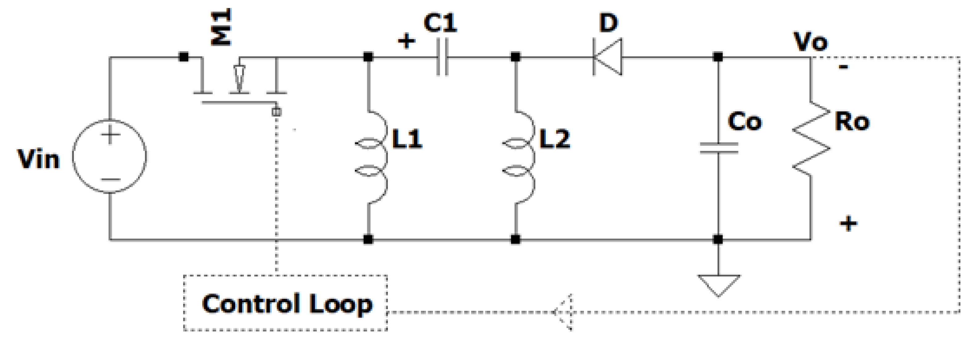
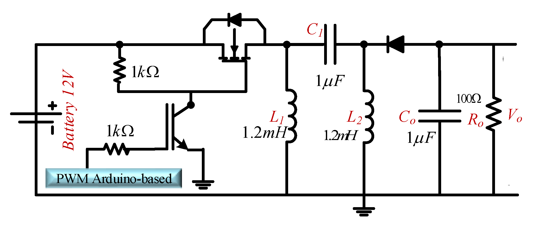
2.1. Operating Mode of the Proposed Converter

The proposed converter has two different operating modes as follows:
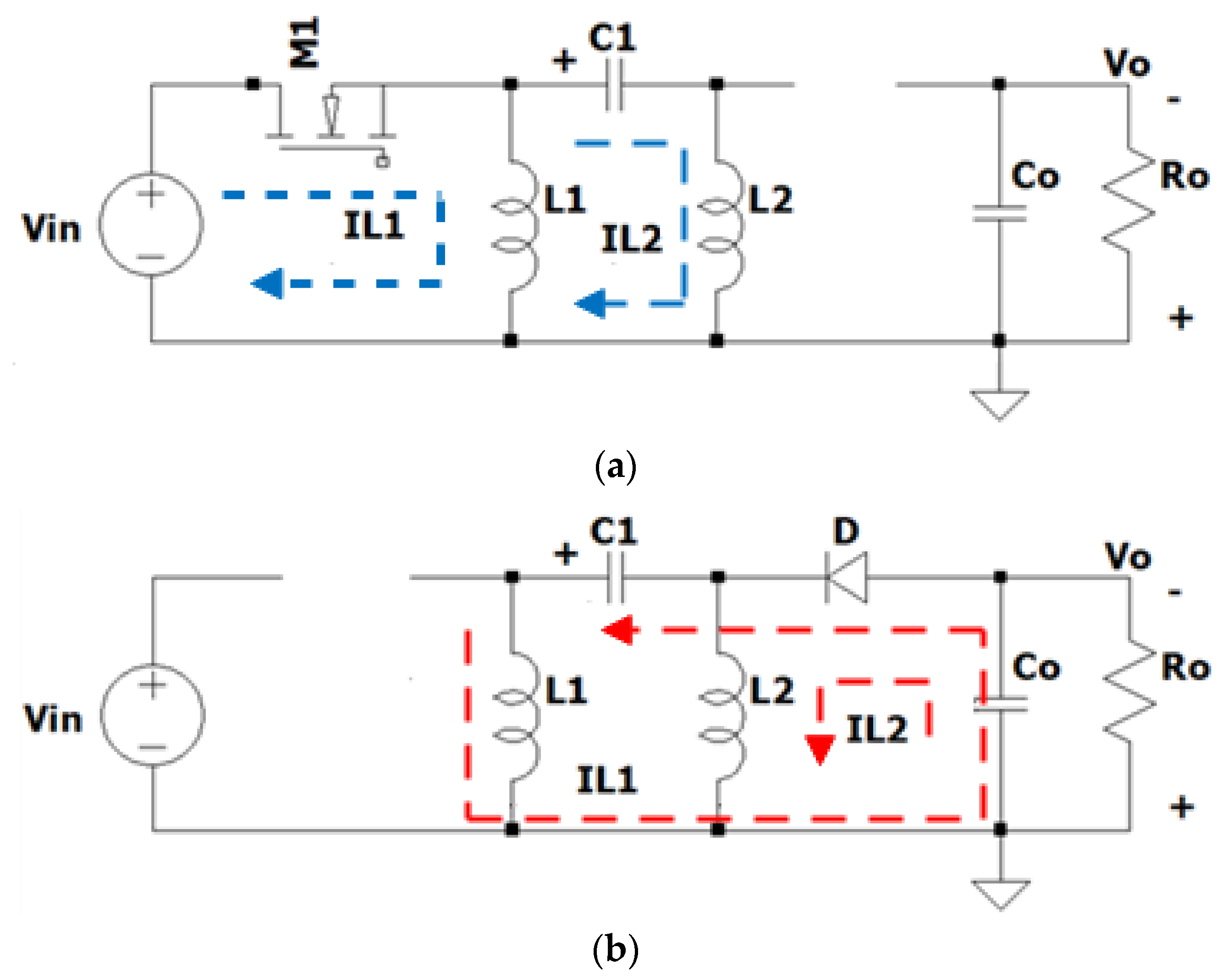
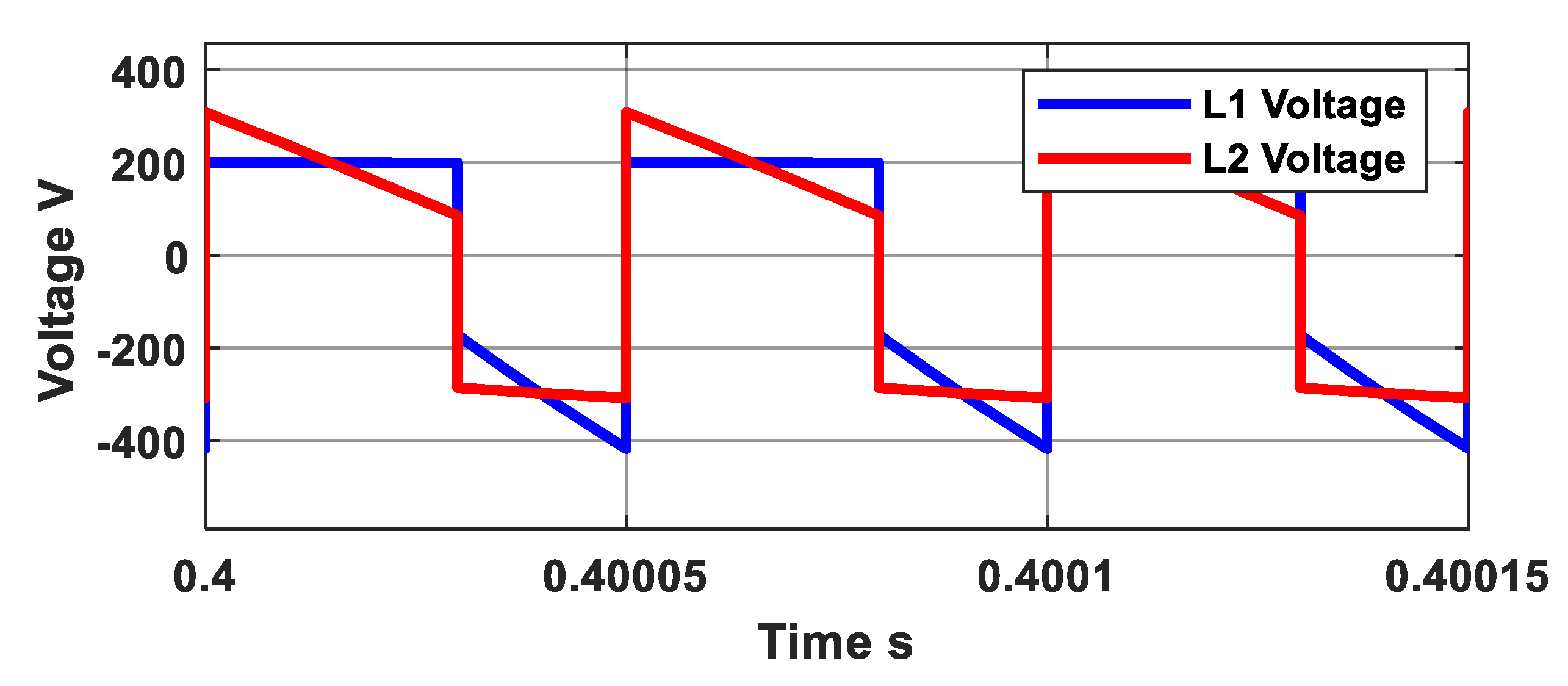
  • When the switch M1 is ON: the diode D is reversed biased. Figure 3a shows the equivalent circuit and current directions of this mode. The energy is transferred and stored in the coupling capacitor C1. Meanwhile, both inductors L1 and L2 are energized. The current slope in the inductors is given according to the following equations:
d I L 1 d t = V i n L 1
  d I L 2 d t = V i n + V C 1 L 2
Figure 3. (a) Mode 1, when switch M1 is on, (b) Mode 2, when switch M2 is off.
Sustainability 15 08515 g003
From (1) and (2), the switch current is the sum of two inductors’ current. This can be written as (3). Instantaneously, the voltage of capacitor C1 is given by (4).
I M 1 = I L 1 + I L 2
  V C 1 = V i n V L 2
  • When the switch M1 is OFF: the diode is forward and conducts the current. Figure 3b shows this mode’s equivalent circuit and current directions. All the energy stored in C1, L1, and L2 is transferred to the load. The current slope in the inductors is given according to the following equations:
d I L 1 d t = V o + V C 1 L 1
  d I L 2 d t = V i n + V C 1 L 2
From (5) and (6), the diode current is the sum of two inductors’ current. This can be written as on (7). Instantaneously, the voltage of capacitor C1 is given by (8).
I D = I L 1 + I L 2
  V C 1 = V L 1 V o
In the steady state, the average inductors’ voltages are zero. Based on (4) and (8) and the capacitance C1 is large enough, then, the average C1 voltage has to be equal to the following equation:
V C 1 = V L 1 V L 2
According to (9), it can be seen that the capacitor voltage C1 depends on the voltage difference between the two inductors. In the proposed converter, the coupling capacitor’s average voltage is equal to zero. This means all the energy stored during the turn-on period is dissipated during the turn-off period. More details will be discussed in the Simulation Results Section.

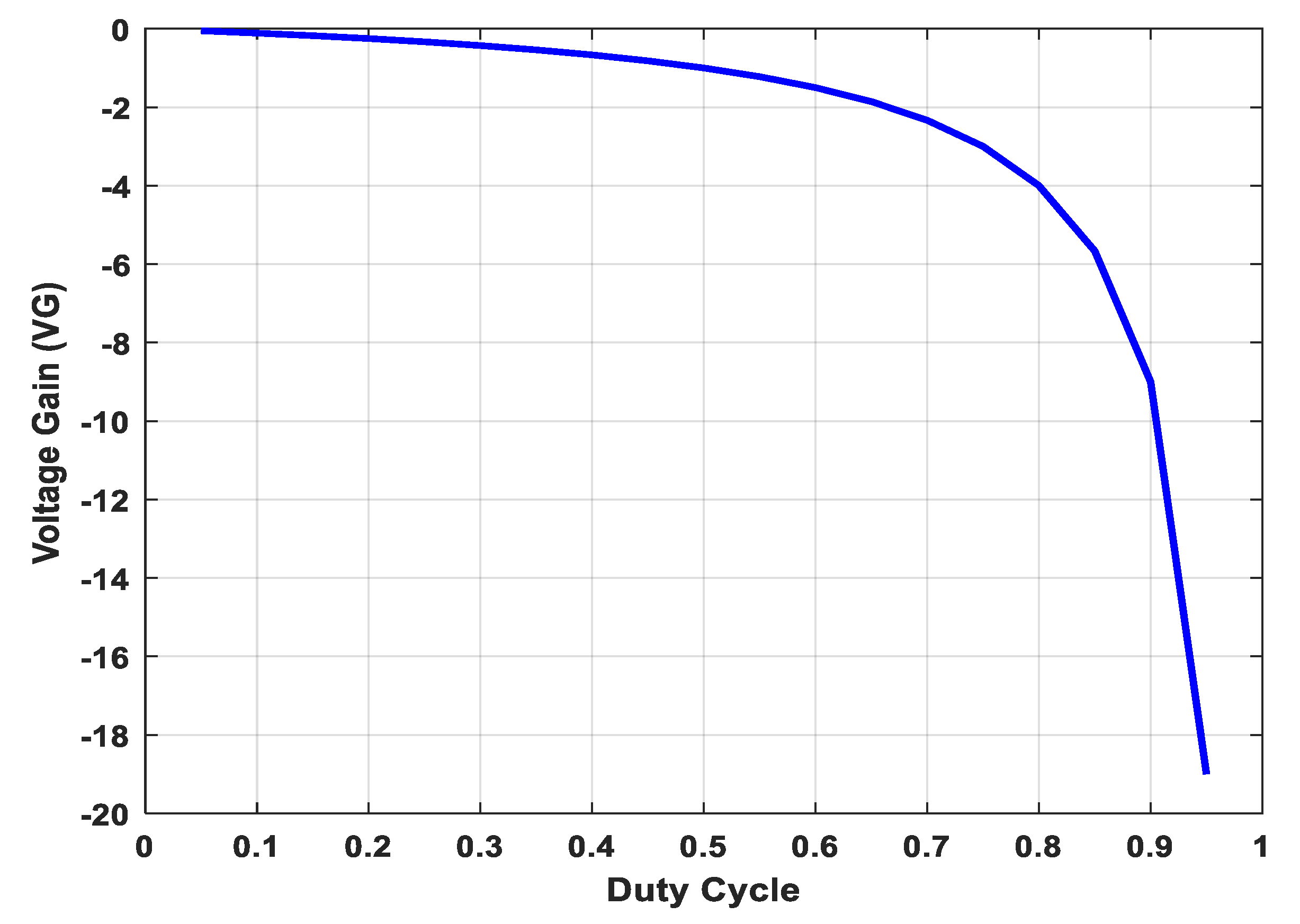
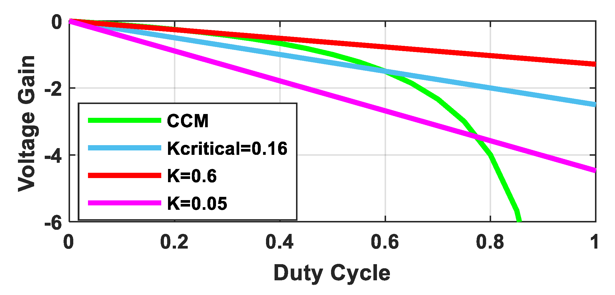
2.2. Duty Cycle and Voltage Gain of the Proposed Converter

The duty cycle of the proposed converter can be calculated based on the same procedure used in other DC-DC converters. In a steady state, the average inductor voltages over one switching cycle (Ts) must equal zero. Then, once the switch M1 is turned on, the inductor L1 is energized from the input DC voltage Vin. On the other hand, when the switch M1 is turned off, the energy stored in L1 is delivered to the load through the coupling capacitor C1 and the diode D. Based on that, the inductor voltage function is given by:
  V L 1 ( t ) = V i n , 0 < t < D T s V o     D T s < t < T s  
  V L 2 ( t ) = V i n , 0 < t < D T s V o ,   D T s < t < T s  
Calculating the average voltages of L1 and L2 results in (12). By solving (12), the voltage gain can be produced as per (13).
V L 1 = D T s V i n + ( 1 D ) T s V o = 0
  V G = V o V i n = D 1 D
where VG is the voltage gain of the proposed converter.
Equation (12) shows that the voltage gain of the proposed converter is the same as Buck–Boost, Cuk, and SEPIC converters [32]. Nevertheless, the proposed converter has an inverted output voltage, which can be used to step up and down by selecting a proper duty cycle value (see (13)). Additionally, it can be seen that the critical value between the step-up and step-down is D = 50%. Figure 4 plots the voltage gain of the proposed converter and the converter duty cycle.

3. Design Example and Parameters Selection

As seen in Figure 2, the proposed converter comprises a single controlled switch, a single diode, two decoupled inductors, one coupling capacitor, and one low-pass filter (shunt filter capacitor with load resistance). For simplicity, the proposed converter is assumed to work in continuous current mode (CCM). The following discussion confirms a proper selection of the converter parameters to achieve CCM operating mode.
The selected design parameters are based on the data presented in [33]; the DC output voltage (motor voltage) is 48 V. Nevertheless, in this paper, it is changed to 300 V for better indication, and the rated power of the motor is 1 kW. As the input voltage to the circuit in [28] is an AC RMS line voltage, then the average of the rectified voltage is calculated to equal 200 V-DC. In addition, the switching frequency is set to 20 kHz. The ripple current percentage in both inductor currents is set to 20%. In contrast, the ripple in the output voltage should not exceed 10% of the desired output voltage. Table 2 presents the selected parameters for the design along with their corresponding values. These parameters were derived from the application proposed in [33]. The calculated parameters based on the presented equations are included in the fourth and fifth columns.
The average inductor L1, L2 currents are calculated as:
  I L 1 = P o V i n
  I L 2 = P o V o
The load resistance is set according to (16), and then the selected inductors are given by (17) and (18), (when D = 0.6).
  R o = V o 2 P o
  I L 1 , max = V i n D f s Δ I L 1
  I L 2 , max = V o ( 1 D ) f s Δ I L 2
When selecting the coupling capacitor C1, the ripple in the output voltage should not exceed 20% of Vo, thus it is found as per (19). Finally, the filter capacitor can be calculated by using (20). Thus, Co has a minimum value calculated as:
  C 1 = V C 1 D R o f s Δ V C 1
C o = V o D R o f s Δ V C o  

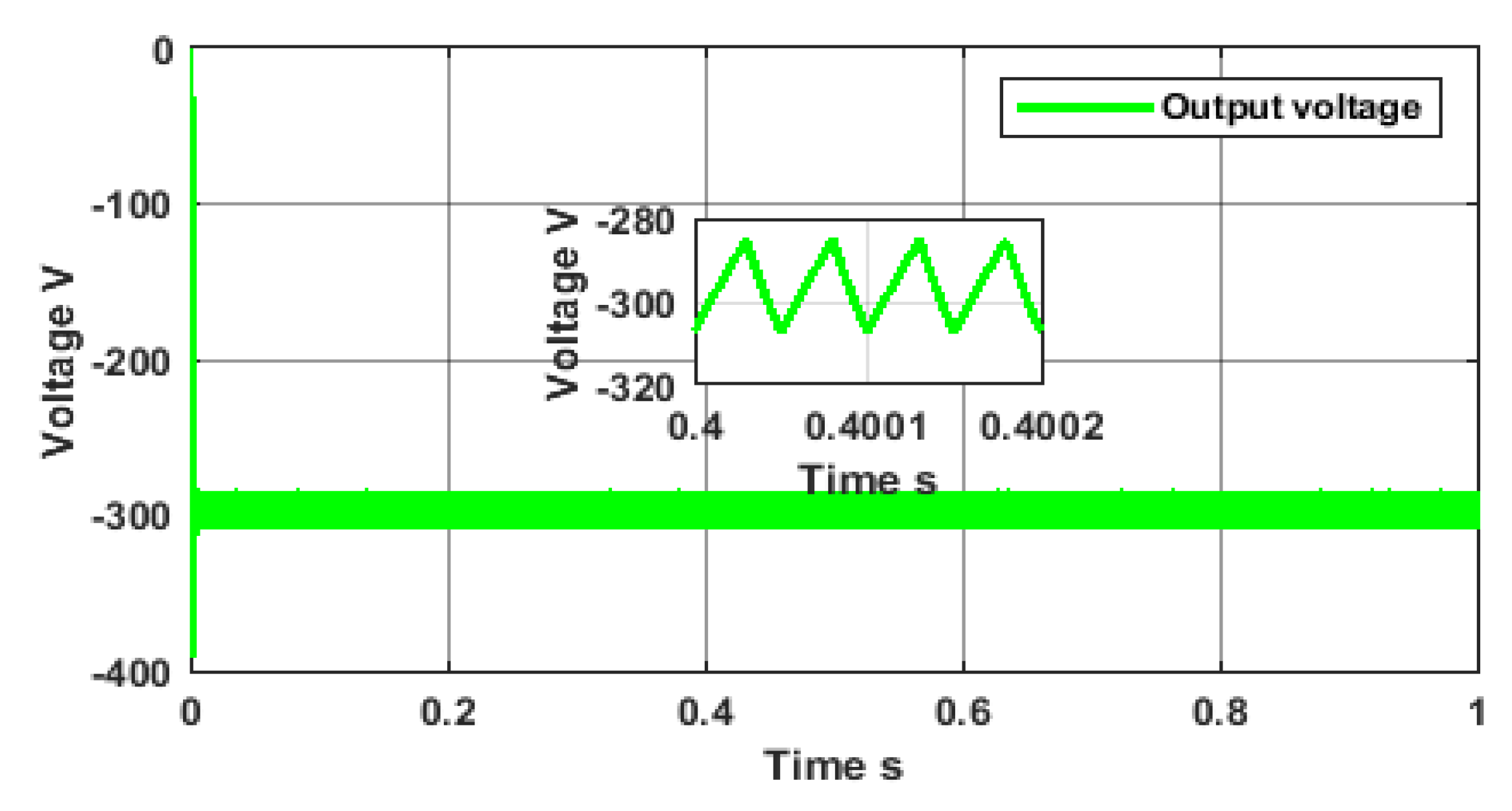
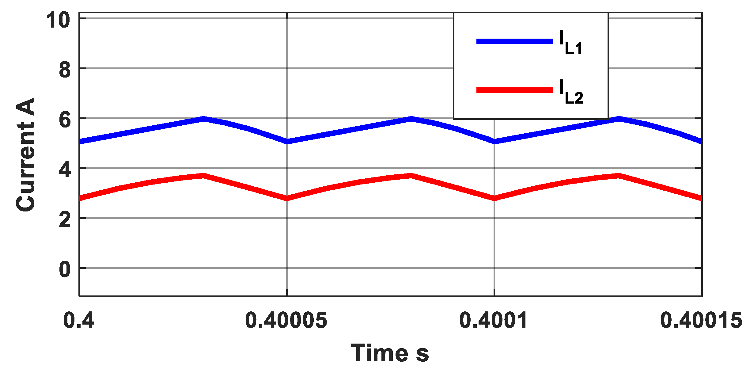
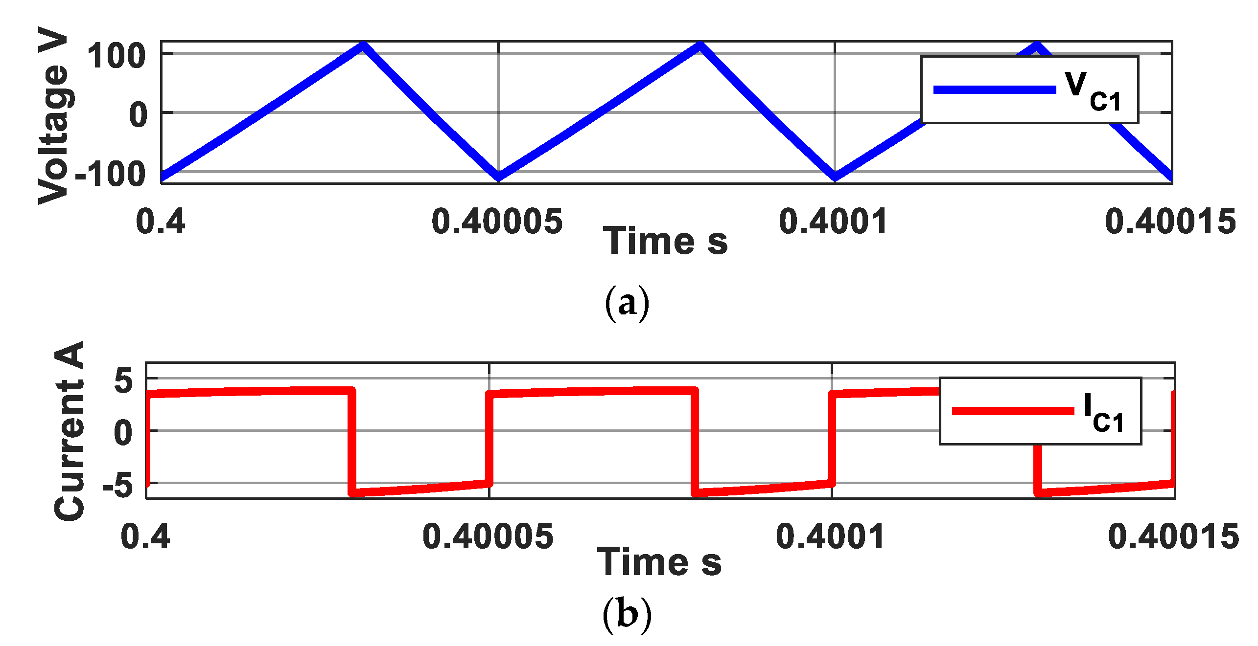
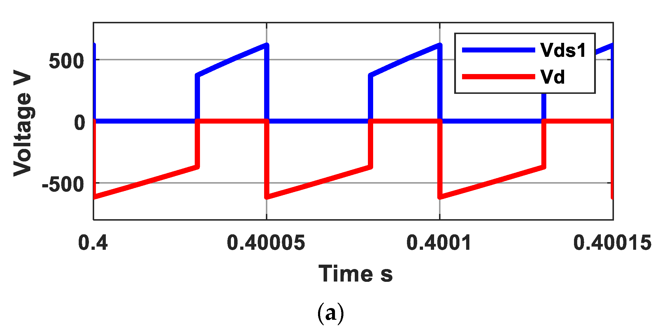
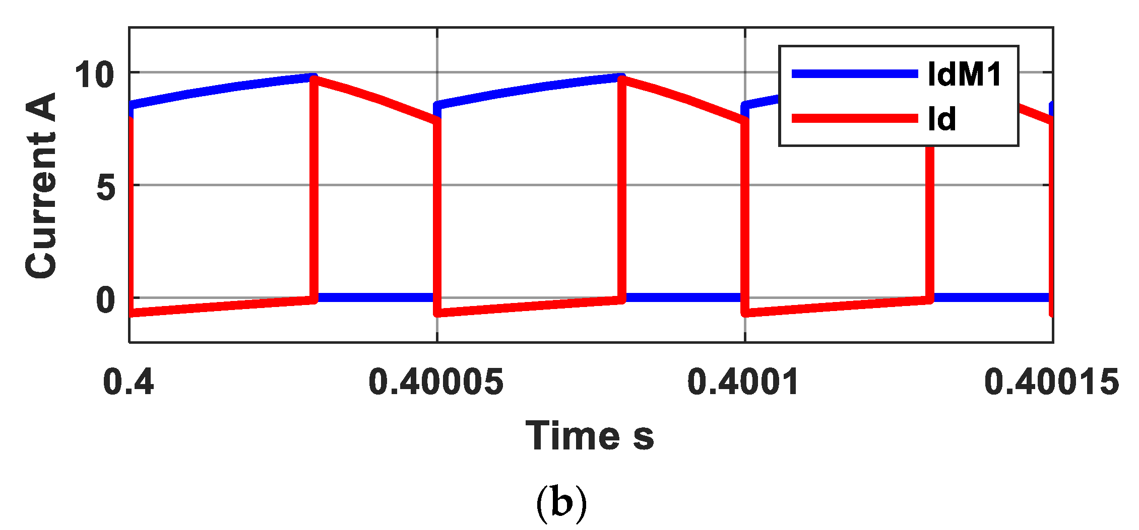
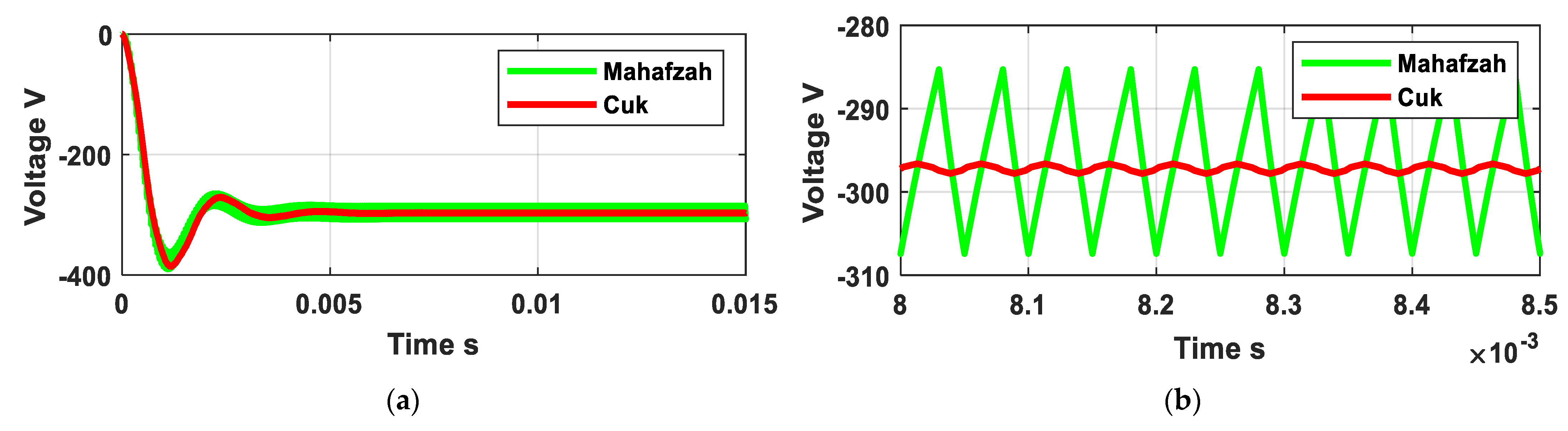
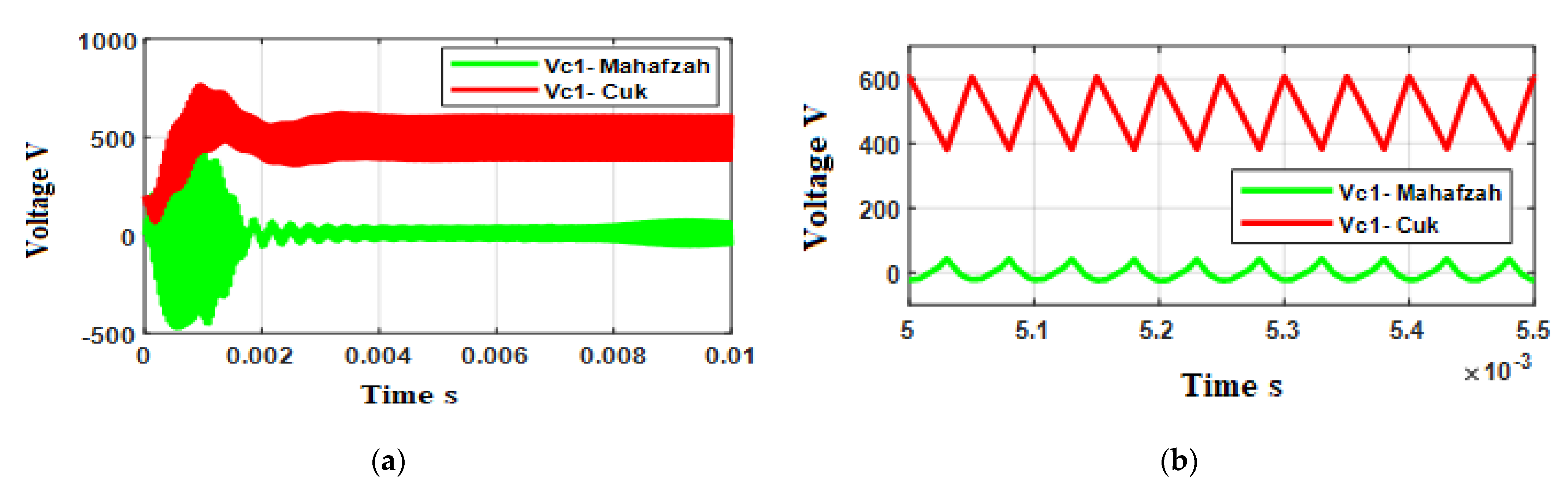
4. Simulation Results

MATLAB 2020a is used to simulate the proposed converter, which can provide very close results to the real prototype. The simulation parameters are discussed in the previous section, whereas the simulation time is set to 1 s, and the solver is selected to be an ordinary differential equation ode23tb with a maximum step size is 250 µs and continuous simulation type. Moreover, the proposed converter is operating under the CCM mode with a hard-switching technique and constant duty cycle equal to 0.6.
The output voltage is plotted in Figure 5. It is seen that the average output is 297 V DC voltage with a ripple percentage in the voltage of around 6.7%, which is an acceptable value. Moreover, as the load is a pure resistance, the load current has the same voltage pattern but is scaled by (1/90), which gives the average load current 3.3 A. Thus, the current ripple in IL1 is given by (21). Based on the design example (21) gives 0.92 A. Otherwise, the ripple in IL2 is calculated based on (22). It is also important to point out that the result of (21) is 1.3 A.
  Δ I L 1 = V i n D T s L 1  
  Δ I L 2 = V o D T s L 2  
The continuous current operation in the proposed converter is clearly seen in Figure 6. As the inductance values of both inductors are the same, the difference in the slopes and their averages are related to the difference in the applied voltage across inductor terminals during the on/off periods. The average inductor current IL1 is equal to 5 A, and the average inductor current IL2 is equal to 3.3 A, with a ripple current percentage of less than 20% of both currents.
On the other hand, the inductors’ voltages are illustrated in Figure 7. During the conduction of switch M1, the L1 is clamped to Vin. Meanwhile, the L2 voltage to the difference between VL1 and VC1. During the conduction period of the diode, the L1 has a voltage of VL2 + VC1 but in the reverse direction, and the L2 voltage is clamped to the load voltage. In steady-state operation, the average inductor voltages are equal to zero. Figure 8 presents the coupling capacitor voltage and its current. Over one switching cycle, it is noticeable that the capacitor bypasses the energy from the input side to the output side without any remaining voltage across its terminals. This means the average capacitor voltage is zero based on Figure 8a. Additionally, the balance in the capacitor charge is illustrated in Figure 8b. Whereas, the average capacitor current over one switching cycle is zero in steady-state conditions.
The merit of the proposed converter is the existence of an LCL tank connected with the switch M1, this connection offers a soft switching turn on and turn off. The voltage stress across the switch is illustrated in Figure 9a. The voltage reaches the sum of Vin + VC1 + Vo. The same issue with the output diode. Figure 9b shows the switch and diode currents. The average switch and diode voltages are calculated, respectively, using the following equations:
  I M 1 = V i n D 2 R o ( 1 D ) 2  
  I D = V i n D R o ( 1 D )  
The proposed converter is compared with the Cuk converter. The Cuk converter is simulated using the same design example discussed above to compare the results. Both converters’ output voltages are shown in Figure 10a. It shows that the output voltage in both cases decreased to −300 V, but the proposed converter has more ripple in its voltage than the Cuk converter. Moreover, the proposed converter has an unrecognizable overshoot higher than the Cuk converter, but the proposed converter is faster than the Cuk converter in achieving the steady state period, see Figure 10b.
The coupling capacitor C1 plays an important role in energy transfer in Cuk, SEPIC, Buck–Boost, and Luo converters, as well as it has a role in the proposed Mahafzah converter. The selected capacitor must be sized so that it has a rated voltage value that is higher than twice the voltage across its terminal. The higher rated voltage results in a higher size capacitor. Furthermore, the large size of this capacitor holds a rather large place on the PCB, thus reducing the cost of circuit manufacturing.
Figure 11a compares the two capacitor voltages in the proposed and Cuk converter. As noticed from Figure 11b, the coupling capacitor Cuk converter has a much higher applied voltage than its counterpart in the proposed converter. Similar to the Cuk converter, the proposed converter has the boundary characteristics shown in Figure 12. The coupling capacitor is selected to endure the applied voltage across its terminal in the Cuk converter. The critical value that separates the two modes is plotted in the cyan curve. The voltage gain as a function of the duty cycle and K value is given by (25). Then, according to (25), the critical value between CCM and DCM is given as described in (26). Accordingly, Kcritical is equal to 0.16.
  V G ( D , K ) = D 1 D K > K c r i t i c a l   D K     K > K c r i t i c a l
  K c r i t i c a l = ( 1 D ) 2
As illustrated in Figure 11 and in Equation (19), the coupling capacitor value of the proposed converter is noticeably reduced by five times compared to the coupling capacitor value for the cuck converter under the same operating conditions. The loss components of the proposed converter can be divided into conduction losses, switching losses, and control losses [23,34]. It should be noted that these losses are associated with semiconductor devices. Table 3 illustrates all loss components and provides the related equation.
Using the presented equations in Table 2, the efficiency of the proposed converter is calculated when changing the load simultaneously. The efficiency of the proposed converter is compared with the Cuk converter, as illustrated in Figure 13. The efficiency of both converters is calculated based on the equations presented in [22,23,24,34]. The efficiency calculation considers all the loss components, including the conduction, switching, and control losses. The efficiency is also calculated when the load current is changed from 10% up to 100% of the rated current. As seen in Figure 13, the proposed converter has better efficiency than the Cuk converter when the load is increased. The efficiency of the proposed converter reaches around 88% at full load conditions, while the Cuk converter efficiency reaches 87% at the same rated conditions.

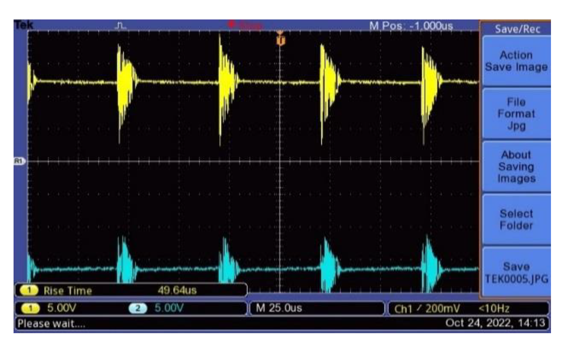
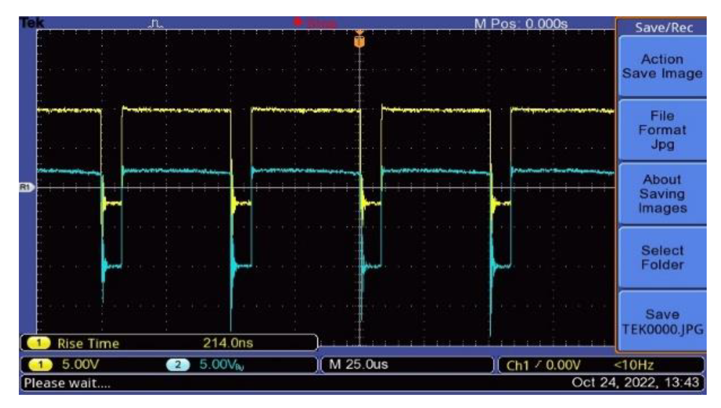
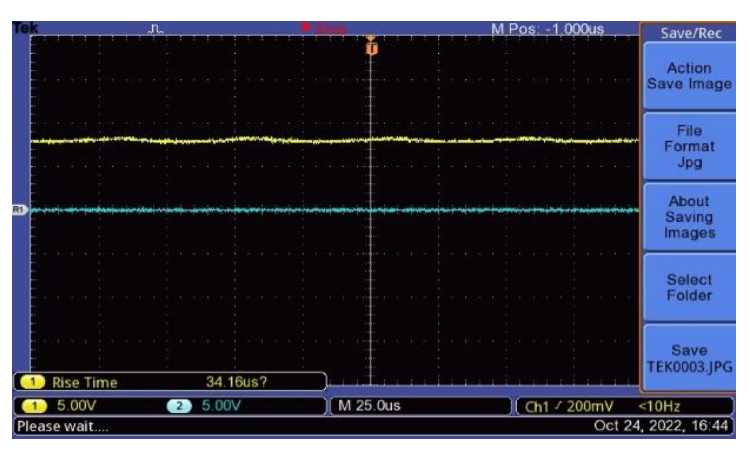
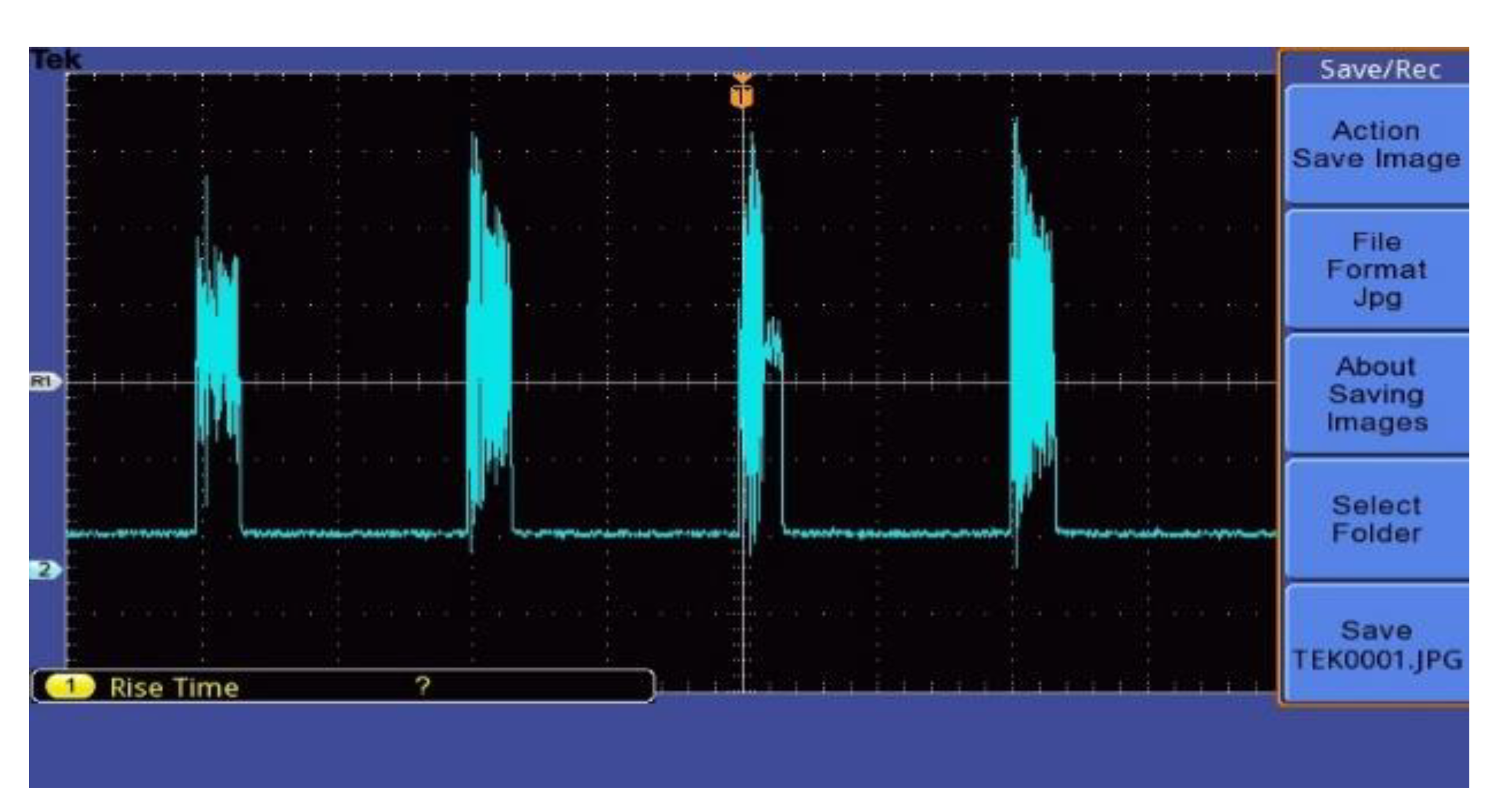
5. Experimental Results

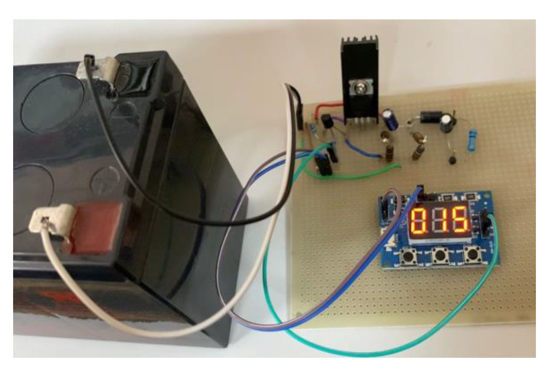
5.1. Experiment Setup

The experimental setup for testing the proposed configuration is illustrated in the circuit diagram (Figure 14). To validate the proposed converter, a low voltage–low power prototype (Figure 15) was constructed using the available equipment in the laboratory. The input voltage was set to 12 V by a standalone battery, and low-power inductors with an approximate value of 1.2 mH were selected. The load resistance was set to 100 Ω, resulting in an output voltage of −18 V and a converter power of 3.24 W. The available IRF540N MOSFET was utilized as the switch, controlled by an N-type transistor 2N3904 through an Arduino-based chip, allowing for adjustment of the duty cycle and switching frequency. Prior to conducting the measurements, the proposed converter was re-simulated using MATLAB/ Simulink with the parameters provided in Table 4.

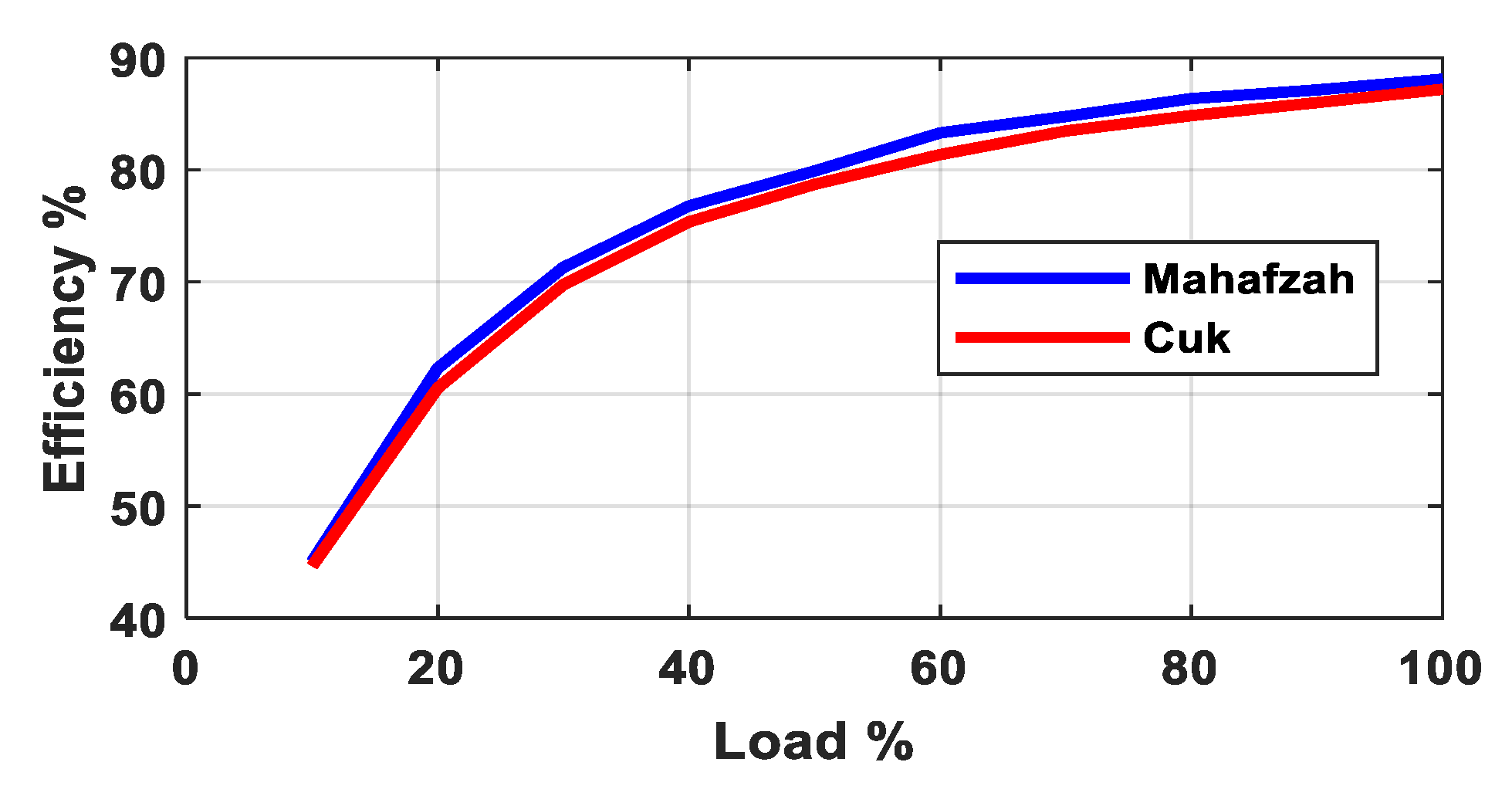
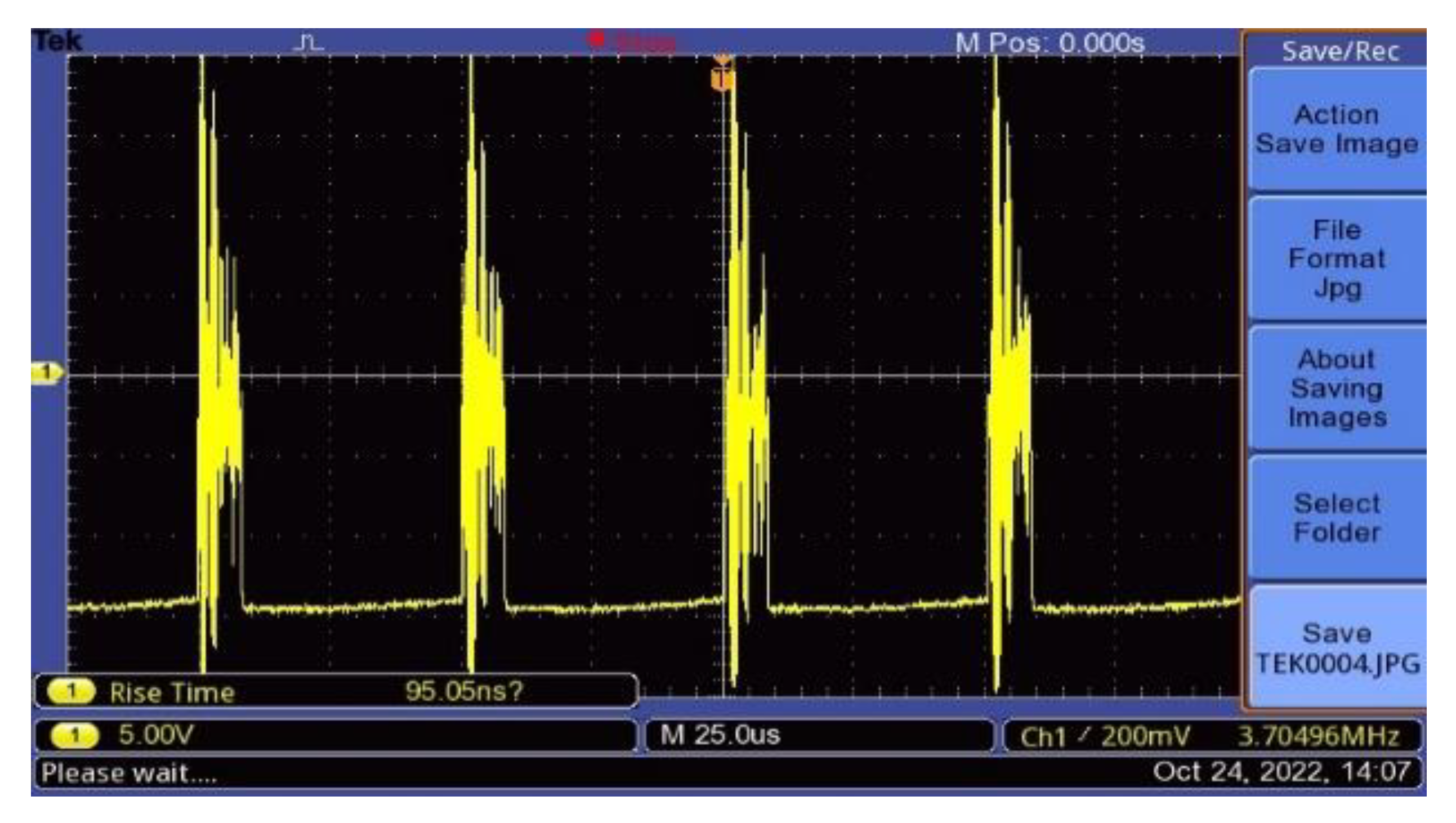
5.2. Experimental Results and Discussion

The output voltage is shown in Figure 16 (Ch2). The load voltage is recorded at −18 V with a low voltage ripple. The driving voltage of IRF540N is shown in Figure 16 (Ch1). The applied voltage reaches a peak of 12 V, with a duty cycle is about 70% (35 µs). Accordingly, the inductor L1 voltage is plotted in Figure 17.
As observed in Figure 17 (Ch1), the inductor voltage reaches 12 V (the input voltage) during the switch M1’s turn-on time. However, when the switch is turned off (with an off time of approximately 15 µs), the inductor voltage decreases to −6 V. Similarly, during the switch M1’s turn-on time, the inductor L2 exhibits a voltage of a 3 V across its terminals. Conversely, when the switch M1 is turned off, the inductor L2 displays −10 V, see Figure 17 (Ch2). In addition, the coupling capacitor has 7 V across its terminal, which corresponds to the difference between the input and output voltage. Consequently, the rated voltage of the selected voltage of C1 should be around 15 V. This confirms that the selected coupling capacitor has a lower rated voltage than the same one in the Cuk converter (in the Cuk converter case, the rating voltage of the coupling capacitor must be selected around 45 V. This reduces the selected rated voltage of C1 in the proposed converter by 66.67% compared to the same capacitor of Cuk converter, as seen in Figure 18.
The drain-source voltage of the IRF540N is depicted in Figure 19, while the diode voltage is plotted in Figure 20. The MOSFET is operated with a duty cycle of 70%. It can be seen from these Figures that during the switch turn-off period, there is some ringing present in the voltage waveform. This ringing is related to some reasons, such as: one reason is the resonance between L1 and the MOSFET’s parasitic capacitance during the energy transfer period. It is not possible to resonate L2 and C1 with L1, because the resonant frequency of this combination is about 28 kHz. Similarly, there is no possible resonant between L2 and C1 with L1, as their resonance frequency is about 40 kHz, significantly lower than the frequency depicted in Figure 19 and Figure 20.
The second reason is the possible resonance between the inductance of L1 and the capacitance of parasitic capacitance of the used passive prob. The third possible reason may be related to the poor copper board used which causes some EMI issues. However, these reasons can be easily overcome with very good PCB design and using advanced measuring devices. In sum, Table 5 provides a comprehensive comparison between the Cuk converter and the Mahafzah converter, considering their main features under the same operating conditions.
Overall, based on the information provided in the table, the Mahafzah converter demonstrates certain advantages over the Cuk converter in terms of the reduced coupling capacitor voltage, improved efficiency, and shorter transient period. However, it is important to note that the table does not provide specific quantitative values or detailed explanations for each feature, making it difficult to conduct a thorough analysis without further information.

6. Conclusions

This paper proposed a DC-DC converter based on the Cuk converter, namely the Mahafzah converter. The proposed converter maintains the same component counts, duty cycle, voltage gain, and inverted output voltage as the Cuk converter, but with a different arrangement and new design. The new configuration of the proposed converter offers the advantage of reducing the rating voltage of the coupling capacitor, resulting in a smaller size and lower cost. Additionally, it operates at a lower rated voltage of the coupling capacitor. Moreover, the currents of the semiconductor devices are reduced compared to those in the devices in the Cuk converter. As a result, the losses in the proposed converter are reduced, leading to improved efficiency. The operating modes and mathematical equations governing the currents and voltages of the inductors, coupling capacitor, switch, and diode are thoroughly discussed in this paper. A design example is presented to verify the effectiveness of the proposed configuration. The design is validated through simulation to evaluate the operation, performance, and efficiency of the converter. Experimental tests are also conducted to validate the simulation results. For this purpose, a low voltage–low power prototype (12/−18 V, 3.24 W) is built to verify the operation and validate the proposed converter waveforms. The results demonstrate the excellent performance of the new converter, as evidenced by the matching between the simulation and design calculation results. Furthermore, the proposed converter exhibits higher efficiency than the Cuk converter under load variations, with an efficiency of 88% at rated load conditions, surpassing the Cuk converter by 1%. All the highlighted insights of this new design will hopefully lead to increased efforts toward the development of advanced energy conversion for electric vehicles and hybrid renewable energy systems.

Author Contributions

Conceptualization, K.A.M.; methodology, K.A.M. and A.Q.A.-S.; software, K.A.M. and N.N.; validation, M.A.H. and A.Q.A.-S.; formal analysis, K.A.M., A.Q.A.-S., T.S.B. and N.N.; experiment, K.A.M. and A.Q.A.-S.; investigation, K.A.M. and A.Q.A.-S.; writing—original draft preparation, K.A.M. and A.Q.A.-S.; writing—review and editing, K.A.M., T.S.B., N.N., A.Q.A.-S. and M.A.H.; project administration, M.A.H. All authors have read and agreed to the published version of the manuscript.

Funding

This research received no external funding.

Institutional Review Board Statement

Not applicable.

Informed Consent Statement

Not applicable.

Data Availability Statement

Not applicable.

Conflicts of Interest

The authors declare no conflict of interest.

References

  1. Cao, L.; Loo, K.H.; Lai, Y.M. Output-Impedance Shaping of Bidirectional DAB DC–DC Converter Using Double-Proportional-Integral Feedback for Near-Ripple-Free DC Bus Voltage Regulation in Renewable Energy Systems. IEEE Trans. Power Electron. 2016, 31, 2187–2199. [Google Scholar] [CrossRef]
  2. Zeng, J.; Du, X.; Yang, Z. A Multiport Bidirectional DC–DC Converter for Hybrid Renewable Energy System Integration. IEEE Trans. Power Electron. 2021, 36, 12281–12291. [Google Scholar] [CrossRef]
  3. He, P.; Khaligh, A. Comprehensive Analyses and Comparison of 1 kW Isolated DC–DC Converters for Bidirectional EV Charging Systems. IEEE Trans. Transp. Electrif. 2017, 3, 147–156. [Google Scholar] [CrossRef]
  4. Heydari-Doostabad, H.; O’Donnell, T. A Wide-Range High-Voltage-Gain Bidirectional DC–DC Converter for V2G and G2V Hybrid EV Charger. IEEE Trans. Ind. Electron. 2022, 69, 4718–4729. [Google Scholar] [CrossRef]
  5. Prabhakaran, P.; Agarwal, V. Novel Boost-SEPIC Type Interleaved DC–DC Converter for Mitigation of Voltage Imbalance in a Low-Voltage Bipolar DC Microgrid. IEEE Trans. Ind. Electron. 2020, 67, 6494–6504. [Google Scholar] [CrossRef]
  6. Gui, Y.; Han, R.; Guerrero, J.M.; Vasquez, J.C.; Wei, B.; Kim, W. Large-Signal Stability Improvement of DC–DC Converters in DC Microgrid. IEEE Trans. Energy Convers. 2021, 36, 2534–2544. [Google Scholar] [CrossRef]
  7. Hazucha, P.; Moon, T.S.; Schrom, G.; Paillet, F.; Gardner, D.; Rajapandian, S.; Karnik, T. High Voltage Tolerant Linear Regulator with Fast Digital Control for Biasing of Integrated DC–DC Converters. IEEE J. Solid-State Circuits 2007, 42, 66–73. [Google Scholar] [CrossRef]
  8. Subasinghage, K.; Gunawardane, K.; Kularatna, N.; Lie, T.T. Extending the Supercapacitor-Assisted Low-Dropout Regulator (SCALDO) Technique to a Split-Rail DC–DC Converter Application. IEEE Access 2019, 7, 124034–124047. [Google Scholar] [CrossRef]
  9. Liu, M.; Zhang, D.; Zhou, Z. Linear Regulator Design Considerations of the Serial Linear-Assisted Switching Converter Used as Envelope Amplifier. IEEE Trans. Power Electron. 2016, 31, 3673–3689. [Google Scholar] [CrossRef]
  10. Czarkowski, D.; Kazimierczuk, M.K. Linear circuit models of PWM flyback and buck/boost converters. IEEE Trans. Circuits Syst. I Fundam. Theory Appl. 1992, 39, 688–693. [Google Scholar] [CrossRef]
  11. Bhatia, D.; Xue, L.; Li, P.; Wu, Q.; Bashirullah, R. High-voltage tolerant digitally aided DCM/PWM multiphase DC-DC boost converter with integrated Schottky diodes in 0.13 µm 1.2 V digital CMOS process. IEEE J. Solid-State Circuits 2013, 48, 774–789. [Google Scholar] [CrossRef]
  12. Do, H. Zero-Voltage-Switching Synchronous Buck Converter with a Coupled Inductor. IEEE Trans. Ind. Electron. 2011, 58, 3440–3447. [Google Scholar] [CrossRef]
  13. Azer, P.; Emadi, A. Generalized State Space Average Model for Multi-Phase Interleaved Buck, Boost and Buck-Boost DC–DC Converters: Transient, Steady-State and Switching Dynamics. IEEE Access 2020, 8, 77735–77745. [Google Scholar] [CrossRef]
  14. Memon, A.H.; Baloach, M.H.; Sahito, A.A.; Soomro, A.M.; Memon, Z.A. Achieving High Input PF for CRM Buck-Buck/Boost PFC Converter. IEEE Access 2018, 6, 79082–79093. [Google Scholar] [CrossRef]
  15. Siwakoti, Y.P.; Mostaan, A.; Abdelhakim, A.; Davari, P.; Soltani, M.N.; Khan, N.H.; Li, L.; Blaabjerg, F. High-Voltage Gain Quasi-SEPIC DC–DC Converter. IEEE J. Emerg. Sel. Top. Power Electron. 2019, 7, 1243–1257. [Google Scholar] [CrossRef]
  16. Anand, A.; Singh, B. Modified Dual Output Cuk Converter-Fed Switched Reluctance Motor Drive with Power Factor Correction. IEEE Trans. Power Electron. 2019, 34, 624–635. [Google Scholar] [CrossRef]
  17. Singh, B.; Kushwaha, R. Power Factor Preregulation in Interleaved Luo Converter-Fed Electric Vehicle Battery Charger. IEEE Trans. Ind. Appl. 2021, 57, 2870–2882. [Google Scholar] [CrossRef]
  18. Sarani, S.; Zarchi, H.A.; Delavaripour, H. Ripple-Free Input Current Flyback Converter Using a Simple Passive Circuit. IEEE Trans. Ind. Electron. 2022, 69, 2557–2564. [Google Scholar] [CrossRef]
  19. Li, G.; Xia, J.; Wang, K.; Deng, Y.; He, X.; Wang, Y. Hybrid Modulation of Parallel-Series LLC Resonant Converter and Phase Shift Full-Bridge Converter for a Dual-Output DC–DC Converter. IEEE J. Emerg. Sel. Top. Power Electron. 2019, 7, 833–842. [Google Scholar] [CrossRef]
  20. Ma, X.; Wang, P.; Bi, H.; Wang, Z. A Bidirectional LLCL Resonant DC–DC Converter with Reduced Resonant Tank Currents and Reduced Voltage Stress of the Resonant Capacitor. IEEE Access 2020, 8, 125549–125564. [Google Scholar] [CrossRef]
  21. Wang, C. A Novel ZCS-PWM Flyback Converter With a Simple ZCS-PWM Commutation Cell. IEEE Trans. Ind. Electron. 2008, 55, 749–757. [Google Scholar] [CrossRef]
  22. Zhang, F.; Yan, Y. Novel Forward–Flyback Hybrid Bidirectional DC–DC Converter. IEEE Trans. Ind. Electron. 2009, 56, 1578–1584. [Google Scholar] [CrossRef]
  23. Mahafzah, K.A.; Krischan, K.; Muetze, A. Efficiency enhancement of a three phase Hard Switching Inverter under light load conditions. In Proceedings of the IECON 2016—42nd Annual Conference of the IEEE Industrial Electronics Society, Florence, Italy, 23–26 October 2016; pp. 3372–3377. [Google Scholar] [CrossRef]
  24. Shen, Y.; Wang, H.; Al-Durra, A.; Qin, Z.; Blaabjerg, F. A Structure-Reconfigurable Series Resonant DC–DC Converter with Wide-Input and Configurable-Output Voltages. IEEE Trans. Ind. Appl. 2019, 55, 1752–1764. [Google Scholar] [CrossRef]
  25. Mahafzah, K.A.; Obeidat, M.A.; Al-Shetwi, A.Q.; Ustun, T.S. A Novel Synchronized Multiple Output DC-DC Converter Based on Hybrid Flyback-Cuk Topologies. Batteries 2022, 8, 93. [Google Scholar] [CrossRef]
  26. Basić, M.; Dujić, D. Hybrid modular multilevel converter for variable DC link voltage operation. CPSS Trans. Power Electron. Appl. 2021, 6, 178–190. [Google Scholar] [CrossRef]
  27. Safayatullah, M.; Elrais, M.T.; Ghosh, S.; Rezaii, R.; Batarseh, I. A Comprehensive Review of Power Converter Topologies and Control Methods for Electric Vehicle Fast Charging Applications. IEEE Access 2022, 10, 40753–40793. [Google Scholar] [CrossRef]
  28. Alatai, S.; Salem, M.; Ishak, D.; Das, H.S.; Alhuyi Nazari, M.; Bughneda, A.; Kamarol, M. A Review on State-of-the-Art Power Converters: Bidirectional, Resonant, Multilevel Converters and Their Derivatives. Appl. Sci. 2021, 11, 10172. [Google Scholar] [CrossRef]
  29. Richelli, A.; Salem, M.; Colalongo, L. A Review of Fully Integrated and Embedded Power Converters for IoT. Energies 2021, 14, 5419. [Google Scholar] [CrossRef]
  30. Zhang, N.; Sutanto, D.; Muttaqi, K.M. A review of topologies of three-port DC–DC converters for the integration of renewable energy and energy storage system. Renew. Sustain. Energy Rev. 2016, 56, 388–401. [Google Scholar] [CrossRef]
  31. Salem, M.; Jusoh, A.; Idris, N.R.N.; Das, H.S.; Alhamrouni, I. Resonant power converters with respect to passive storage (LC) elements and control techniques–An overview. Renew. Sustain. Energy Rev. 2018, 91, 504–520. [Google Scholar] [CrossRef]
  32. Pop-Calimanu, I.M.; Popescu, S.; Lascu, D. A New SEPIC-Based DC–DC Converter with Coupled Inductors Suitable for High Step-Up Applications. Appl. Sci. 2021, 12, 178. [Google Scholar] [CrossRef]
  33. Kushwaha, R.; Singh, B. A Modified Bridgeless Cuk Converter based EV Charger with Improved Power Quality. In Proceedings of the 2019 IEEE Transportation Electrification Conference and Expo (ITEC), Detroit, MI, USA, 19–21 June 2019; pp. 1–6. [Google Scholar] [CrossRef]
  34. Mahafzah, K.A.; Krischan, K.; Muetze, A. Efficiency enhancement of a three phase Soft Switching Inverter under light load conditions. In Proceedings of the IECON 2016—42nd Annual Conference of the IEEE Industrial Electronics Society, Florence, Italy, 23–26 October 2016; pp. 3378–3383. [Google Scholar] [CrossRef]
Figure 2. The proposed Mahafzah converter.
Sustainability 15 08515 g002
Figure 4. The voltage gain change based on the converter duty cycle.
Sustainability 15 08515 g004
Figure 5. The output voltage of the proposed Mahafzah converter.
Sustainability 15 08515 g005
Figure 6. Inductor currents in CCM.
Sustainability 15 08515 g006
Figure 7. The inductors voltages in CCM.
Sustainability 15 08515 g007
Figure 8. (a) The voltage of coupling capacitor C1 (b). The current of coupling capacitor C1.
Sustainability 15 08515 g008
Figure 9. (a) The switch M1 voltage (blue), and the diode D (red) voltage (b). The switch M1 current (blue), and the diode D (red) current.
Sustainability 15 08515 g009aSustainability 15 08515 g009b
Figure 10. (a) The output voltage of both converters, (b) the zoomed in.
Sustainability 15 08515 g010
Figure 11. (a) The coupling capacitor voltage of both converters, (b) zoomed in during steady state.
Sustainability 15 08515 g011
Figure 12. Characteristics of the proposed converter.
Sustainability 15 08515 g012
Figure 13. The efficiency of both converters.
Sustainability 15 08515 g013
Figure 14. Circuit diagram of the experimental setup (new configuration proposed).
Sustainability 15 08515 g014
Figure 15. The 3.24 W/−18 V converter prototype.
Sustainability 15 08515 g015
Figure 16. Ch1: Input Voltage, Ch2: Output Voltages.
Sustainability 15 08515 g016
Figure 17. Ch1: VL1, Ch2: VL2.
Sustainability 15 08515 g017
Figure 18. C1 Voltage.
Sustainability 15 08515 g018
Figure 19. Drain-source voltage.
Sustainability 15 08515 g019
Figure 20. Diode voltage.
Sustainability 15 08515 g020
Table 1. Different DC-DC converters topologies with their limitations.
Ref.Year of PublicationObjectiveLimitations
[12]2011A buck converter with coupled inductor for ZVS is proposedCritical design of the coupled inductor
[13]2020A different DC-DC converters with average model is presentedIt is used for multi-phase applications with coupled inductor
[15]2018Design quasi-SEPIC converter with high voltage gain capabilityIt uses a coupled inductor and the way to improve the magnetic core characteristics
[16]2019Proposes a new Cuk converter fed switched reluctance motorThe circuit has additional semiconductor devices and many inductors
[17]2021Proposed an interleaved Luo converterThe critical design of the magnetic circuit
[18]2022Design a flyback with a ripple free in inductor current Adding many passive components to the conventional flyback
Table 2. The selected parameters of the design.
These Parameters Are Taken from the Application Proposed in [33]The Calculated Parameters Based on Presented Equations
ParameterValueParameterValue
Pin/Po1 kWIo3.3 A
Vin200 VIL15 A
Vo−300 VIL23.3 A
ΔIL10.92 ARo90 Ω
ΔIL21.3 AL16.5 mH
ΔVC1<0.1L26.5 mH
Kp0.2C10.5 µF
Ki0.001Co5 µF
Duty Cycle (D)60%
fs20 kHz
Table 3. Loss calculation of the proposed Mahafzah converter.
Loss ComponentEquationNote
Conduction Loss P M 1 = i d 2 R d s o n D Ron: MOSFET on-state resistance
P D = ( V f i d + i d 2 R f ) ( 1 D )
Switching Loss P M 1 = 05 f s C o s s ( 0.5 V i n + V o ) 2 C o s s is M1 output capacitance
P D = 05 f s C d ( 0.5 V i n + V o ) 2
Control Loss P g a t e s = Q g V g s f s Q g is the gate charge of M1
R L 1 = R 1 d c D T s V i n L 1 2
Passive Devices R L 2 = R 2 d c D T s V o L 2 2 Losses in each L1 and L2 based on using their DC resistance. The losses in the coupling capacitor are ignored due to its small ERS
Table 4. Selected parameters of the prototype.
The Selected Parameters for Testing and Validation
ParameterValue
Pin/Po3.24 W
Vin12 V
Vo−18 V
MOSFETIRF540N
Driving Transistor2N3904
Diode1N4007
L1 = L21.2 mH
C11 µF
Duty Cycle70%
fs20 kHz
Table 5. A comprehensive compression between Cuk and Mahafzah converters.
ParametersConverter Topology
Cuk ConverterMahafzah Converter
Component CountSameSame
Coupling Capacitor VoltageHighReduced (√)
EfficiencyLowImproved (√)
Ripple in VoLow (√)High
Transient PeriodLongShort (√)
“√” indicates which converter is better for each parameter.
Disclaimer/Publisher’s Note: The statements, opinions and data contained in all publications are solely those of the individual author(s) and contributor(s) and not of MDPI and/or the editor(s). MDPI and/or the editor(s) disclaim responsibility for any injury to people or property resulting from any ideas, methods, instructions or products referred to in the content.

