1. Introduction
Light emitting diodes (LEDs) have the advantages of long lifetime, high luminous efficiency, small size, energy saving, and environmental friendliness. It has gradually become the fourth generation of green light source following incandescent, fluorescent, and sodium lamps [
1,
2,
3]. With the improvement of light efficiency and chromatic aberration, LED is widely used in electric vehicles, screen display, and other fields. LEDs require a constant DC current to produce stable lighting. Therefore, the LED driver is the most critical part of the entire LED lighting equipment, which determines the quality of the lighting and seriously affects the sales price of the entire lighting equipment, the use of expenditure and service life. High-quality LED driver is a guarantee for the development of the LED industry, which directly affects the performance of LED.
To satisfy the harmonic standard in IEC 61000-3-2 with AC power supply such as general lighting and large-screen display, a power factor correction (PFC) stage is required in LED driver. Generally, PFC stage can be Fly-back, Buck, Buck-Boost, SEPIC, et al. All of these single-stage LED drivers have only once power conversion, which has high efficiency, small size, and is controlled simply [
4,
5,
6]. While the power conversion achieves unity power factor, the input current is in the same phase as the input voltage, and the instantaneous input power takes on twice-line-frequency, which results in pulsating current in LED [
7]. For example, if the grid frequency is 50 Hz, the LED will contain current component with 100 Hz. Studies in recent years have found that long-term learning and working under the flickering light will lead to fatigue easily [
8,
9]. At the same time, the pulsating current generated by the LED driver can also affect the stability and efficiency of the overall system operation of electric vehicles powered by electricity.
The diodes in the circuit not only produce losses, but also reduce the power factor of the circuit. Because the rectifier bridge is composed of four uncontrollable ordinary diodes, each diode has a threshold voltage (generally 0.5 V for silicon, 0.2 V for germanium). The AC power passing through the diode rectifier bridge causes waveform distortion, which is no longer an ideal sine wave, and the voltage waveform is used as a reference for the back-end PFC control circuit to correct the input current, which makes the input current also occur over the zero distortion, the input power factor of the circuit is reduced, and the higher harmonics at the zero point of the input voltage are increased. In addition, while the PFC circuit works, the input current will flow through three semiconductor devices (two rectifier diodes and a switching tube or two rectifier tubes plus the renewal diode) at any given time, the circuit components experience large through-state losses, which are more pronounced in the case of low-voltage and high current diode through-state losses.
To eliminate AC components in offline LED drivers, scholars have focused on two main aspects: one is optimizing topology structure, the other is improving control strategy. In [
10], a bidirectional Buck-Boost converter is connected in parallel between the fly-back converter and LED load. The bidirectional Buck-Boost converter provides a path for the AC component pulsating current with twice line frequency of the PFC converter to flow through, leaving a pure DC current to drive the LED load without flicker. The principle of the bidirectional converter is to absorb the second harmonic AC ripple current of the PFC converter [
11]. But two switches are needed in this topology and the two control loops will increase the complexity of the design. The number of system components, cost, and size can be significantly reduced using schemes such as PSR [
12].
In [
13], a LED driving circuit based on Cuk with active ripple compensation is proposed. In this circuit, the active ripple compensation branch is used to replace the output filter’s electrolytic capacitor to offset the inductor ripple current, which provides the LED array with a constant DC and further with an ideal driving state. There are many strengths among the proposed LED driver, such as high reliability, suitable for a wide range of voltages, small volume by integrating compensation circuit and control circuit. But this method is only suitable for a low-power LED with a DC input voltage and requires a DC source for the transistor. In [
14], electrolytic capacitors are also eliminated and a flyback three-port converter is used to make the driver smaller and the control strategy simpler.
In [
15], a new control strategy is proposed to reduce the peak-to-average ratio of the instantaneous input power by injecting third and fifth harmonics in the input current. The variation of the duty cycle in a line period of fly-back converter is derived in a DCM mode and is further simplified for ease of implementation, requiring only the sensing of the input voltage. However, a drawback of the harmonic injection techniques is that two control loops are needed, which increases the complexity of the control structure compared with the conventional LED driver. On the other hand, if the capacitance value is reduced further, it is necessary to increase the amplitude of the harmonics, which will reduce the power factor [
16]. Additional power processing circuitry at the converter output port is required to compensate for output current combined with voltage ripple to improve the power factor [
17,
18]. However, IEC 1000-3-2 requires that the maximum third harmonic amplitude should be less than 0.3
I*PF if the input power is larger than 25 W. Therefore, this method is only suitable for small power supply. Moreover, a complicated control approach, more stress on the semiconductor devices, and a high switching frequency, result in higher losses and poor efficiency.
According to the principle of luminescence of LED, a flicker-free offline LED driver based on Cuk converter with integrated magnetics is proposed in this paper. Two inductors and isolated transformer are integrated into one magnetic core so that a certain proportion of the voltage can supply to the two inductors. This approach allows a zero current ripple in theory by means of a proper design of inductors and transformer, thus resulting in low cost, small volume, and high power density.
The remaining of this paper is organized as follows.
Section 2 introduces the principle of the Cuk converter with integrated magnetics.
Section 3 presents the procedure of the small signal modeling and transfer function of the converter. In
Section 4, the design of the circuit is shown.
Section 5 presents simulation and experimental results according to the designed parameter. Finally, the conclusion of this work is detailed in
Section 6.
2. Operating Principle
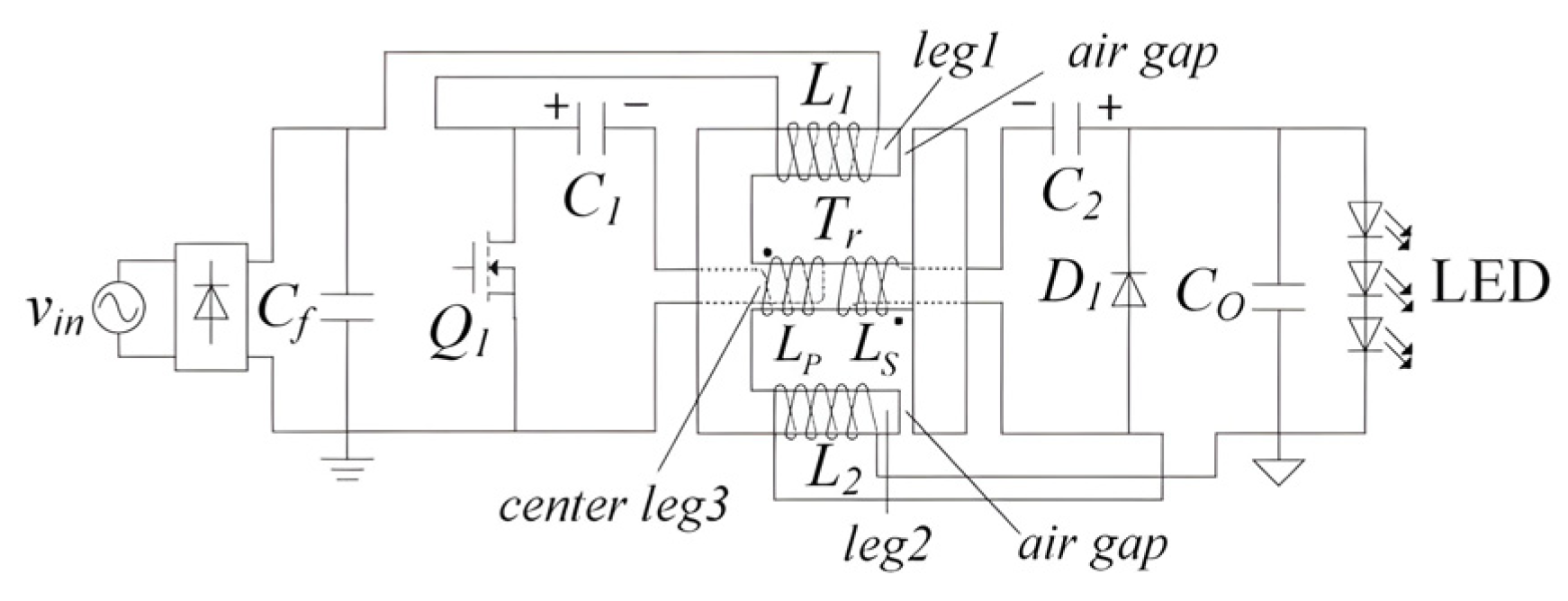
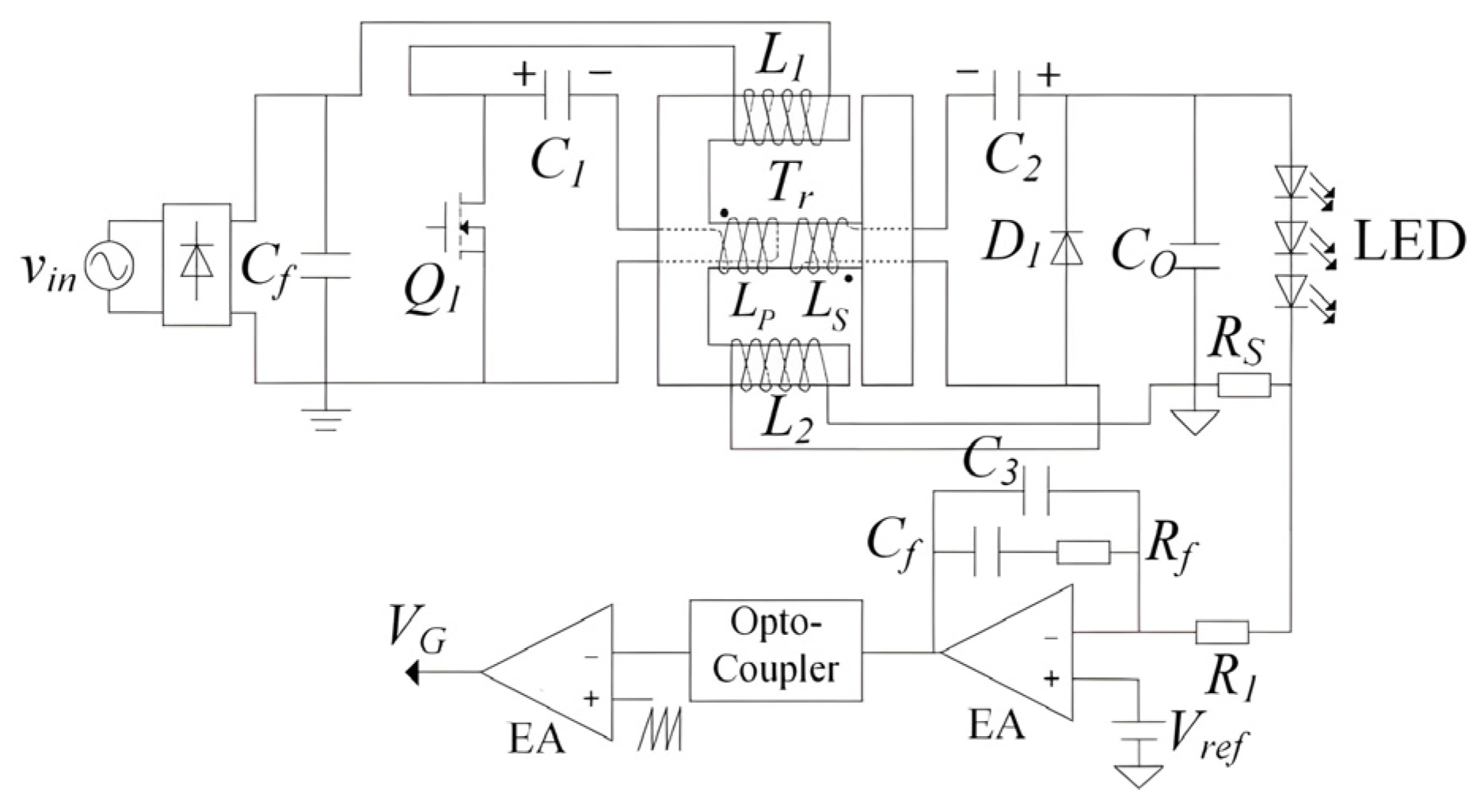
Figure 1 shows the circuit configuration of the proposed flicker-free LED driver based on isolated Cuk converter with integrated magnetic technique. The isolated Cuk converter includes switch
Q1, inductors
L1 and
L2, the coupling capacitors
C1 and
C2 with large voltage ripple, diode
D1, transformer
Tr in which
LP and
LS are the primary and secondary inductance of the transformer, and LED load. The transformer
Tr is introduced to separate the input and output. The two inductors and the transformer are wound on an EI magnetic core to achieve magnetic integration. In the proposed circuit, the transformer wire is wound around the center leg3, and two conductors’ wire are wound around the two side leg—leg1 and leg2 with a very small air gap. Mutual inductance exists between the two inductors by this method and ensures decoupling integration between the two inductors and the transformer. Due to the mutual inductance, the voltage can be shared and the voltage on the inductors can be reduced [
19,
20]. Then the twice-line-frequency LED current ripple of the LED driver based on the Cuk converter with integrated magnetics can be greatly reduced.
Compared with Buck-Boost converter and SEPIC converter, Cuk converter has the following advantages.
Both input and output are connected to inductors, making both input and output currents continuous and the pulsating currents of both are small, which is convenient for filtering at the input and output.
The output voltage of Cuk converter can be larger or smaller than the input voltage, which increases the application range of the converter.
The Cuk converter has better anti-interference performance because the switching tube short-circuits the interference at the input during the switching tube conduction and the diode short-circuits the interference at the input during the switching tube turn-off.
If the input inductor and output inductor are integrated into one core, the output ripple can be reduced by half, and by choosing a suitable inductor value or increasing the operating frequency of the converter, the output current can theoretically achieve zero ripple.
The circuit operates in continuous conduction mode (CCM) because the Cuk CCM inverter has a medium power capacity, ability to step up or down, and low input/output current ripples [
21]. The flicker-free LED driver is operated in two modes based on its operation principle: (1)
Q1 switched on and
D1 switched off and (2)
Q1 turned off and
D1 turned on.
Figure 2 shows the equivalent circuit of proposed LED driver in each mode of operation.
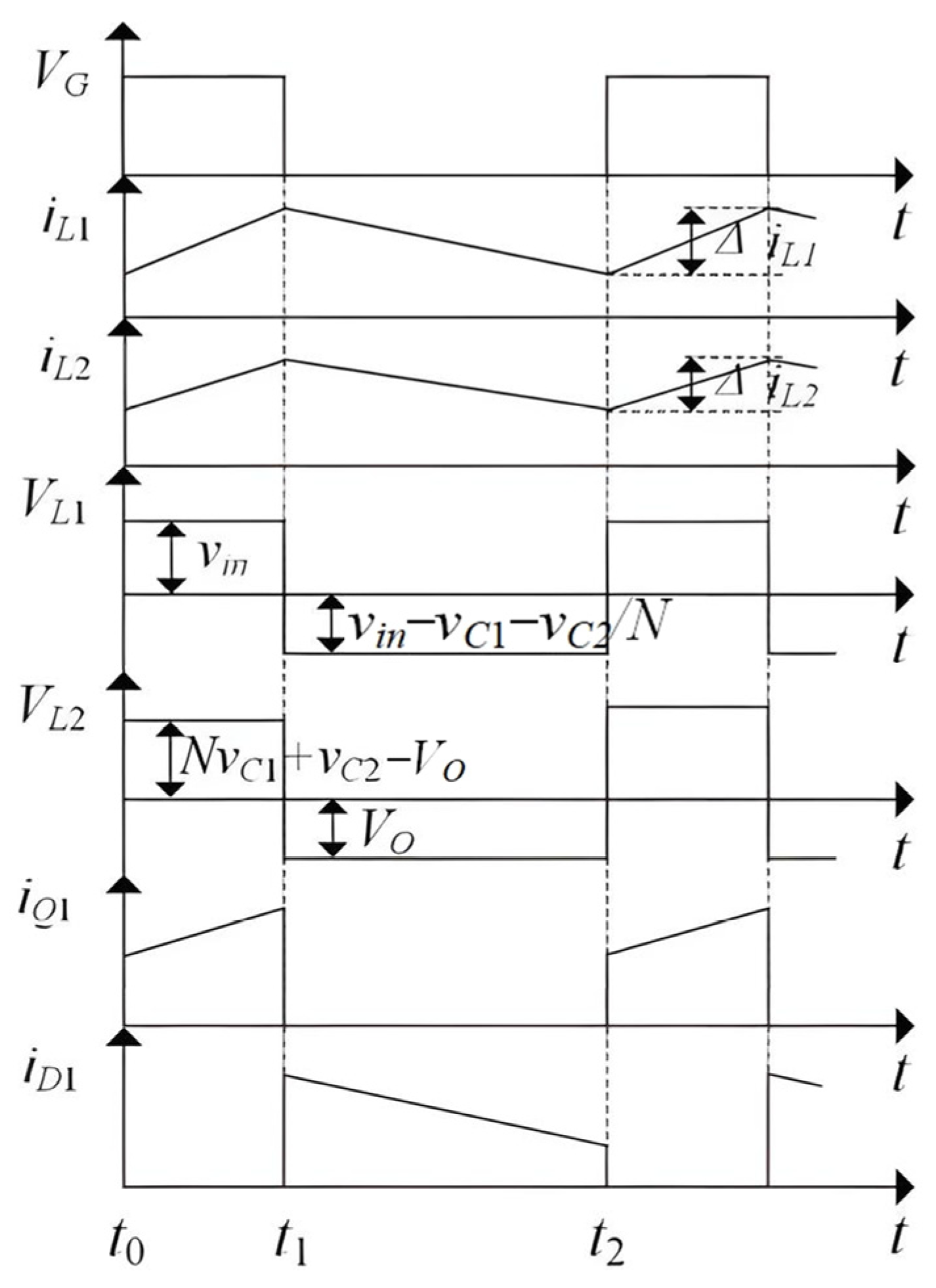
Figure 3 shows the key voltage and current waveforms.
To simplify the analysis process, the following assumptions are made:
All electronic devices are ideal, ignoring their parasitic parameters.
The switching frequency fS is much larger than the grid frequency fL, that is to say the input voltage is approximately constant over a switching period;
Capacitors C1, C2, and CO are large enough to keep the voltage constant approximately;
Since the decoupling integration mainly affects the volume and loss of the magnetic components, the influence on voltage and current is very small, the interaction between the inductors and the transformer can be neglected.
Mode1 [
t0–
t1]: At
t0, the switch
Q1 is turned on and diode
D1 is turned off because of the reverse voltage. The equivalent circuit is shown in
Figure 2a. The voltage on the inductor
L1 is input voltage
vin and it is charging during this period. The voltage on the primary winding
NL is equal to the voltage of the capacitor
C1. At the same time, the voltage induced by the secondary winding
NS and capacitor C
2 supplies to LED load together. The current flowing through
L2 increases and
L2 stores energy. According to
Figure 2a, the equation can be expressed as
where
VL1 and
VL2 are the voltages on the
L1 and
L2 respectively,
VC1 and
VC2 are the voltages on the
C1 and
C2 respectively,
M is the mutual inductance between
L1 and
L2,
N = NS/NP is the transformer turns ratio.
Mode2 [
t1–
t2]: At
t1, the switch
Q1 was turned off and diode
D1 was turned on to provide an afterflow for
LS and
L2. At this time,
L1 is discharging and provides energy to
C1. Meanwhile, the voltage induced by the secondary winding is charging
C2 through
D1. L2 provides energy to LED load through
D1 as well. According to
Figure 2b, the equation can be expressed as
According to the volt-second balance for the inductors (
L1,
L2) over a switching period
TS, we can get
where
D is the duty ratio of the switch
Q1.
The relationship between the input and output voltage can be expressed by the equation
Substituting (1) and (3) into (4), the ripple currents can be derived as
where Δ
iL1 and Δ
iL2 are the increment of
iL1 and
iL2 from
t0 to
t1.
From Equation (5), it is shown that if M = NL1, the ripple current of the inductor L2 reaches zero, and the input current iL1 remains the same as the case of no coupling. Therefore, the output current ripple is only related to inductor L1, the mutual inductance M between two inductors, and the transformer turns ratio N. The mutual inductance M is an intrinsic parameter between the coils and related to the turns of the inductors, the dimension, the position, and the magnetic medium. Anyhow, the output current ripple can be much smaller than that of the discrete magnetics.
Therefore, according to the above working principle, the twice-line-frequency LED current ripple of the LED driver based on Cuk converter with integrated magnetics can be reduced greatly.
3. Critical Design Parameter
In this section, the critical design parameters of the proposed LED driver is discussed.
3.1. Inductors L1 and L2
As mentioned in
Section 1, the LED driver is devised to operate in full CCM. Therefore, the design of the inductors
L1 and
L2 must ensure this operating condition so that all the relationships established in the theoretical analysis are valid. From (4), we have
In order to achieve high power factor, the maximum ratio of the current ripple through
L1 is chosen as 20%. According to the increase of
iL1 from
t0 to
t1, the expression is shown in (7)
where
η is the efficiency of LED driver,
PO is the power of LED,
TS is the switching period of
Q1 and
TS = 1/
fS.
Substitute (6) into (7) yields
The average current flowing through the filter capacitor
CO is zero in a grid period, so the current flowing through the LED load is equal to the current flowing through
L2 and the maximum ratio of the current ripple through
L2 is chosen as 5%. The expression is shown in Equation (9)
Substitute (6) into (9) yields
3.2. Capacitors C1, C2, and CO
The charging and discharging current of the filter capacitor
CO equal to the current ripple of
L2, which results in the voltage ripple on
CO. The equation of output voltage ripple is shown as (11).
The maximum voltage ripple on
CO is 0.1
VCOCombining (11) and (12), the restriction of design
CO is obtained as
Capacitors
C1 (is equal to
C2) transfers energy from input to output and in order to balance the instantaneous input and output power, the maximum voltage ripple on
C1 (or
C2) is 0.5
VC1 (or 0.5
VC2). The computational procedure is same as
CO.
In practical design,
C1,
C2, and
CO are CBB capacitor because of low loss, low absorption coefficient, good frequency characteristic, good self- healing effect, and high reliability [
22].
3.3. MOSFET Q1 and Diode D1
The maximum current flowing through Q1 is at the moment before Q1 is turned on and equals to the sum of IL1 and IC1. The calculation procedure of IQ is as follows.
The maximum voltage applied on the power switch transistor Q occurred at the moment after Q is turned on. The calculation procedure of VQ is as follows.
The design procedures of the current flowing through
D1 and voltage applied on
D1 are similar to that of transistor Q. According to the above analysis, the circuit specifications and parameters designed in this paper are listed in
Table 1.
4. Small-Signal Analysis and Controller Design
While the steady-state analyses define the DC status of the proposed circuit, the small-signal analysis is helpful in understanding the dynamic behavior of the integrated magnetic technique in the LED driver, and therefore, in determining the design criteria for a suitable controller and compensator. The state-space averaging method is a typical small-signal modeling and analysis method for power converters [
23]. Compared with magnetic path-electric circuit paring transformation and gyrator-capacitor equivalent model [
24], the magnetic-electrical circuit synthesis time domain model has one state variable less than the above two modeling methods, which greatly simplifies the derivation process of solving the transfer function with multi-order determinant [
25]. Therefore, magnetic-electrical circuit synthesis time-domain model is suitable for establishing a small signal model of the isolated Cuk converter with integrated magnetic technique.
There are various methods for modeling switching converters, such as current injection equivalent circuit method, state space averaging method, switching element averaging model method, and switching network averaging model method. Among them, the state-space averaging method is to select the voltage or current parameters of the nonlinear components to derive a model independent of the switching frequency, which provides more intuitive input and output characteristics and is more physically meaningful. Therefore, the state-space averaging method is selected for the derivation and analysis of the small-signal model in this paper.
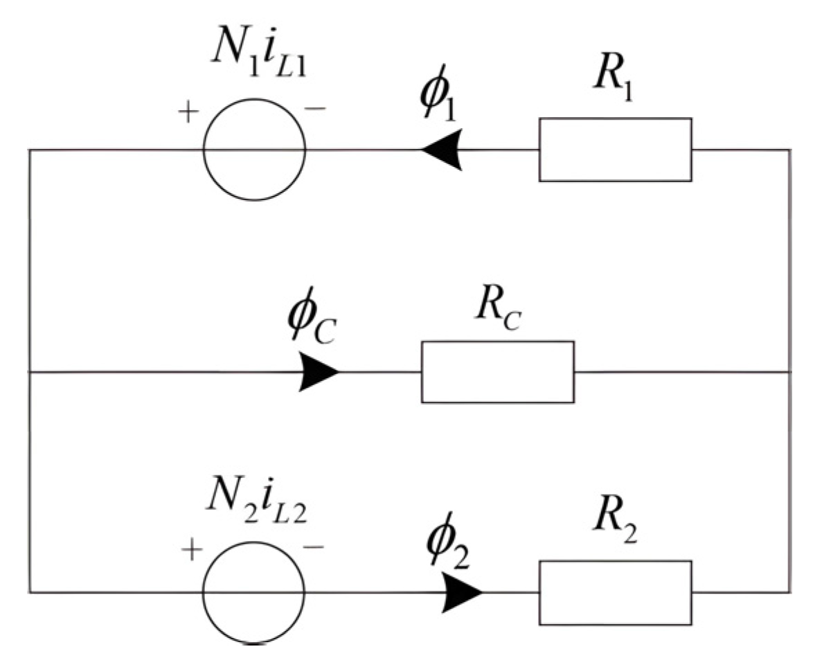
The reluctance model of the Cuk converter with integrated magnetic is shown in
Figure 4. The
L1 is around the upper side leg1 with
N1 turns of conductor, the magnetic flux is
φ1, the reluctance is
R1; the
L2 is wound on the lower side leg2 with
N2 turns of conductor, the magnetic flux is
φ2, the reluctance is
R2; the primary and secondary side of the transformer are wound in center leg3 with the magnetic flux
φC and the reluctance
RC. Thus, according to Ohm’s law based on the magnetic circuit, we can get the following equation:
According to the continuity of magnetic flux,
φ1 =
φ2 +
φC, then (6) can be rewritten as
Select state vector
x(
t) in the proposed Cuk converter as [
ϕ1(
t)
ϕ2(
t)
vO(
t)
vC1(
t)
vC2(
t)]
T, the input variable
u(
t) is [
vin(
t)]
T, the state-space equation in mode 1 can be expressed as
The findi Rewrite (8) as
=
Ax(
t) +
Bu(
t), then
A1 and
B1 can be expressed as follows ngs and their implications should be discussed in the broadest context possible. Future research directions may also be highlighted.
Similarly, the state-space equation in mode 2 can be expressed as
The corresponding matrix
A2 and
B2 are
Using the state-space averaging method, then we get the transfer function in the form of Laplasse transform and the small signal model is derived as follows:
where
is the proportion of mode 2.
Based on the above small-signal model, the duty- ratio-to-output-voltage transfer function
Gvd (
s) can be expressed as
where the derived parameters
ai(
I = 1, 2, 3, 4) and
bj(
j = 1, 2, 3, 4, 5, 6) are omitted for brevity.
In the model, the reluctance
R1 is 9.5 × 10
9 A·t/Wb, reluctance
R2 is 1.27 × 10
10 A·t/Wb, reluctance
RC is 1.14 × 10
10 A·t/Wb. Finally, we can calculate the
Gvd(
s) based on MATLAB with the parameters in
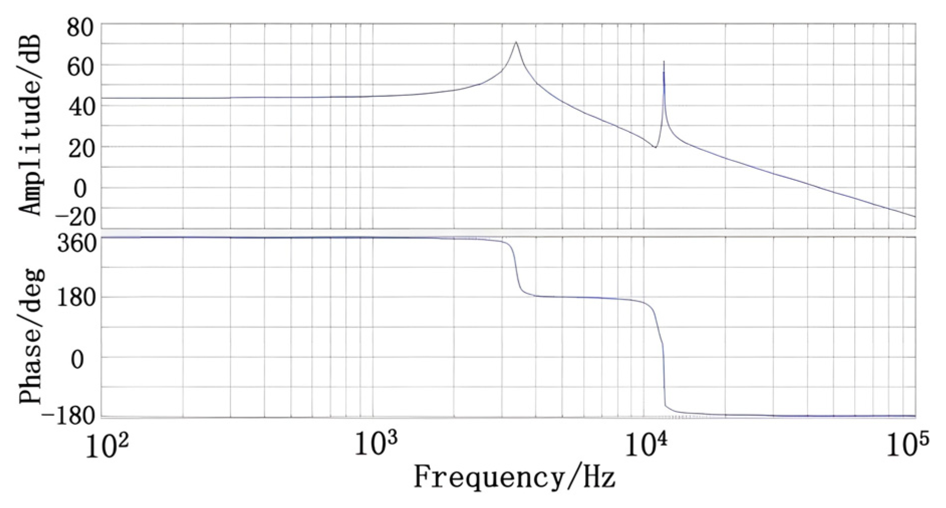
Table 1. The Bode diagram of
Gvd(
s) is shown in
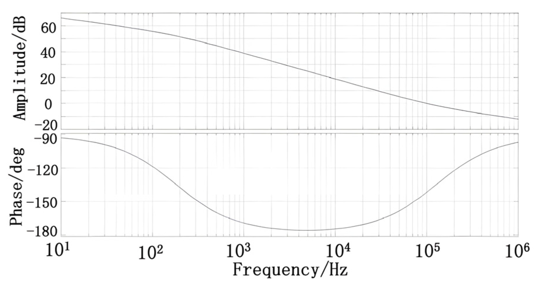
Figure 5.
According to the Bode diagram, there are two low-frequency resonance points f1 = 3.2 kHz and f2 = 10.4 kHz and one zero resonance point f3 = 10.6 kHz. The zero resonance point at f3 balances the pole at f2, so there is no resonance peak in the Bode diagram, the circuit phase lags by 180 degree and its amplitude-frequency characteristic is declining by 40 dB/dec. Therefore, to make the circuit stable when wide range input voltage, phase compensation circuit should adopt the type II feedback network.
Figure 6 shows the circuit diagram of a typical type II feedback network. In order to realize quick regulation and high PF, the voltage-mode control is adopted. The compensator transfer function is
where
,
,
.
In this compensator design, the circuit parameters are R1 = 51 kΩ, Rf = 270 kΩ, C3 = 680 pF, Cf = 470 nF.
According to classical control theory, an ideal control system should have the following characteristics.
The low frequency band decreases at a slope of −20 dB/dec and has a certain height to ensure that the requirements of steady-state accuracy are met, followed by a slope of −40 dB/dec to increase the rapidity of the system.
The middle frequency band should ensure that the cut-off frequency is large enough to meet the requirements of dynamic rapidity, and the amplitude-frequency characteristic curve at the 0 dB line should cross at −20 dB/dec and maintain a certain width to meet the requirements of the relative stability of the system.
The amplitude-frequency characteristic curve of the high-frequency band should have a large negative slope, generally less than or equal to −40 dB/dec to improve the system’s ability to resist high-frequency interference.
Figure 7 shows the Bode diagrams of the proposed compensator. It can be observed that ratio is −20 dB/dec in low frequency, −40 dB/dec in medium frequency, and −20 dB/dec in high frequency, which are the key characteristic according to classical control theory.
5. Simulation and Results Analysis of Proposed LED Driver
The Saber software was used to simulate the Cuk circuit with integrated magnetics. A resistance was used instead of the LED. The parameters are listed in
Table 1. All the diodes are ideal.
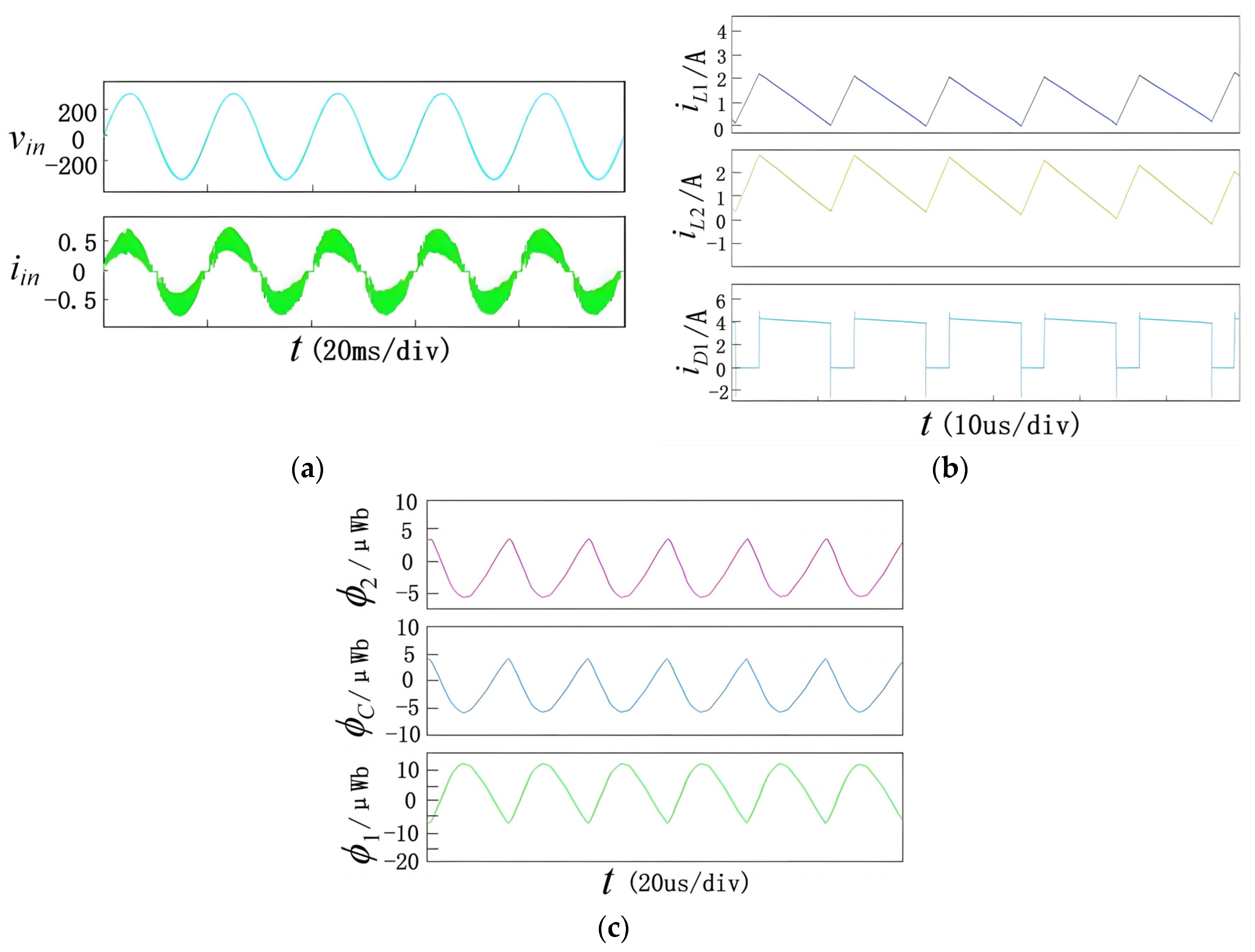
The simulation results of the magnetic integrated circuit are shown in
Figure 8.
Figure 8a shows the waveforms of input voltage
vin and input current
iin. It can be seen that the input voltage and current are nearly in the same phase, so the driver achieves unity power factor.
Figure 8b shows the waveforms of the inductor current
iL1,
iL2 and diode current
iD1. It can be seen that the circuit works in CCM mode.
Figure 8c gives the flux curves of the three legs. Obviously,
φ1 +
φ2 +
φC = 0, which is exactly the same as the theory.
In order to verify the proposed flicker-free LED driver, a prototype has been built and tested in the laboratory. Beside the parameters listed in
Table 1, other specification of the prototype is as follows: the load is three strings of 10 × 1 W LED, the core of transformer adopts the EI-shaped ferrite magnetic, power switch
Q1:SPW20N60C3; free-wheeling diode
D1: HFA25TB60S; control IC: UCC3844.
The bridgeless Cuk converter studied in this paper is a small to medium power circuit, and the switching tubes used are MOSFETs, whose maximum current withstand value occurs at the moment of transition from mode 1 to mode 2. At the same time, the switch tube withstand voltage value needs to be considered to leave twice the margin. The above selection conditions were combined to select the Infineon SPW20N60C3 model with a drain breakdown voltage of 650 V, on-state resistance, and continuous drain current of 20.5 A (25 °C). The voltage stress of the diode is the same as the voltage of the switching tube, so the actual circuit should be left with more than twice the margin, the comprehensive selection of the international rectifier company HFA25TB60S. The UC3842 is a high-performance fixed-frequency current-mode PWM integrated controller from TI that uses a minimum of external components to achieve PFC correction and an internal high-current totem pole output of ±1 A, making it an ideal device for driving power MOSFETs.
In addition, the filtering electrolytic capacitors required by the converter can be replaced by film capacitors or ceramic capacitors to some extent. Compared with electrolytic capacitors, film capacitors have the advantages of long life, high stability, good temperature characteristics, high voltage-withstanding capability, and low loss in high frequency, while ceramic capacitors have better high-frequency characteristics and can play the role of coupling, filtering, and oscillation in high-frequency circuits. Therefore, the use of film capacitors or ceramic capacitors can reduce the system loss and maintenance cost, while not affecting the size of the system.
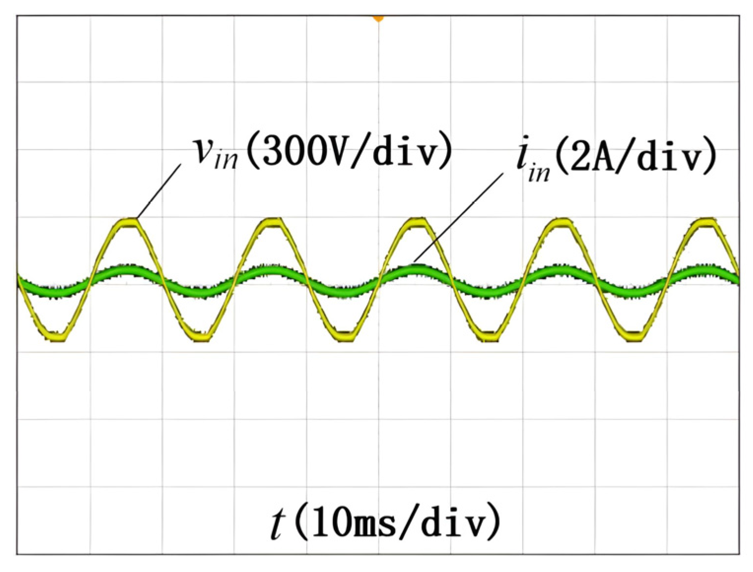
Figure 9 shows the waveforms of input voltage
vin and current
iin. The input current follows the voltage change and achieves high power factor. The measured PF value is 0.982.
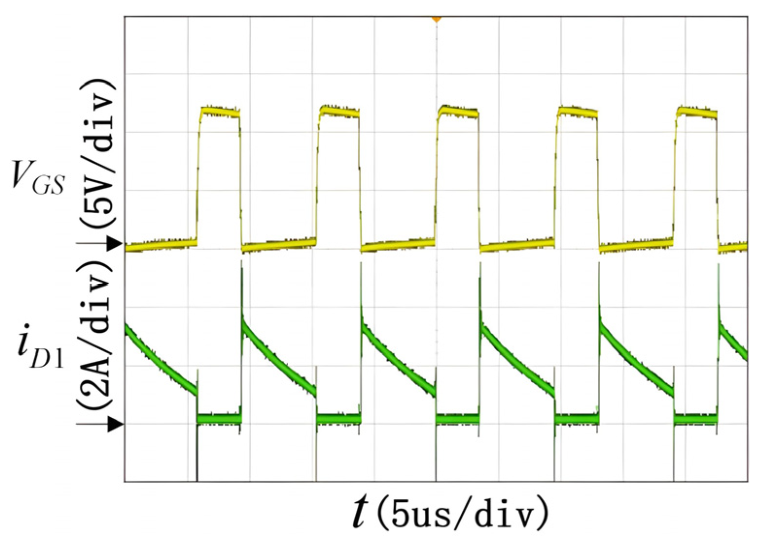
Figure 10 shows the waveforms of switching signal VGS and the freewheeling diode current iD1. The switching frequency is presented as 100 kHz and the duty ratio D is 31%. The freewheel diode operates in CCM mode, which is exactly the same as the theoretical analysis.
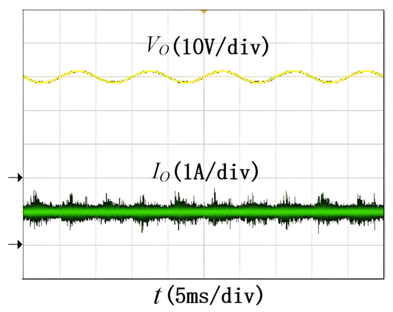
Figure 11 shows the waveforms of filter capacitor voltage
VO and LED current
IO. The filter capacitor voltage contains AC component with twice the line frequency, but the LED current is a pure DC current, thus it basically eliminates the LED flicker.
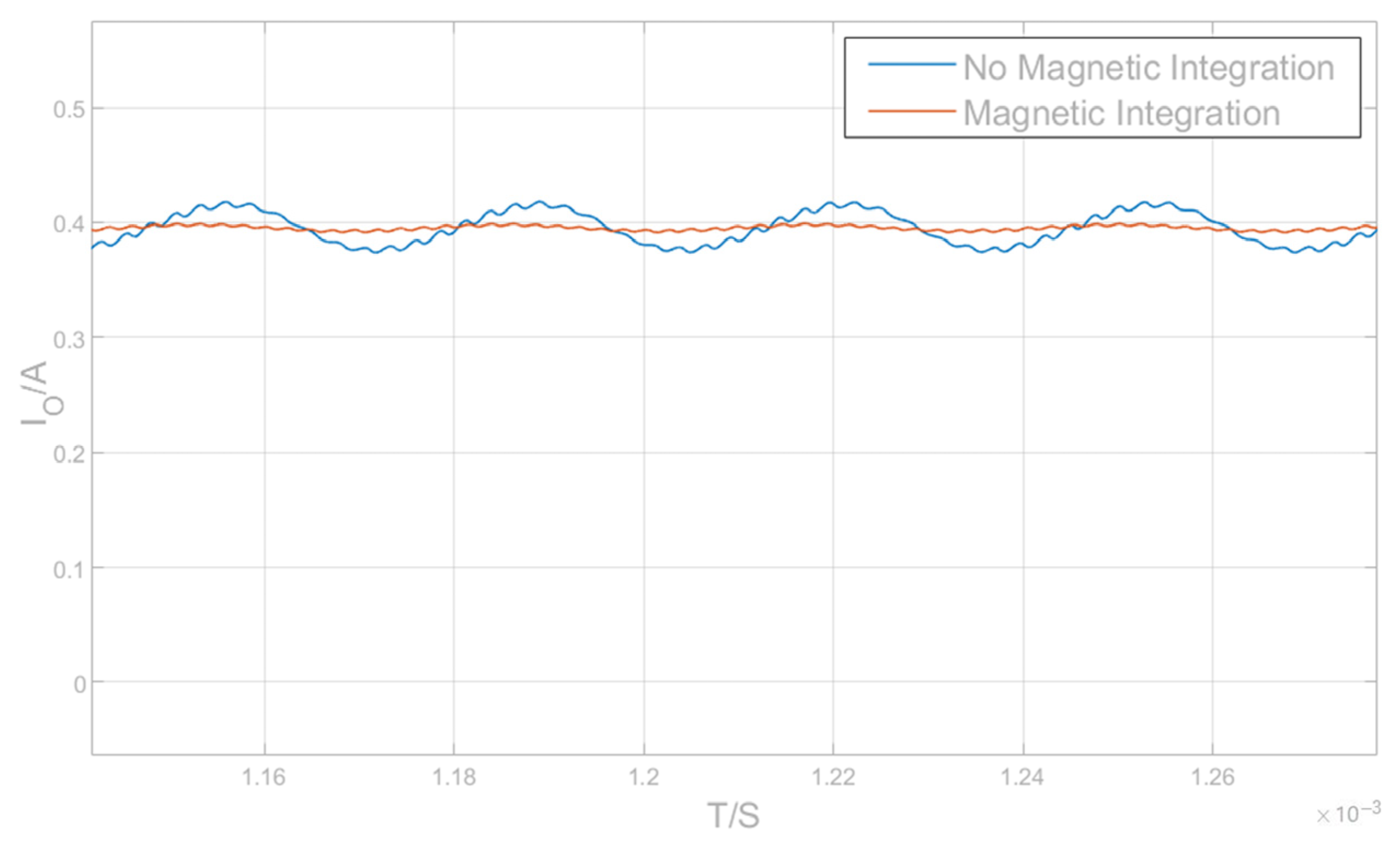
Figure 12 shows a comparison of the system output current before and after the adoption of the magnetic integration technique. It can be seen that the system output current ripple is significantly reduced after adopting the integrated magnetic technology.
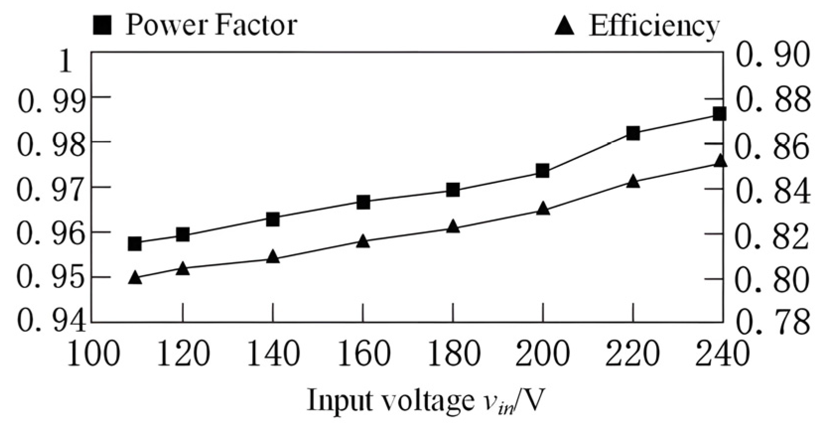
Figure 13 shows the relationship between the PF value and the efficiency of the flicker-free LED driver with different input voltage, respectively. From
Figure 13, it can be seen that the PF value is always above 0.95 and the maximum efficiency is 0.838 over the entire input voltage range. The difference between the theoretical prediction and the experimental results occurs mainly due to the efficiency of the converter, which varies according to the input voltage.
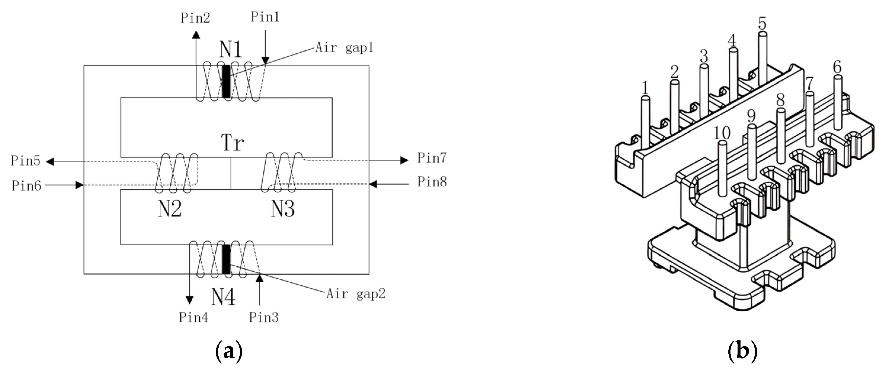
Figure 14 illustrates the winding method of the coil and transformer to form an integrated magnetic element, and the pin-out figure of the element.
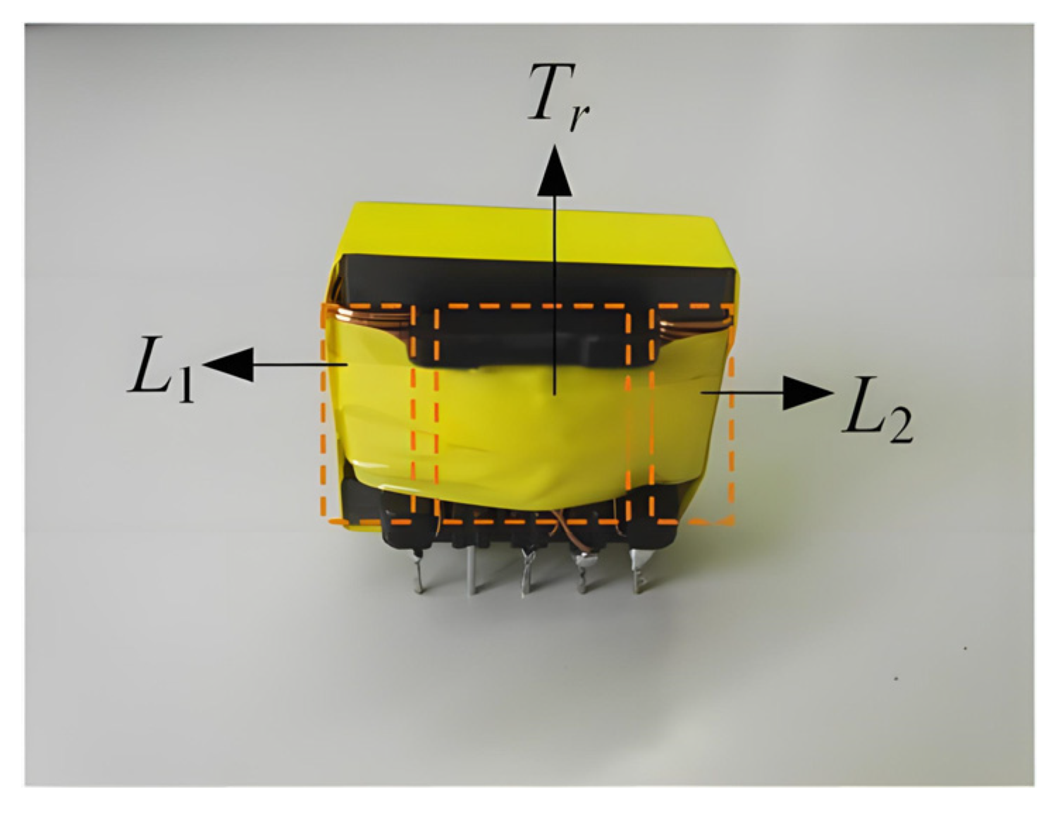
Figure 15 shows the photo of the magnetic integrated inductance L1, L2 and transformer Tr.
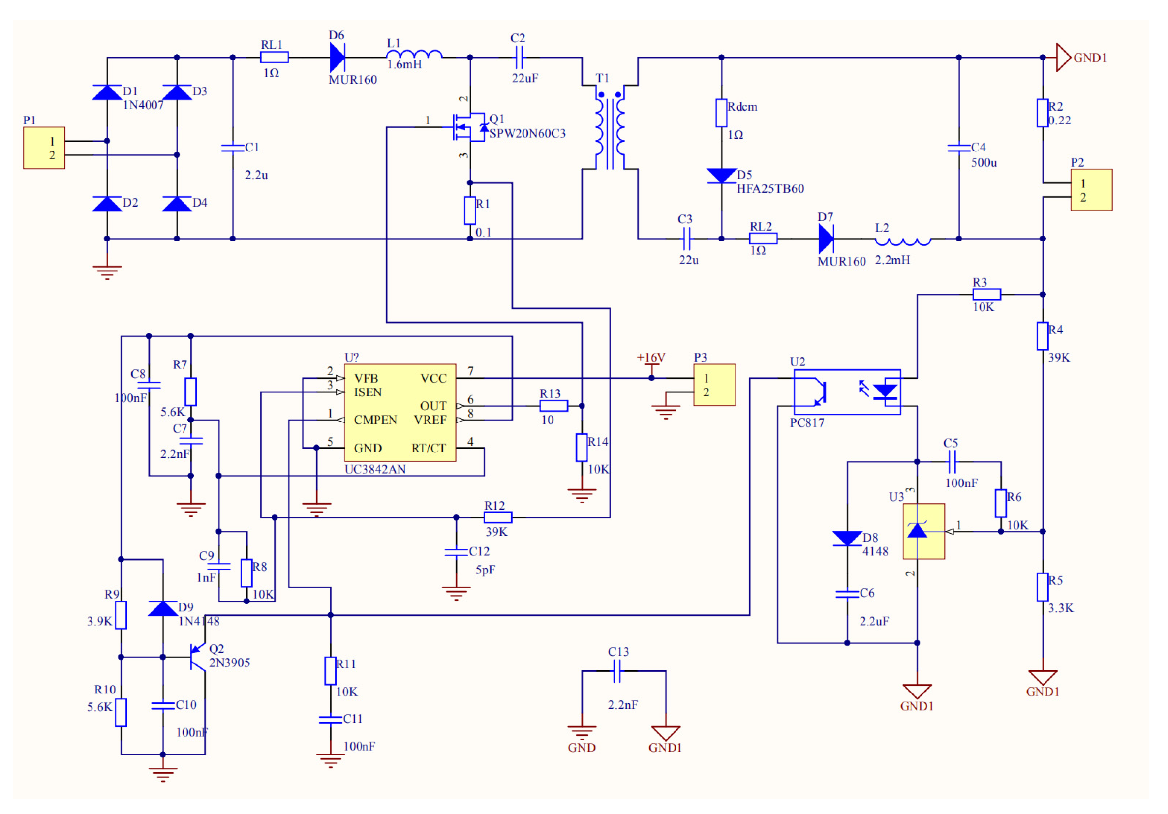
Figure 16 shows the system circuit diagram.
The LED driver proposed in this paper reduces the cost of the system mainly through the following two aspects. First, in terms of component selection, film capacitors or ceramic capacitors can be used instead of the commonly used filtering electrolytic capacitors, which not only improves the system operating performance, but also saves component turnover and reduces system maintenance costs. Second, most current pulsating current elimination methods need to rely on complex control loops or require the provision of additional DC power supplies, etc. These methods more or less enhance the cost of building LED drivers. This paper proposes to integrate two inductors and isolation transformers in one core, which can make the maximum working magnetic density of the integrated magnetic parts much smaller than the magnetic density of each discrete magnetic parts and thus achieve the purpose of reducing the cross-sectional area of the magnetic parts core and reducing the cost and volume of the magnetic parts. At the same time, this approach does not need to rely on the above-mentioned measures to enhance system cost to achieve zero current ripple.
The converter efficiency can be improved by means of improving the magnetic concentration elements. There are two main types of methods to improve the magnetic concentration element with the main purpose of improving efficiency. The first type is to cut the AC fluxes to each other in the common column, which largely reduces the alternating magnetic density and at the same time reduces the loss of the magnetic core. There are three main ways: (1) Changing the winding connection and changing the coupling of fluxes; (2) merging the windings according to the specific circuit; (3) splitting the windings with the source transfer equivalent transformation method. The second type is the mutual superposition of AC flux and DC flux, which can improve the core utilization.
6. Conclusions
This paper presents a 30 W flicker-free LED driver prototype that uses magnetic integration technique to eliminate stroboscopic effect in an isolated Cuk converter. The operation principle of Cuk converter with integrated magnetics is analyzed in detail using time domain analysis in electrical and magnetic circuits. The transfer function Gvd (s) is calculated and the Bode diagram is drawn. Based on simulation and experimental results, the flicker-free LED driver has a power factor of 0.982 and a maximum efficiency of 0.838 when the input voltage is 240 V and LED current is pure DC current. The proposed driver is small-sized and cost-effective due to the use of only one transformer core. Future research will focus on improving the efficiency by analyzing the loss distribution of the magnetic integrated LED driver and applying a soft switching circuit and improved magnetic integrated element.


