Article

Study on Tungsten Metallization and Interfacial Bonding of Silicon Nitride High-Temperature Co-Fired Ceramic Substrates

1
Center of Materials Science and Optoelectronic Engineering, University of Chinese Academy of Sciences, Beijing 100049, China
2
State Key Laboratory of High Performance Ceramics and Superfine Microstructures, Shanghai Institute of Ceramics, Chinese Academy of Sciences, Shanghai 200050, China
3
School of Materials and Chemistry, University of Shanghai for Science and Technology, Shanghai 200093, China
*
Author to whom correspondence should be addressed.
Materials 2023, 16(7), 2937; https://doi.org/10.3390/ma16072937
Submission received: 18 March 2023 / Revised: 1 April 2023 / Accepted: 4 April 2023 / Published: 6 April 2023

Abstract

:
For the first time, Si3N4 HTCC has been prepared using W as the metal phase by high-temperature co-firing (1830 °C/600 KPa/2 h) as a potential substrate candidate in electronic applications. It was discovered that the addition of Si3N4 to the W paste has a significant impact on thermal expansion coefficient matching and dissolution wetting. As the Si3N4 content increased from 0 to 27.23 vol%, the adhesion strength of W increased continuously from 2.83 kgf/mm2 to 7.04 kgf/mm2. The interfacial bonding of the Si3N4 ceramic and the conduction layer was discussed. SEM analysis confirmed that the interface between Si3N4 and W exhibited an interlocking structure. TEM, HRTEM and XRD indicated the formation of W2C and W5Si3 due to the interface reactions of W with residual carbon and Si3N4, respectively, which contributed to the reactive wetting and good adhesion strength between the interface. Suitable amounts of Si3N4 powder and great interfacial bonding were the main reasons for the tough interfacial matching between the Si3N4 ceramic and the conduction layer.

1. Introduction

High-temperature co-fired ceramic (HTCC) is a multilayer ceramic circuit board made from conductive metal paste printed on the ceramic substrate through screen printing according to the circuit design requirements. HTCC is characterized by its high structural strength, good thermal conductivity, excellent chemical stability and high wiring density. Aluminum oxide (Al2O3) and aluminum nitride (AlN) have been widely used as substrates of HTCC for electronic devices [1,2]. As the most mature ceramic substrate material, Al2O3 has many advantages as a low-power electronic device substrate material, such as its low dielectric loss, excellent mechanical strength, low preparation cost, etc. [3,4,5,6]. However, the thermal conductivity of Al2O3 ceramics is too low to meet the heat dissipation requirements for high-power transmission [4]. Metallization based on AlN was carried out in the early 21st century, and now it has been applied in the military and other industries [7,8,9]. The major drawback of AlN is its low mechanical properties and chemical stability [10]. On the other hand, silicon nitride (Si3N4) possesses high strength [11], toughness [12], heat shock resistance [13], a high dielectric constant [14] and other characteristics, making it a suitable substrate material for high-power and high-density electronic devices [15,16]. In addition, as the substrate of high-power electronic devices, Si3N4 HTCC not only needs to provide mechanical support and excellent heat dissipation ability but also electrical interconnection for the integrated electronic devices on it. This requires a good combination of the Si3N4 and the metal circuit, as well as good electrical conductivity of the metal circuit. As the substrate material of HTCC, it has shown broad application prospects in many fields, such as the military industry, communications, environmental protection, aerospace and so on [17].
A Si3N4 material with high thermal conductivity can be successfully prepared by reaction bonding and post-sintering with the aid of rare earth oxide and alkali metal oxide [18,19]. Therefore, Si3N4 could be used as the substrate of high-power electronic devices with the solution of metallizing Si3N4 ceramic. However, there are still few reports on the metallization of Si3N4 ceramic for applications in electronic devices internally [20,21].
Starting in 1956, La Forge first carried out metallization experiments on Al2O3 with the activated Mo-Mn method. Then, Reed [22], Fulrath [23] and Twentyma [24] et al. further optimized the experiments. However, the sintering temperature is still too low to densify Si3N4. The tungsten co-firing method, utilizing tungsten with a high melting point of 3400 °C, is a crucial factor in achieving successful sintering of AlN HTCC above 1700 °C. Song et al. improved the AlN tungsten mentalization and prepared AlN HTCC with an adhesion strength of 2.95 kgf/mm2 and a conduction layer resistance of 9.8 mΩ/sq [25]. Hu et al. discussed the role of SiO2 in tungsten paste and the electrical and mechanical properties of the substrate. SiO2 reacts with Y2O3, CaO and AlN to form crystalline phases of CaSiAlO and YSiO and vitreous Y-sialon and Ca-sialon at the interface of the substrate and the conduction layer. The conduction layer resistance of the multilayer co-fired substrate is up to 10 mΩ/sq, and the adhesion strength is up to 3.15 kgf/mm2 [26]. It was found that Si3N4 is sintered at temperatures above 1700 °C in the N2 atmosphere. As is known to all, Mo reacts with N2 at temperatures up to 1500 °C and densifies below 1600 °C by the Mo-Mn method. Consequently, refractory metal W becomes a better choice. As reported in the literature [27,28], the thermal expansion coefficient of Si3N4 varies from 20 °C to 1000 °C, showing a monotonous upward trend from 1.4 × 10⁻⁶ K−1 to 4.0 × 10⁻⁶ K−1. However, the thermal expansion coefficient of W at 20 °C is ~4.0 × 10⁻⁶ K−1 and increases with rising temperatures. It can exceed 6.0 × 10⁻⁶ K−1 above 1500 °C. Therefore, in order to reduce the thermal stress after sintering, it is necessary to adjust the coefficient of thermal expansion of the conduction layer during sintering by adding Si3N4 appropriately so as to obtain a good co-firing effect.
In this study, the Si green tape was obtained by tape casting with a suitable addition of Er2O3 and MgO as sintering additives. The tungsten paste ball milling mixed with Si3N4 powder was printed on the green tape using screen printing technology. After lamination, hot pressing, debinding, nitriding and sintering, Si3N4 HTCC with a strong adhesion strength (5.25 kgf/mm2) and good film resistance (98.8 ± 20 mΩ/sq) was obtained. The microstructure, phase compositions and mechanism of the interfacial bonding were analyzed.

2. Materials and Methods

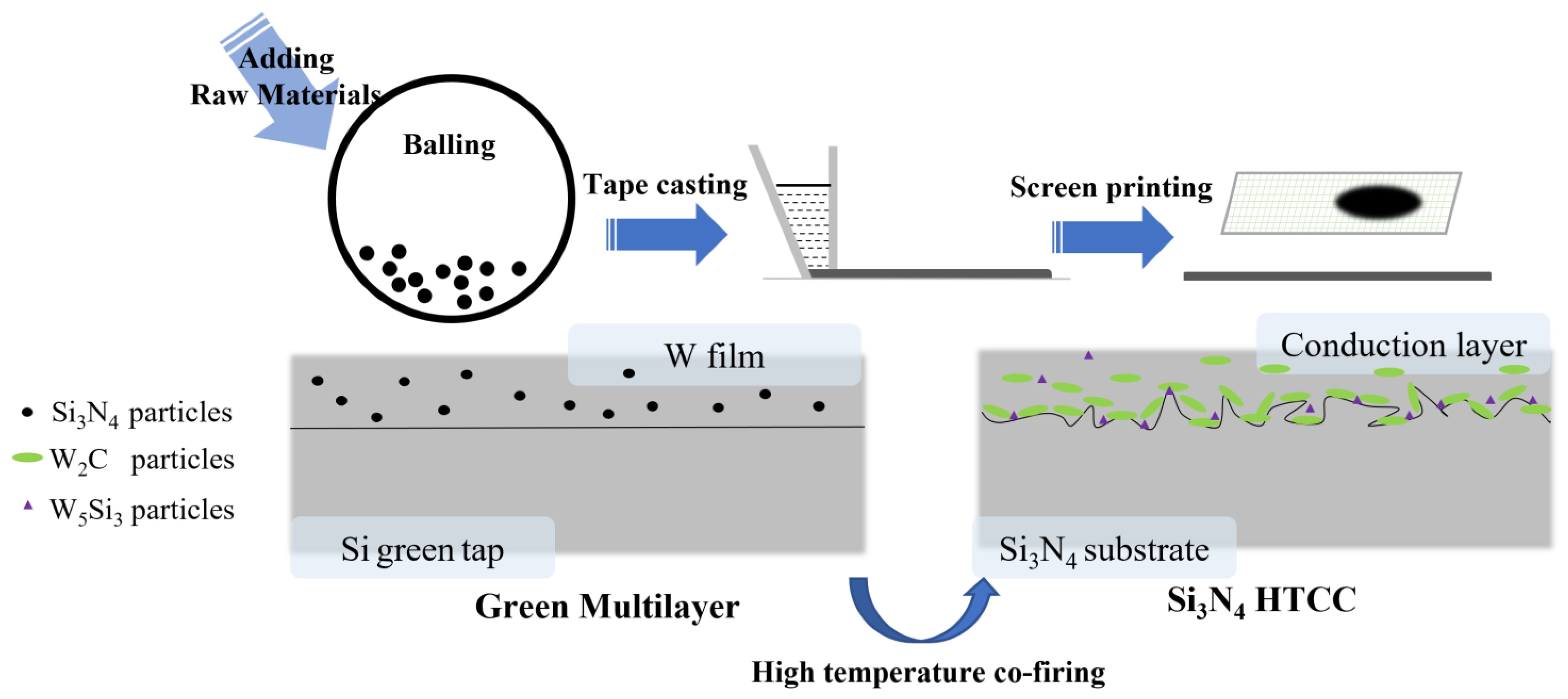
2.1. Raw Materials and Experiment Procedure

Commercial high-purity tungsten powder (W, Innochem, 99.98% metals basis, 1–5 μm, 0.26 wt% O, D50 = 3.47 μm) and Si powder (99.999%, BET 2.205 m2/g, 0.42 wt% O, D50 = 5 μm, Haoxi Research Nanomaterials, Inc., Shanghai, China) were used in the present study. High purity Er2O3 (purity > 99%, Haoxi Research Nanomaterials, Inc., Shanghai, China) and MgO (purity > 99%, Qinhuangdao Yi Nuo Co, Ltd., Qinhuangdao, China, BET 10.448 m2/g) were used as sintering additives. Si3N4 (purity > 99.5%, UBE Industries, Ltd., Kogushi, Japan, 1.26 wt% O, BET 11.6 m2/g) was selected as the additive for W paste. The composition of Si slurry with sintering additives was designated as Si:Er2O3:MgO = 88:9:3 at mass ratio. Polyvinyl butyral (PVB) was used as binder and butyl benzyl phthalate (BBP) was used as plasticizer. W-based screen printing paste with Si3N4 powders was designated as W:Si3N4:Er2O3:MgO = 64–91.23:0–27.23:5.98:2.79 at volume ratio.
The Si, Er2O3 and MgO powders with defined compositions were dispersed in mixed solvent of ethyl alcohol and xylene at 1:1 (mass ratio) and lab-made dispersant for 24 h. In order to avoid competitive adsorption between binder and dispersant, the slurry with solid loading of approximately 42% was milled after the addition of PVB and BBP for another 36 h. Then, tape casting was carried out on Procast Precision Tape Casting Equipment (Division of International, Ringoes, NJ, USA) at a speed of 120 mm/min with a thickness of 0.4 mm. The obtained green tape was used for the next screen-printing process.
In order to obtain a uniform W screen-printing paste, W, Si3N4, Er2O3, MgO and organic vehicle were mixed using a planetary mill for 4 h with WC balls as the medium in polyethylene jars. The organic carrier included ethyl cellulose as binder, span-85 as dispersant, terpineol, butylcarbitol, tributyl citrate, butylbenzyl phthalate as mixed solvent, and hydrogenated castor oil as thixotropic agent. Then, screen printing was performed by screen printer (HP-3050, Haohe Machinery, Dongguan, China) on Si green tape to produce Si/W green tape. Subsequently, after drying at room temperature for 24 h, the Si/W green tape was laminated into uniform 50 mm × 50 mm blocks by laser cutting and hot lamination (9 layers). Then, the laminated green multilayer was heat treated at 200–500 °C with N2 as the protective atmosphere to burn out the organics. Dense Si3N4 HTCC was prepared by reaction bonding and post-sintering method: nitriding at 1420 °C for 2 h under 0.1 MPa N2 and sintering at 1830 °C for 1 h 0.6 MPa N2 with heating rate of 3 °C/min. Then a slow cooling rate of 3 °C/min to 1500 °C and a second, slower cooling rate of 2 °C/min to 1400 °C with 1 h holding period were adopted.

2.2. Characterization

Thermogravimetric analysis of the green body was conducted using TG (STA449C, Netzsch) at a heating rate of 10 °C/min under the flux of air and N2 gas at a rate of 30 mL/min. The delta Gibbs energy of the reactions was calculated using HSC Chemistry (HSC Chemistry 9.0). The phase compositions were identified by X-ray diffraction (XRD, D8 Advance, Bruker, Germany) using Cu Kα. The microstructure and element distribution were characterized by scanning electron microscopy (SEM, Magellan 400, FEI Co., Hillsboro, OR, USA), energy dispersion spectroscopy (EDS, Inca of Oxford Instruments, Oxford, UK), transmission electron microscopy and high-resolution transmission electron microscopy (TEM and HRTEM, Tecnai G2 F20, FEI Electron Optics) with energy-dispersive X-ray analysis (EDAX). For TEM samples, thin foils were prepared by focused ion beam technology (FIB, Versa 3D, FEI, Hillsboro, OR, USA). The film resistance was measured using quadrupole probe method (RTS-9, 4probes Tech Ltd., Guangzhou, China).
R = ρ/d
where R (Ω/sq) represents the film resistance; ρ(Ω·m) represents the resistivity; d (m) represents the thickness of the film.
Adhesion strength was tested by vertical tensile method (GB/T 17473.4-2008) by multifunctional tension tester (DAGE4000, DAGE, Aylesbury, UK) on 2 × 2 mm2 pad electroplating Ni/Pd/Au.

3. Results and Discussion

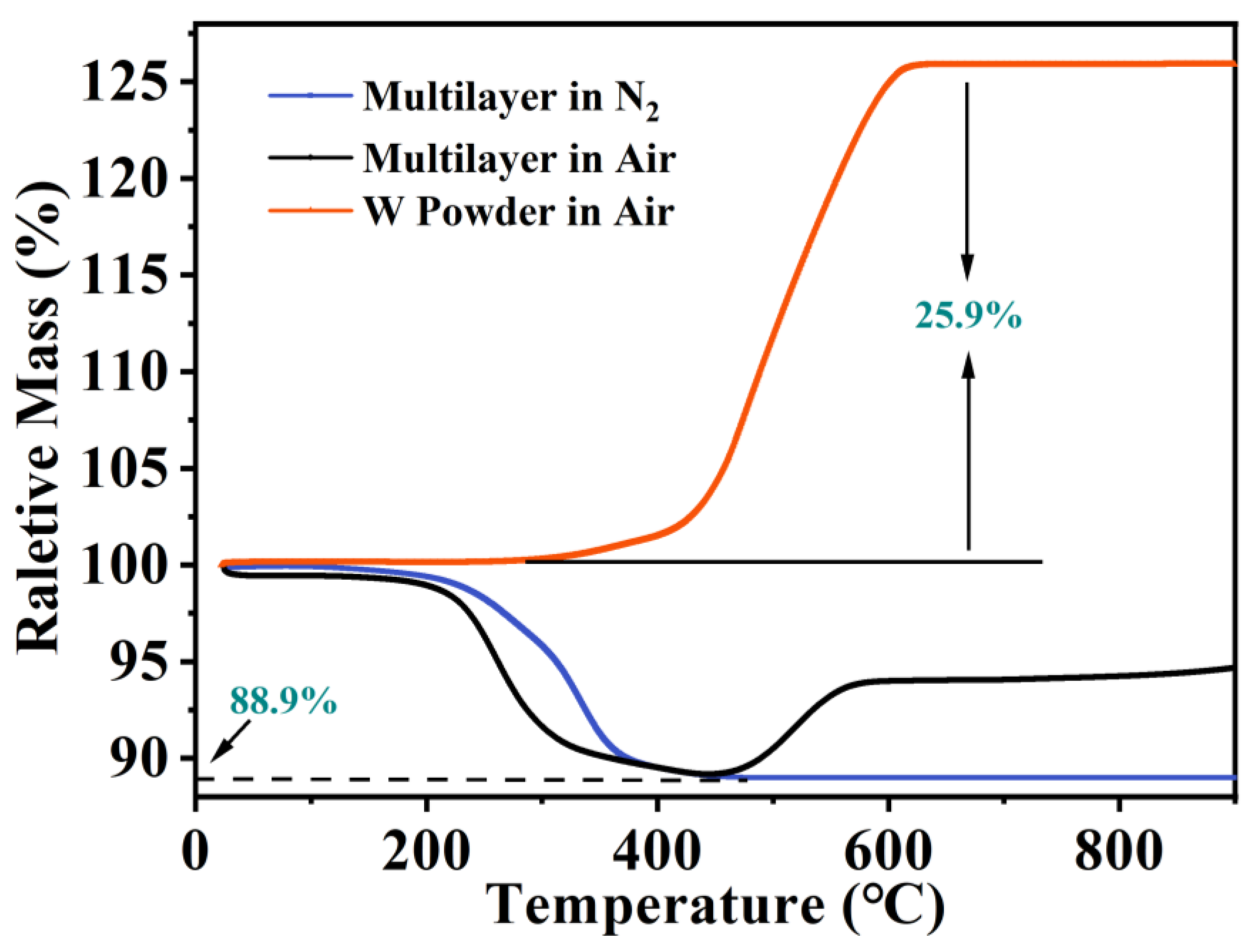
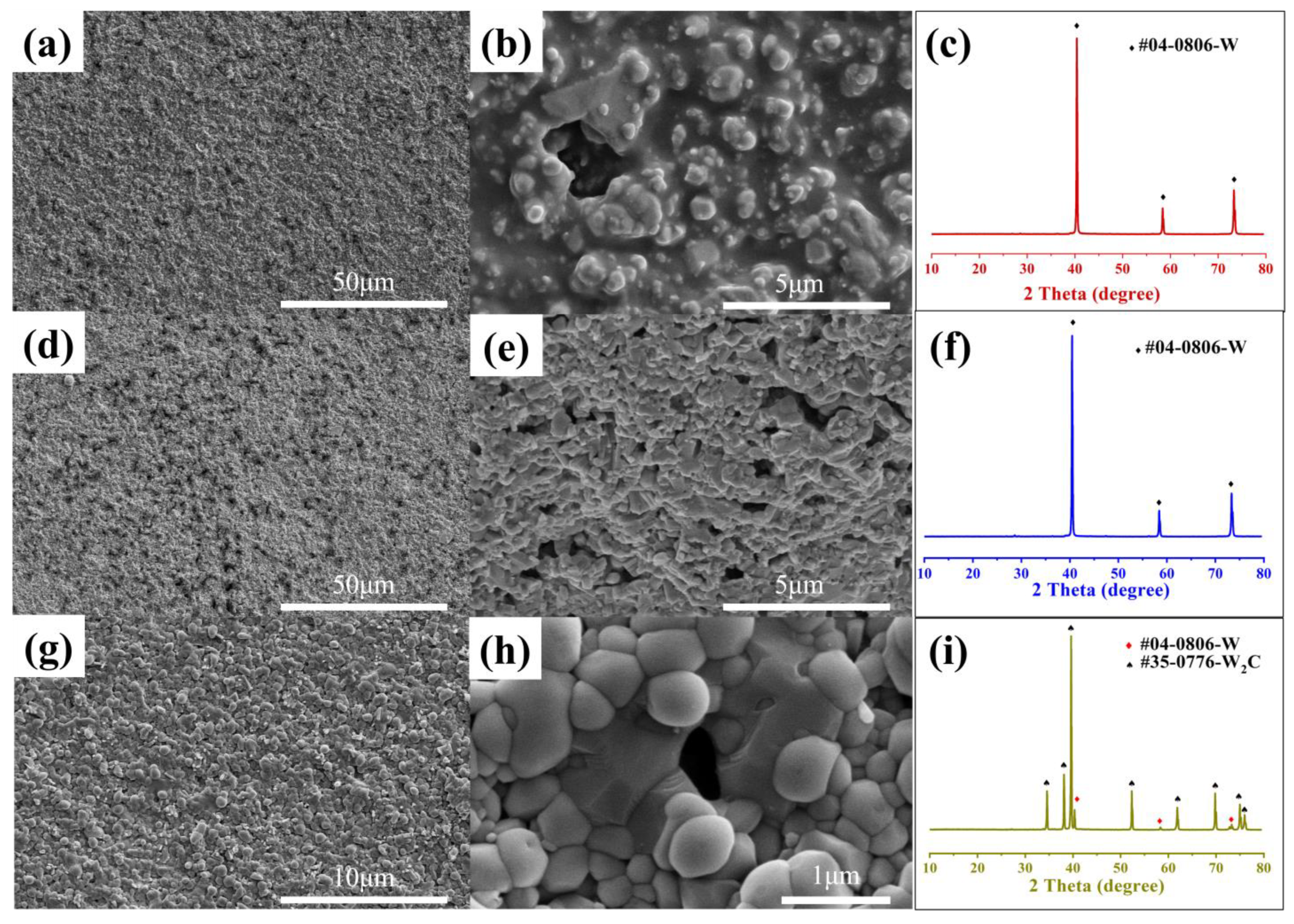
3.1. Sintering Process of Multilayer Green Bodies

Figure 1 illustrates the different thermal analysis curves of the green multilayer and W metal powder. The green multilayer was heated from room temperature to 900 °C in an air and N2 atmosphere with a heating rate of 10 °C/min. The W powder was heated from room temperature to 900 °C only in air. Prior to nitridation, the organic components in the Si3N4 multilayer were removed. As Figure 1 shows, tungsten starts to gain weight at 360 °C, and a significant increase of 25.9% is observed after increasing the temperature to 600 °C in air. The thermal analysis curve of multilayer samples in the air also shows an obvious weight gain stage, which starts at 480 °C and ends at 600 °C. This indicates that when the organics are burning in air, the W metal is oxidized, which seriously affects the film resistance performance of the metal circuit [29]. In the N2 atmosphere, the thermal analysis curve of the multilayer shows a continuous weight loss of 11.1% from 200 °C to 500 °C. To prevent oxidation of the W layer in air and issues caused by rapid organic volatilization, a debinding process was adopted with a heating rate of 1 °C/min in the nitrogen atmosphere, and multiple holding points were set between 200 and 500 °C.
SEM observations were carried out to observe the surface morphology of the samples at the green tape, after debinding and after nitriding stages. Figure 2 presents the surface morphologies and XRD curves of the samples at these three stages. The surface morphology of the green tape shown in Figure 2a,b clearly displays that W particles were well-coated by the organic film. The chemical composition of the conduction layer, as confirmed by the illustration in Figure 2a, is a W element. After debinding in N2, the organic film disappeared, as shown in Figure 2e, and there were interspaces among W particles, as depicted in Figure 2d. The diffraction intensity of W (110) was relatively high and sharpened without any miscellaneous peaks, which indicated that no side effects were observed during the debinding process. After the nitridation step, sphere-like particles with a size of around 1 μm could be seen according to the SEM observation, which is confirmed by Figure 2b,e. Moreover, the conduction layer was preliminarily sintered, and the bonding between W particles was denser, as revealed in Figure 2g,h. The XRD analysis indicated that the W particles on the surface of the conduction layer had obviously changed to tungsten carbide (W2C), due to the insufficient pyrolysis of organic compounds in the multilayer during the debinding step in N2, and residual carbon (0.7 wt%) was left. Free carbon reacts with tungsten to form W2C during nitridation at 1420 °C [30].
2W + C = W2C ΔG = −16.97 kJ/mol

3.2. Effect of Si3N4 Additive and Microstructure of Si3N4 HTCC

Table 1 shows the results of film resistance and adhesion strength testing of Si3N4 HTCC with varying additions of Si3N4 powder after sintering. It was observed that the slight addition of Si3N4 powder had minimal effect on the film resistance of Si3N4 HTCC, due to its beneficial impact on the densification of the conduction layer, which was a stress-reduced driving process [31]. This resulted in reduced thermal stress during sintering and a slight increase in the film resistance of the conductor layer. Additionally, the adhesion strength of Si3N4 HTCC was significantly improved with increasing amounts of Si3N4. The highest adhesion strength of 7.04 kgf/mm2 was achieved with an addition of 27.23 vol% Si3N4, which was more than 3.5 times the standard 2.0 kgf/mm2 for electronic devices. This phenomenon could be attributed to two reasons. In one aspect, as shown in Table 1, with the increase in Si3N4 content, the thermal expansion coefficient of the metal layer at room temperature gradually decreased, approaching that of the Si3N4 substrate (1.4 × 10⁻⁶/K at 25 °C). The interface with mismatched thermal expansion coefficients resulted in residual thermal stress during sintering, which affected the strength of the interface bonding [32]. Therefore, the addition of Si3N4 powder made it closer to that of the Si3N4 substrate during sintering, reducing the interface thermal stress and thus increasing the bonding strength. In another aspect, dissolution-driven wetting was an important contribution to high-temperature wetting [33]. In this experiment, the Si3N4 powder was added to the tungsten paste. As the same compound, Si3N4 powder provided the mutual dissolution and growth of Si3N4 grains between the conduction layer and Si3N4 substrate. With the increase in Si3N4 content, the surface of the metal layer became rougher, providing more active sites for adhesion and contributing to the interlayer adhesion strength. However, the addition of Si3N4 also resulted in an increase in the film resistance of the conduction layer. Sample 3# exhibited the best performance in terms of both film resistance and adhesion strength.
To gain a more comprehensive understanding of the interfacial bonding of Si3N4 HTCC, SEM and EDS analyses were conducted on both the cross section and surface of the conduction layer, as shown in Figure 3. Figure 3a displays the cross section of Si3N4 HTCC, which reveals a tight and alternating distribution of Si3N4 substrate and conduction layer without any fracture or distortion. The single layer was straight, without fracture or distortion. Figure 3b shows an enlarged cross-section image of the conduction layer surface, which displays a clear boundary, ensuring the uniformity and optimal performance of Si3N4 HTCC. Moreover, a local amplification (Figure 3c) demonstrates a physical and mechanical interlocking structure between Si3N4 and the conduction layer, which significantly contributes to the interlayer bonding of Si3N4 HTCC. Figure 3d shows the morphology of the rod-like β-Si3N4 embedded in the conduction layer, while Figure 3e presents a local amplification of the sintered conduction layer on the surface, which exhibits well-densified grains. There are also some voids found in Figure 3d. It may be difficult to reach the closest packing of powder after pressureless sintering. Moreover, the conductivity of the metal layer in Si3N4 HTCC is realized by the contact of W particles after sintering to form a conductive loop. Therefore, as shown in Figure 3b, a clear conductive loop is formed inside the conduction layer, and voids are also found in Figure 3d. However, this will not substantially influence the electric conductivity behavior. Finally, Figure 3f displays the energy spectrum linear scan of Figure 3a. When Er2O3 and MgO were added to the Si3N4 substrate as sintering additives, Si, N, Er, O and Mg elements all exhibited the same fluctuation pattern, decreasing sharply when passing through the conduction layer and maintaining a high content when passing through the Si3N4 layer. Conversely, the W element shows the opposite pattern. It could be found that the densification processes of the Si3N4 ceramic and conduction layer were both relatively independent and complete.

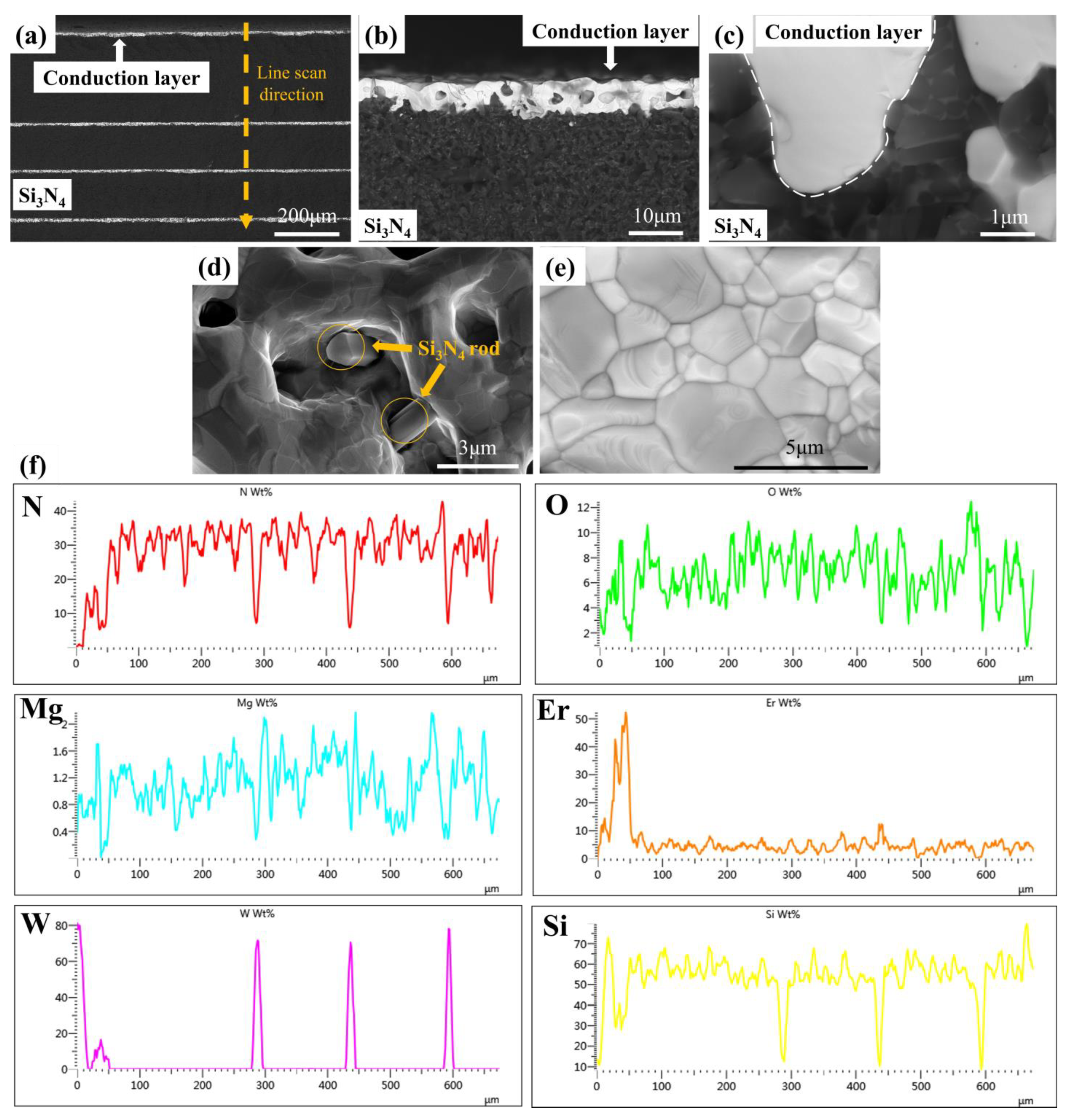
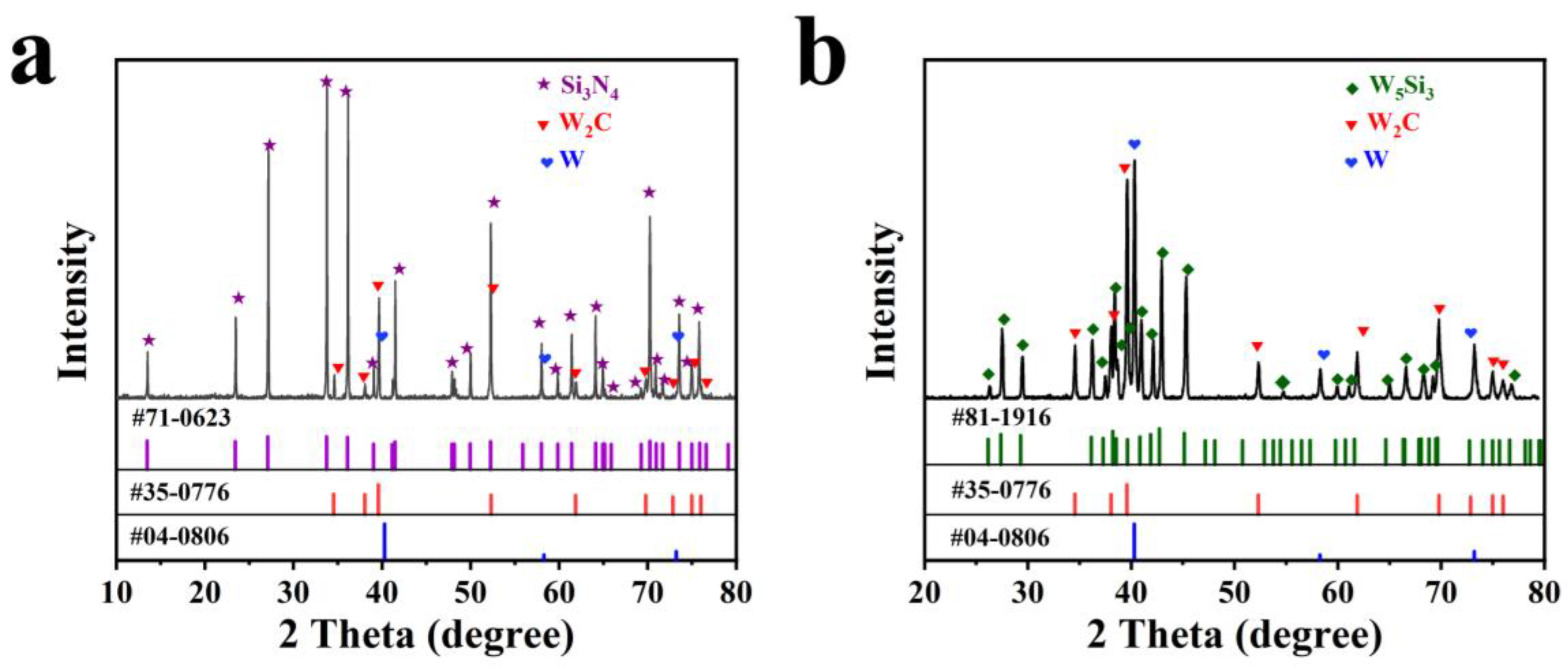
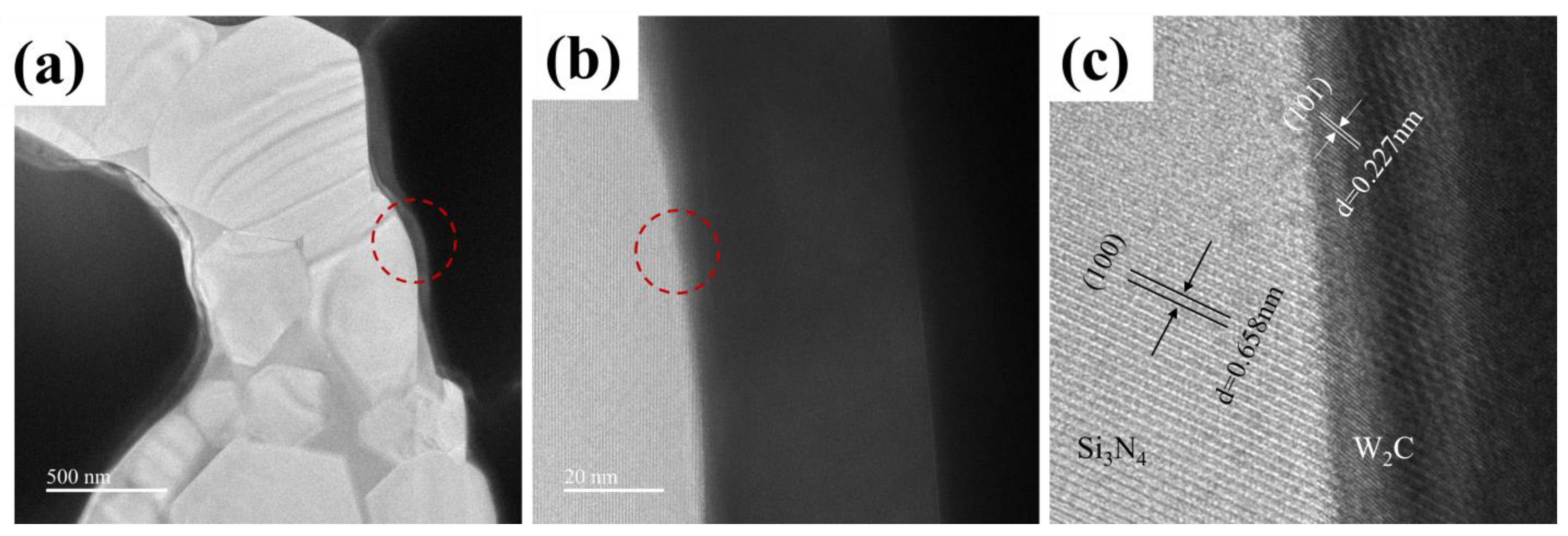
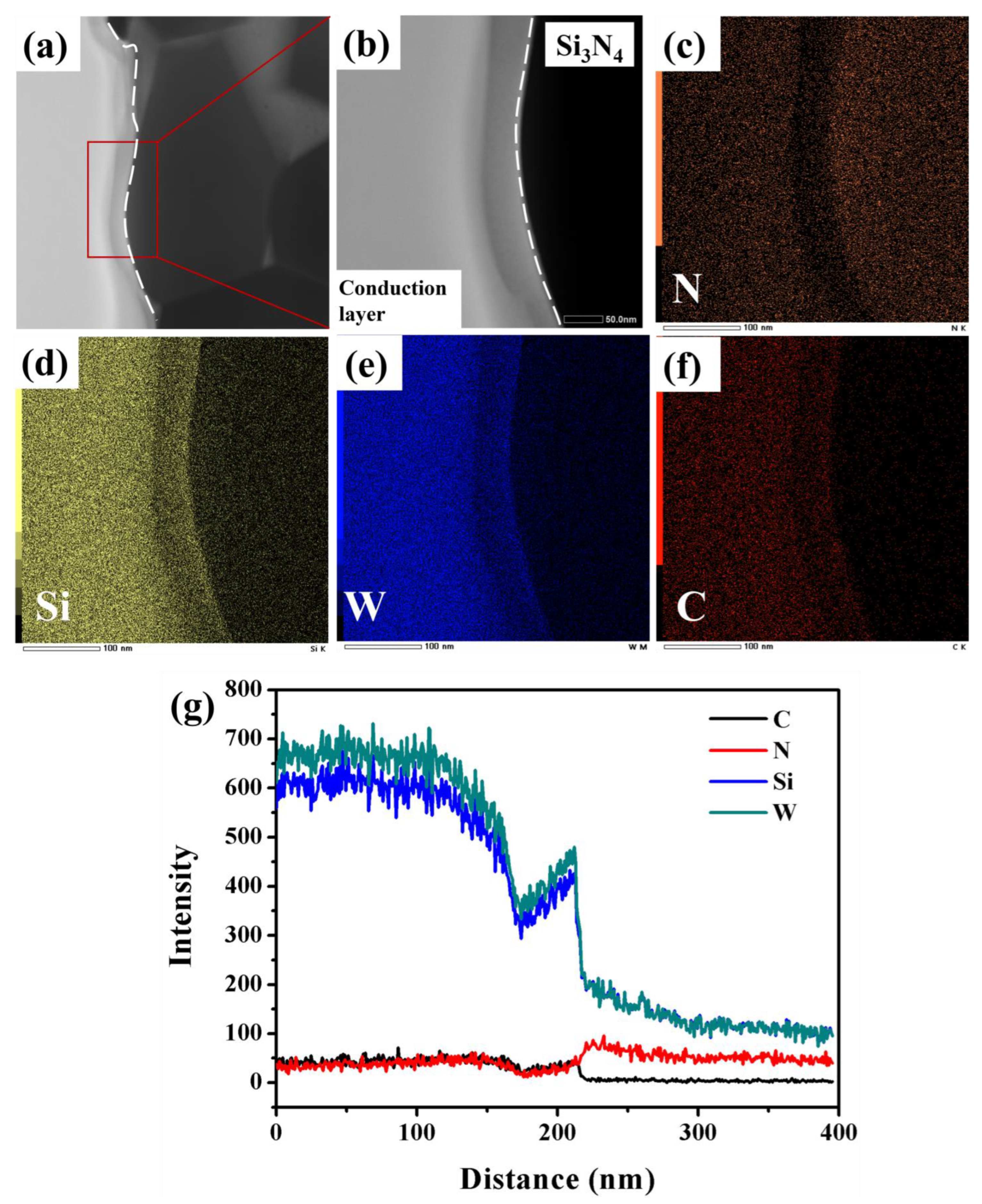
3.3. Discussion of Interfacial Bonding between Si3N4 Substrate and Conduction Layer

To investigate the microstructure and composition of the Si3N4 HTCC, Figure 4 presents the XRD test of the polished cross section and the conduction layer surface for sample 3#. As shown in Figure 4a, the main phase composition of the Si3N4 HTCC was Si3N4, W2C and W. This supports the view that W reacted with residual carbon after debinding. Figure 4b shows the XRD test of the conduction layer surface, indicating that the crystal phases of the metal layer mainly consisted of W2C, W and W5Si3. To further explore the combination mechanism between the Si3N4 ceramic and conduction layer, TEM and HRTEM analyses were performed. Figure 5a depicts a Si3N4 rod penetrating deeply into the conduction layer, thus verifying the physical model of the mechanical interlocking structure. Figure 5b displays the distinct white and gray zones with a clear interface. Figure 5c is a high-resolution image of the selected area in Figure 5b. Two distinct lattice fringes are visible, representing the crystal plane spacing of 0.658 nm of Si3N4 (100) (PDF: 71-0623) and 0.227 nm of W2C (101) (PDF: 35-0776).
Figure 6a–g illustrate the EDS analysis results in order to further understand the composition of the interface. EDS mapping clearly shows the distribution of the N, Si, W and C elements in Figure 6c–f, respectively. The change in the energy spectrum of the elements indicates that diffusion occurred during the co-firing process. Prior to co-firing, W was present in the conduction layer, while Si and N were present in Si3N4. After co-firing, a significant accumulation of Si and N elements was observed on the side of the conduction layer, while the concentration of the W element was lower on the Si3N4 side. This suggests that the diffusion of N and Si elements to the conduction layer was more pronounced during the co-firing process, while the diffusion of the W element to the Si3N4 side was relatively weak. Observation of Figure 6g reveals that the degree of aggregation of Si and W elements was relatively consistent with the change in their concentrations. It is clear that Si, W and C elements were enriched in the conduction layer and decreased toward the Si3N4 substrate. The N element was primarily present in the Si3N4 substrate and secondarily in the conduction layer. The intermediate platform observed in the EDS mapping was a sample stage due to the difference in thickness from the sample preparation process using focused ion beam (FIB) milling. According to the XRD test, it was determined that the chemical species of W and C in the conduction layer was the W2C phase. This indicates that the degree of variation in the concentration of W and C elements is consistent. As Figure 6a indicates, Si3N4 grains can be clearly observed. Consequently, Si and N elements exist primarily in the form of Si3N4. However, as it approached the conduction layer, the N element decreased while the Si element increased. Thus, on the conduction layer side, the primary form of the Si element is not Si3N4 but W5Si3. According to previous reports and Figure 4b, W reacts with Si3N4 during sintering as follows [34]:
5W + Si3N4 = W5Si3 + 2N2 (g) ΔG = −155.62 kJ/mol (1830 °C)
Therefore, Si and W elements accumulate only at the interface to form the W5Si3 compound. The main reason for the accumulation of Si and W on the conduction layer side of the interface could be that the diffusion rate of Si and N atoms was much faster than that of W atoms during co-firing. W5Si3 is a strong covalent compound, and excessive W5Si3 would weaken the conductivity of the conduction layer. Moreover, the presence of W2C acted as a diffusion barrier for Si3N4 ceramic [35], which inhibited the interfacial reaction and was beneficial to the conductivity of the conduction layer. According to the line scanning of Si and W elements obtained in Figure 3f, it could be found that the aggregation degree of the Si element dropped sharply as it gradually approached the center of the conduction layer, and the W element appeared to do the opposite. Therefore, it can be inferred that the formation of W5Si3 was an interfacial reaction, and the degree of reaction decreased rapidly when approaching the middle of the conduction layer. To sum up, the schematic illustration of the preparation of Si3N4 HTCC and the interfacial bonding mechanism is shown in Figure 7. W2C and W5Si3 coexisted at the interface to provide great reactive wetting. W5Si3 accumulated at the interface of the conduction layer side and decreased towards the Si3N4 side and the center of the conduction layer.

4. Conclusions

In this study, Si3N4 HTCC with W paste as the conducting layer was prepared successfully through tape-casting of Si green tape, screen-printing of the W conduction layer and a high-temperature co-firing method. Si3N4 HTCC with high interfacial bonding (5.25 kgf/mm2) and good square resistance (98.8 ± 20 mΩ/sq) can be developed with the addition of Si3N4 powder.
It was found that the addition of Si3N4 to the W paste showed an obvious influence on the interfacial bonding. Adding Si3N4 powder is beneficial to the thermal expansion coefficient matching between the Si3N4 ceramic and the conduction layer, which leads to less thermal stress and better dissolution-driven wetting.
The interfacial bonding of the Si3N4 ceramic and the conduction layer was discussed in detail. W combined with residual carbon to form W2C and reacted with Si3N4 to produce W5Si3, which provided reactive wetting for the interface, and the presence of W2C weakened the formation of W5Si3, which made a balance between great adhesion strength and conductivity for Si3N4 HTCC. This work provides guidance for promoting the application of the Si3N4 ceramic in the electronics device field, with a view for it to be an alternate HTCC substrate for AlN in industrial applications.

Author Contributions

Conceptualization, L.-F.W. and J.-X.Z.; methodology, L.-F.W. and N.L.; software, L.-F.W., B.-A.Z. and Z.L.; validation, L.-F.W. and Y.-S.D.; formal analysis, L.-F.W.; investigation, L.-F.W.; resources, L.-F.W.; data curation, L.-F.W.; writing—original draft preparation, L.-F.W.; writing—review and editing, L.-F.W. and J.-X.Z.; visualization, L.-F.W.; supervision, J.-X.Z. and Y.-S.D.; project administration, J.-X.Z. and Y.-S.D.; funding acquisition, J.-X.Z. and Y.-S.D. All authors have read and agreed to the published version of the manuscript.

Funding

This research was funded by the National Key Research and Development Program of China, grant number 2022YFB3706300, National Natural Science Foundation of China, grant number N52102082, Shanghai Science and Technology Committee, grant number 21YF1454500.

Institutional Review Board Statement

Not applicable.

Informed Consent Statement

Not applicable.

Data Availability Statement

All the data is available within the manuscript.

Acknowledgments

This work was supported by the State Key Laboratory of High Performance Ceramics and Superfine Microstructure of Shanghai Institute Ceramics, Chinese Academy of Sciences.

Conflicts of Interest

The authors declare no conflict of interest. The authors declare that they have no known competing financial interests or personal relationships that could have appeared to influence the work reported in this paper.

References

  1. Sešek, A.; Makarovič, K. Metallization, Material Selection, and Bonding of Interconnections for Novel LTCC and HTCC Power Modules. Materials 2022, 15, 1036. [Google Scholar] [CrossRef] [PubMed]
  2. Scognamillo, C.; Catalano, A.; Riccio, M.; D’Alessandro, V.; Codecasa, L.; Borghese, A.; Tripathi, R.; Castellazzi, A.; Breglio, G.; Irace, A. Compact Modeling of a 3.3 kV SiC MOSFET Power Module for Detailed Circuit-Level Electrothermal Simulations Including Parasitics. Energies 2021, 14, 4683. [Google Scholar] [CrossRef]
  3. Wu, B.; Chen, R.; Fu, R.; Agathopoulos, S.; Su, X.; Liu, H. Low thermal expansion coefficient and high thermal conductivity epoxy/Al2O3/T-ZnOw composites with dual-scale interpenetrating network structure. Compos. Part A Appl. Sci. Manuf. 2020, 137, 105993. [Google Scholar] [CrossRef]
  4. Garman, P.D.; Johnson, J.M.; Talesara, V.; Yang, H.; Zhang, D.; Castro, J.; Lu, W.; Hwang, J.; Lee, L.J. Silicon Oxycarbide Accelerated Chemical Vapor Deposition of Graphitic Networks on Ceramic Substrates for Thermal Management Enhancement. ACS Appl. Nano Mater. 2019, 2, 452–458. [Google Scholar] [CrossRef]
  5. Feng, X.; Lv, Y.; Zhang, L.; Ge, D.; Li, X.; Sun, J.; Ding, J.; Chen, L.; Zheng, K.; Zhang, X.; et al. Effect of AlN addition on phase formation in the LTCC with Al2O3/AlN biphasic ceramics based on BBSZ glass. Ceram. Int. 2020, 46, 16895–16900. [Google Scholar] [CrossRef]
  6. Wang, Y.; Xu, Y.-H.; Cao, Z.-Y.; Yan, C.; Wang, K.; Chen, J.-J.; Cheng, S.-Y.; Feng, Z.-S. A facile process to manufacture high performance copper layer on ceramic material via biomimetic modification and electroless plating. Compos. Part B Eng. 2018, 157, 123–130. [Google Scholar] [CrossRef]
  7. Kaneko, T.; Watanabe, H. AlN HTCC super miniaturized millimeterwave transceiver MCMs, the novel structure for the high reliability, the high performance and the mass productivity. In Proceedings of the 1999 IEEE MTT-S International Microwave Symposium Digest (Cat. No. 99CH36282), Anaheim, CA, USA, 13–19 June 1999; Volume 442, pp. 449–452. [Google Scholar]
  8. Menzel, W.; Kassner, J. Millimeter-Wave 3D Integration Techniques using LTCC and Related Multilayer Circuits. In Proceedings of the 2000 30th European Microwave Conference, Paris, France, 2–5 October 2000; pp. 1–4. [Google Scholar]
  9. Mizoe, J.; Amano, S. Miniature 60 GHz transmitter/receiver modules on AlN multi-layer high temperature co-fired ceramic. In Proceedings of the 1999 IEEE MTT-S International Microwave Symposium Digest (Cat. No. 99CH36282), Anaheim, CA, USA, 13–19 June 1999; Volume 472, pp. 475–478. [Google Scholar]
  10. Chen, Y.; Hou, X.; Fang, Z.; Wang, E.; Chen, J.; Bei, G. Adsorption and Reaction of Water on the AlN(0001) Surface from First Principles. J. Phys. Chem. C 2019, 123, 5460–5468. [Google Scholar] [CrossRef]
  11. Park, H.; Kim, H.-E.; Niihara, K. Microstructural Evolution and Mechanical Properties of Si3N4 with Yb2 O3 as a Sintering Additive. J. Am. Ceram. Soc. 1997, 80, 750–756. [Google Scholar] [CrossRef]
  12. Kleebe, H.-J.; Pezzotti, G.; Ziegler, G. Microstructure and Fracture Toughness of Si3N4 Ceramics: Combined Roles of Grain Morphology and Secondary Phase Chemistry. J. Am. Ceram. Soc. 1999, 82, 1857–1867. [Google Scholar] [CrossRef]
  13. Yoon, K.J.; Wiederhorn, S.M.; Luecke, W.E. Comparison of Tensile and Compressive Creep Behavior in Silicon Nitride. J. Am. Ceram. Soc. 2000, 83, 2017–2022. [Google Scholar] [CrossRef]
  14. Li, J.-Q.; Luo, F.; Zhu, D.-M.; Zhou, W.-C. Influence of Phase Formation on Dielectric Properties of Si3N4 Ceramics. J. Am. Ceram. Soc. 2007, 90, 1950–1952. [Google Scholar] [CrossRef]
  15. Xiang, H.; Feng, Z.; Li, Z.; Zhou, Y. Theoretical predicted high-thermal-conductivity cubic Si3N4 and Ge3N4: Promising substrate materials for high-power electronic devices. Sci. Rep. 2018, 8, 14374. [Google Scholar] [CrossRef] [Green Version]
  16. Hu, F.; Xie, Z.-P.; Zhang, J.; Hu, Z.-L.; An, D. Promising high-thermal-conductivity substrate material for high-power electronic device: Silicon nitride ceramics. Rare Met. 2020, 39, 463–478. [Google Scholar] [CrossRef]
  17. Yin, X.; Kong, L.; Zhang, L.; Cheng, L.; Travitzky, N.; Greil, P. Electromagnetic properties of Si–C–N based ceramics and composites. Int. Mater. Rev. 2014, 59, 326–355. [Google Scholar] [CrossRef]
  18. Hirao, K.; Zhou, Y.; Hyuga, H.; Ohji, T.; Kusano, D. High Thermal Conductivity Silicon Nitride Ceramics. J. Korean Ceram. Soc. 2012, 49, 380–384. [Google Scholar] [CrossRef]
  19. Zhou, Y.; Hyuga, H.; Kusano, D.; Yoshizawa, Y.-I.; Hirao, K. A Tough Silicon Nitride Ceramic with High Thermal Conductivity. Adv. Mater. 2011, 23, 4563–4567. [Google Scholar] [CrossRef]
  20. Trehan, V.; Trickey, S.; Indacochea, J.; Lugscheider, E.; Buschke, I.; Tillmann, W. Brazing of Silicon Nitride with Reactive Filler Metals. Sci. Eng. Compos. Mater. 1999, 8, 107–112. [Google Scholar] [CrossRef]
  21. He, J.-G.; Dai, S.-J.; Zhao, Y.; Huang, M.; Liu, Y.; Yu, J.-Q.; Tan, Y.; Fan, L.-W.; Ge, W.-Q.; Ma, Y.-F. Improvements in Brazed-Joint Properties of Silicon Nitride and Titanium Alloys Using Laser-Induced Microscale Rice Leaf Structures. Materials 2022, 15, 6750. [Google Scholar] [CrossRef]
  22. Reed, L.; Huggins, R.A. Electron Probe Microanalysis of Ceramic-to-Metal Seals. J. Am. Ceram. Soc. 1965, 48, 421–426. [Google Scholar] [CrossRef]
  23. Fulrath, R.; Hollar, E. Manganese Glass-Molybdenum Metallizing Ceramics. Am. Ceram. Soc. Bull. 1968, 47, 493. [Google Scholar]
  24. Twentyman, M.E.; Popper, P. High-temperature metallizing. J. Mater. Sci. 1975, 10, 777–790. [Google Scholar] [CrossRef]
  25. Cui, S.; Huang, A. Study on Cofired Multiplayer AlN Substrates for MCMs. Electron. Compon. Mater. 2003, 22, 25–28. [Google Scholar] [CrossRef]
  26. Hu, Y.; Jiang, M. The Influence of SiO2 Concentration in the Tungsten Paste for AlN Cofire Multi-layer Ceramic Substrate. Mater. Rep. 2004, 18, 88–90. [Google Scholar]
  27. de Faoite, D.; Browne, D.J.; Chang-Díaz, F.R.; Stanton, K.T. A review of the processing, composition, and temperature-dependent mechanical and thermal properties of dielectric technical ceramics. J. Mater. Sci. 2012, 47, 4211–4235. [Google Scholar] [CrossRef] [Green Version]
  28. Knibbs, R.H. The measurement of thermal expansion coefficient of tungsten at elevated temperatures. J. Phys. E Sci. Instrum. 1969, 2, 515–517. [Google Scholar] [CrossRef]
  29. Nagy, D.; Humphry-Baker, S.A. An oxidation mechanism map for tungsten. Scr. Mater. 2022, 209, 114373. [Google Scholar] [CrossRef]
  30. Son, S.; Park, K.; Katoh, Y.; Kohyama, A. Interfacial reactions and mechanical properties of W–SiC in-situ joints for plasma facing components. J. Nucl. Mater. 2004, 329–333, 1549–1552. [Google Scholar] [CrossRef]
  31. Choe, J.; Calat, J.N.; Lu, G.-Q. Constrained-film sintering of a gold circuit paste. J. Mater. Res. 1995, 10, 986–994. [Google Scholar] [CrossRef]
  32. Jansson, S.; Leckie, F. Reduction of Thermal Stresses in Continuous Fiber Reinforced Metal Matrix Composites with Interface Layers. J. Compos. Mater. 1992, 26, 1474–1486. [Google Scholar] [CrossRef]
  33. Singler, T.J.; Su, S.; Yin, L.; Murray, B.T. Modeling and experiments in dissolutive wetting: A review. J. Mater. Sci. 2012, 47, 8261–8274. [Google Scholar] [CrossRef]
  34. Wang, L.; Qi, Q.; Zhang, H.; Yang, X.; Liu, Z.; Wu, H.; Liu, X.; Huang, Z. The fabrication of tungsten reinforced silicon nitride ceramics by altering nitrogen pressure. Ceram. Int. 2019, 45, 5927–5931. [Google Scholar] [CrossRef]
  35. Mustain, H.A.; Brown, W.D.; Ang, S.S. Tungsten Carbide as a Diffusion Barrier on Silicon Nitride Active- Metal-Brazed Substrates for Silicon Carbide Power Devices. J. Electron. Packag. 2009, 131, 034502. [Google Scholar] [CrossRef]
Figure 1. Thermal analysis of green multilayer in nitrogen/air atmosphere and W powder in air.
Materials 16 02937 g001
Figure 2. SEM micrographs of the conduction band surface in different stages. (a,b) Green tape, (d,e) after debinding, (g,h) after nitriding with (c,f,i) corresponding XRD pattern.
Materials 16 02937 g002
Figure 3. SEM micrographs of Si3N4 HTCC cross section (a) ×120 (b) ×2000 (c) ×20,000. SEM micrographs of (d) exposed Si3N4 rods in conduction layer (e) and its grains after sintering. (f) N, O, Mg, Er, W and Si elements’ linear scanning curves of the direction in (a).
Materials 16 02937 g003
Figure 4. XRD pattern of 3# Si3N4 HTCC. (a) Cross section of Si3N4 HTCC. (b) The surface of conduction layer.
Materials 16 02937 g004
Figure 5. TEM images (a) of Si3N4 grain embedding in conduction layer, (b) profile of the interface between Si3N4 grain and conduction layer pointed by the circle in (a,c) HRTEM image of the interface pointed by the circle in (b).
Materials 16 02937 g005
Figure 6. (a) Bright-field (BF) image of the interface and (b) the local amplification graph for EDS mapping and its corresponding (c) N mapping, (d) Si mapping, (e) W mapping, (f) C mapping and (g) its line scanning curves.
Materials 16 02937 g006
Figure 7. Schematic illustration of the preparation of Si3N4 HTCC and interfacial bonding mechanism.
Materials 16 02937 g007
Table 1. The effect of Si3N4 additive on W film resistance and adhesion strength.
ω(Si3N4)/(vol%)W Film Resistance/(mΩ/sq)Adhesion Strength/(kgf/mm2)Thermal Expansion Coefficient/(10−6/K)
1#0110.72.834.5
2#8.7192.083.104.20
3#17.4298.755.253.91
4#27.23146.47.043.57
Disclaimer/Publisher’s Note: The statements, opinions and data contained in all publications are solely those of the individual author(s) and contributor(s) and not of MDPI and/or the editor(s). MDPI and/or the editor(s) disclaim responsibility for any injury to people or property resulting from any ideas, methods, instructions or products referred to in the content.

