
Semiconductor Characterization by Terahertz Excitation Spectroscopy

Abstract
:1. Introduction
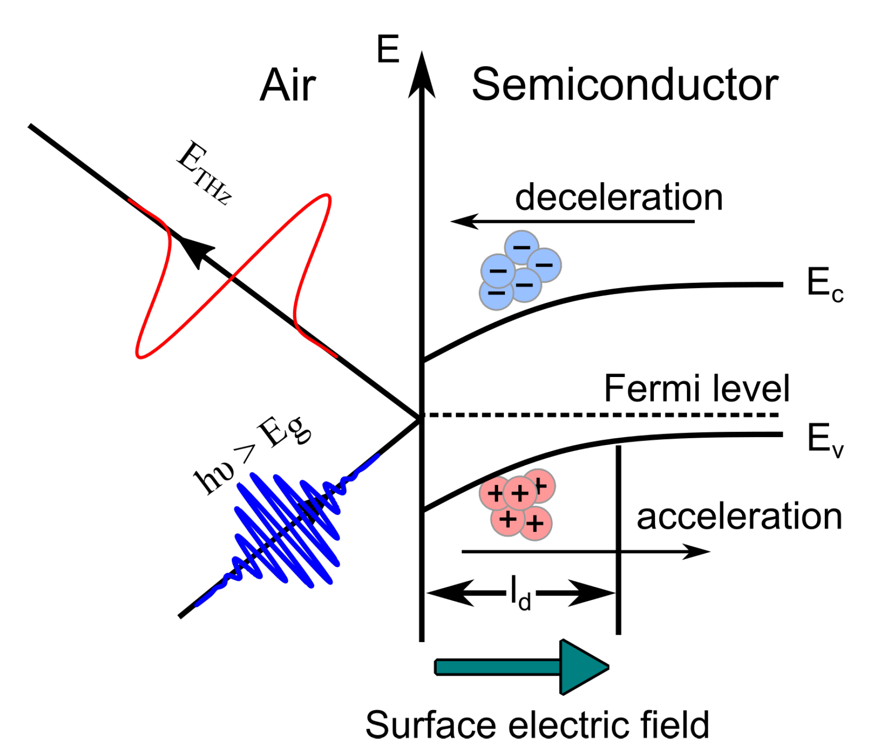
2. Mechanisms of Surface THz Emission
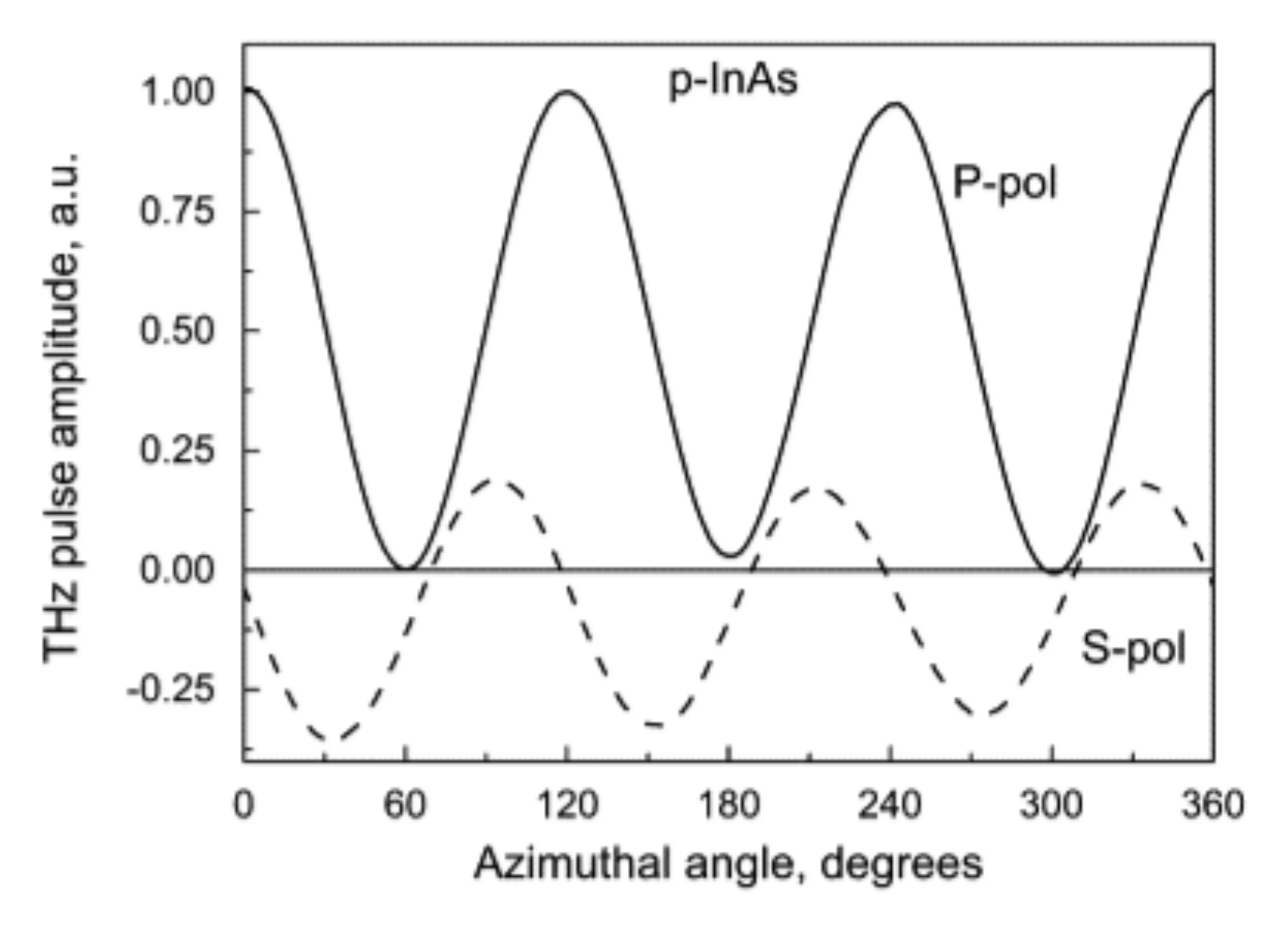
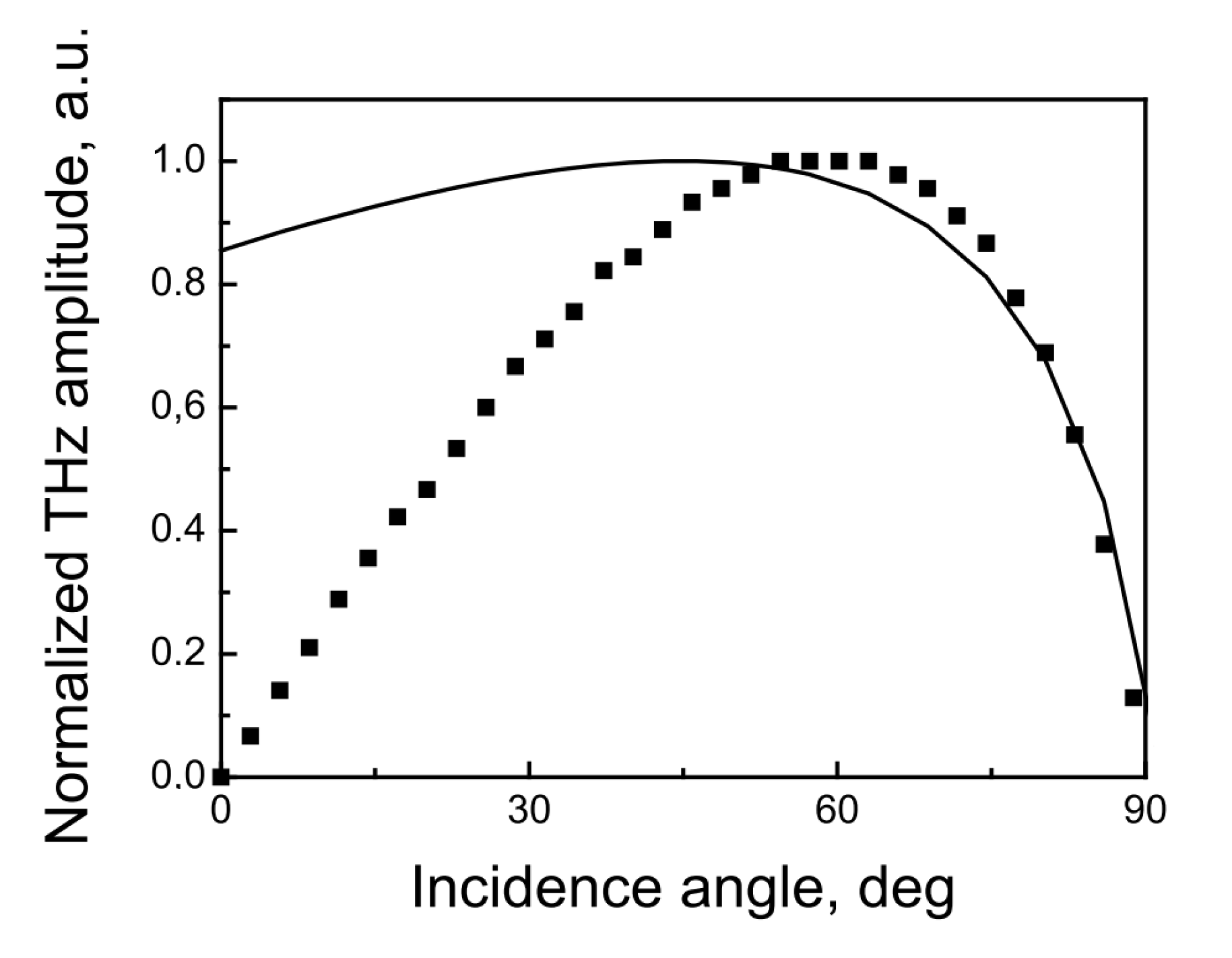
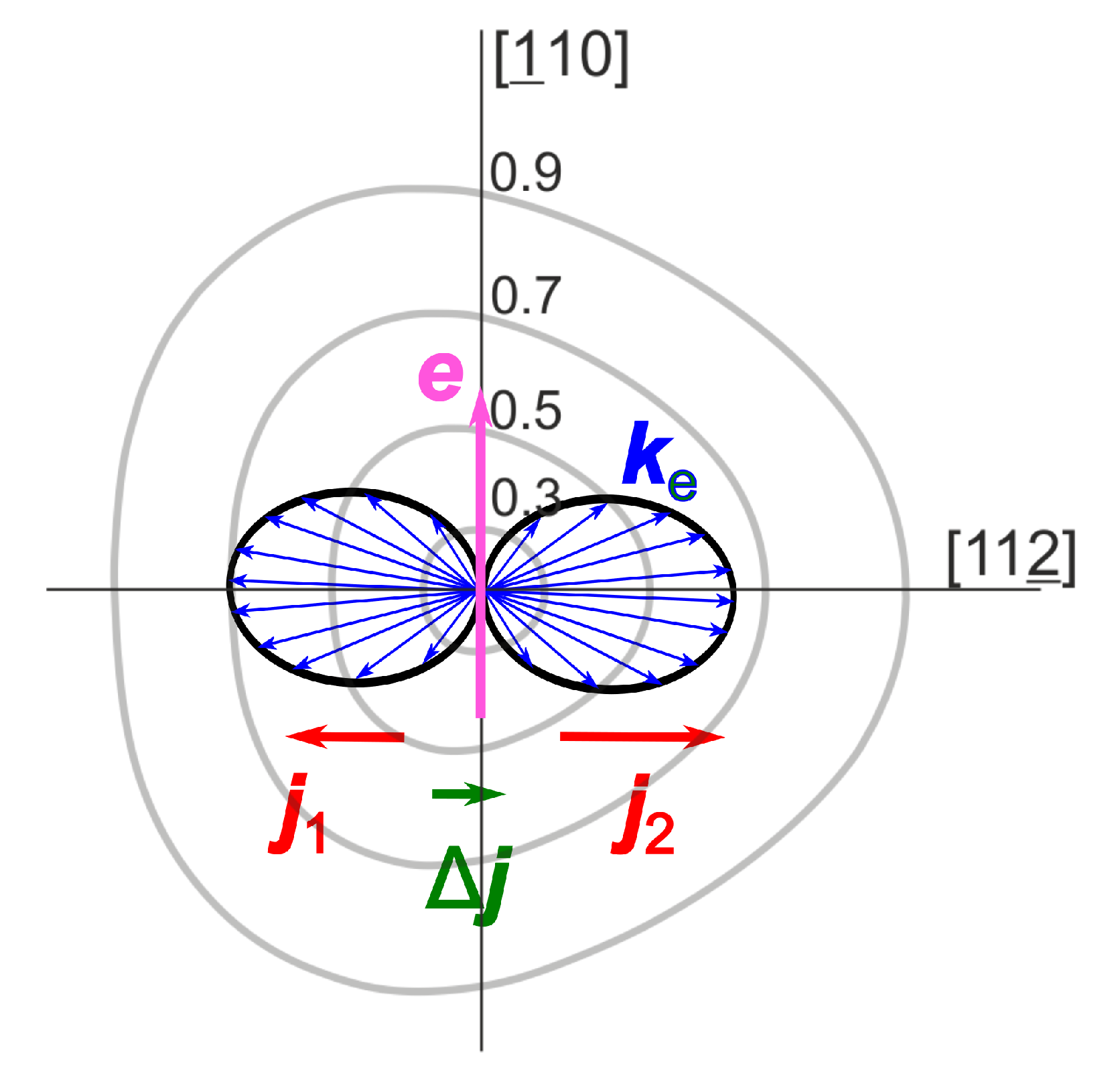
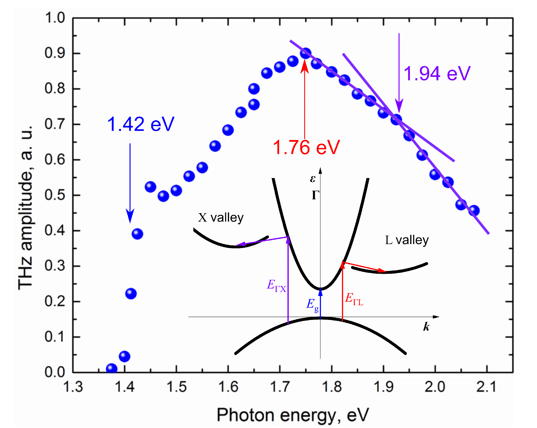
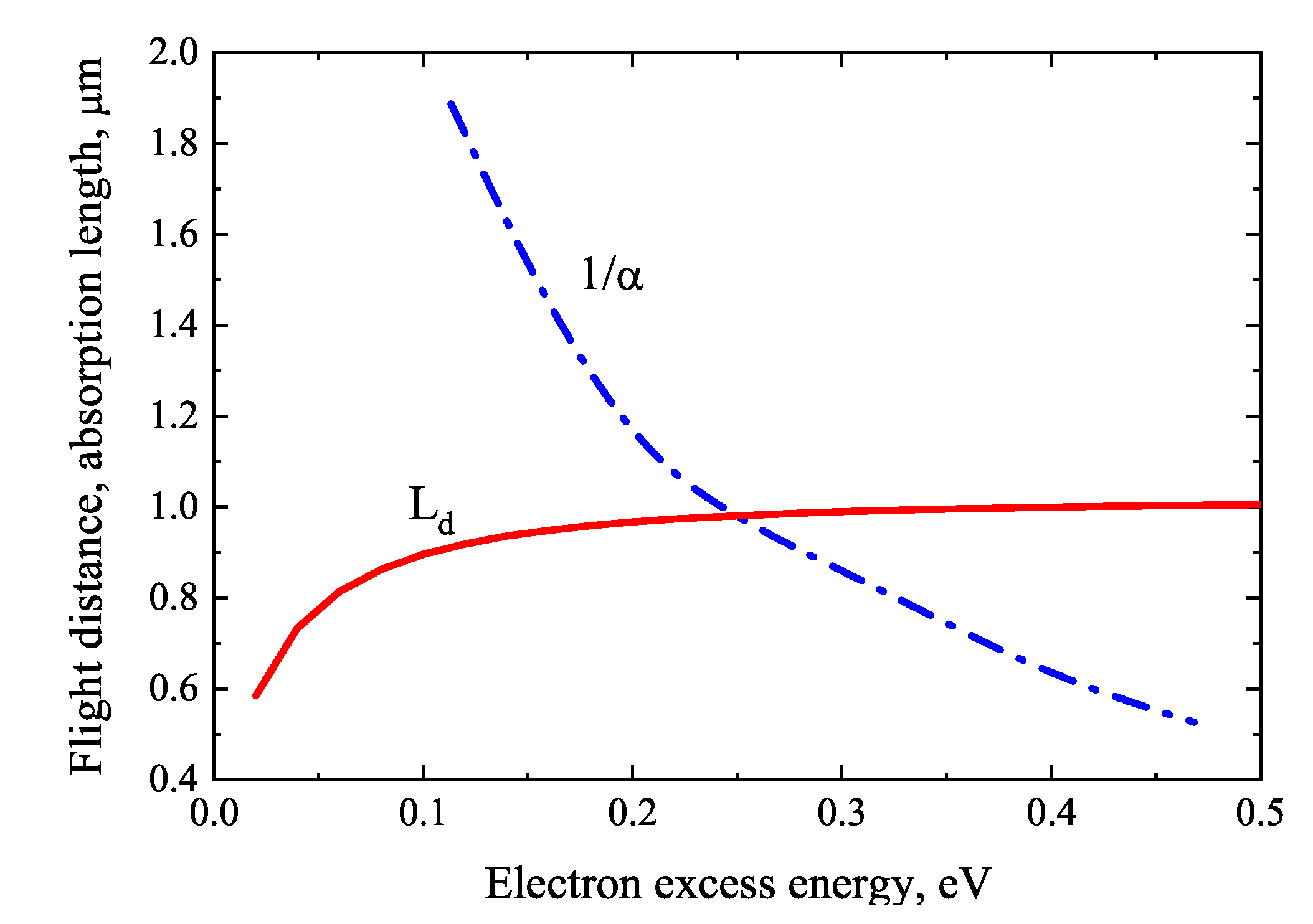
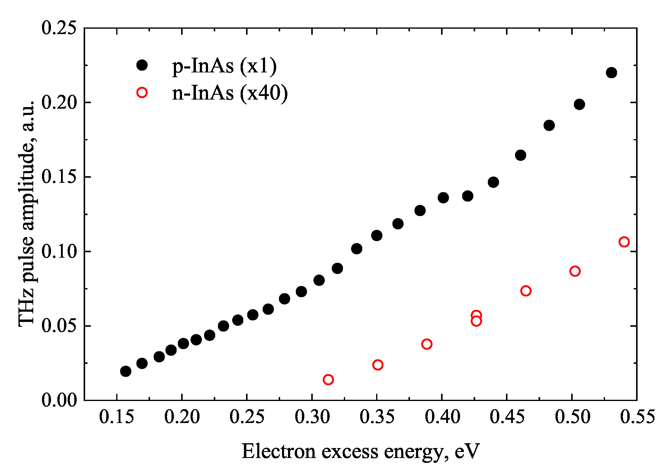
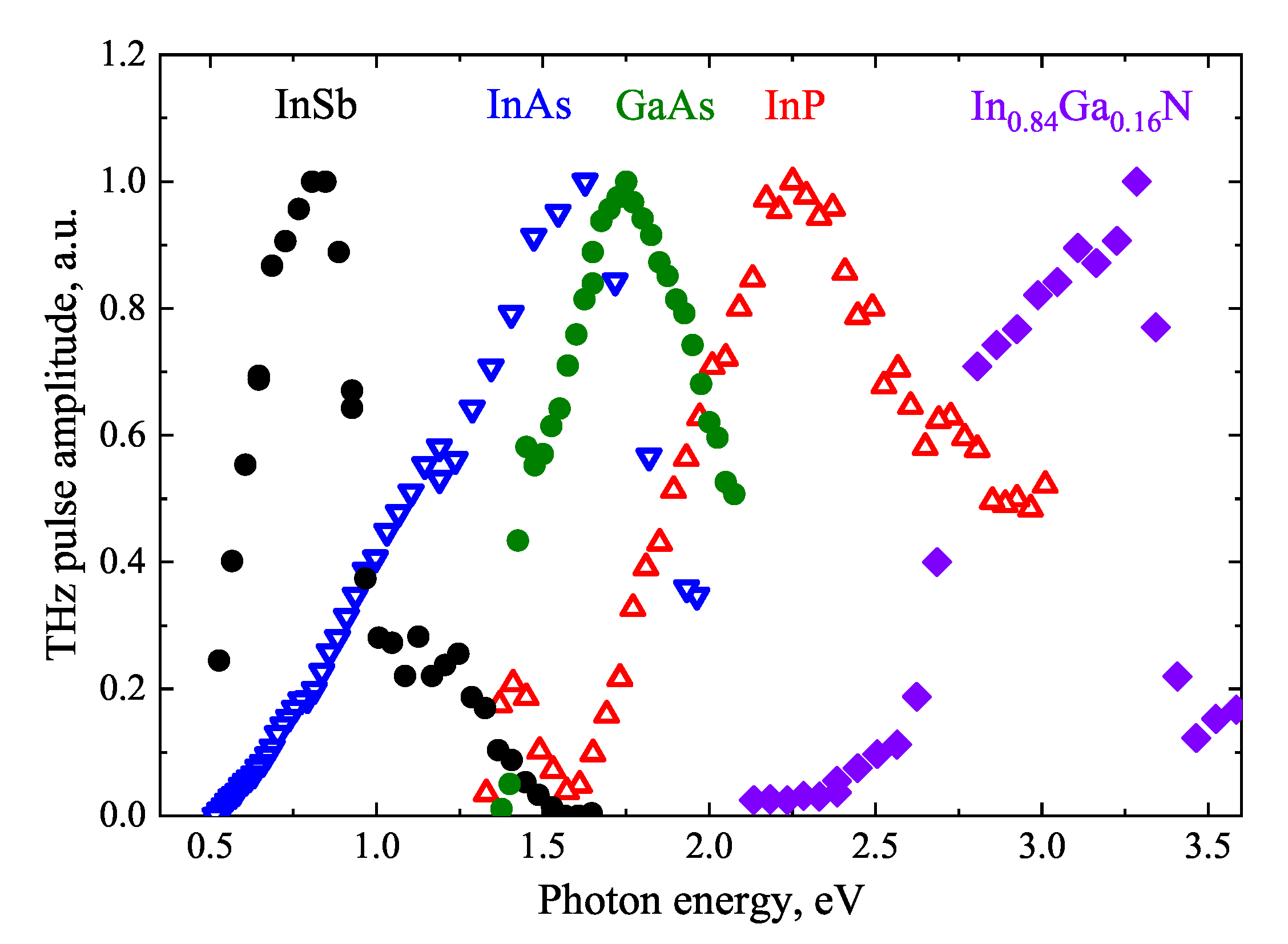
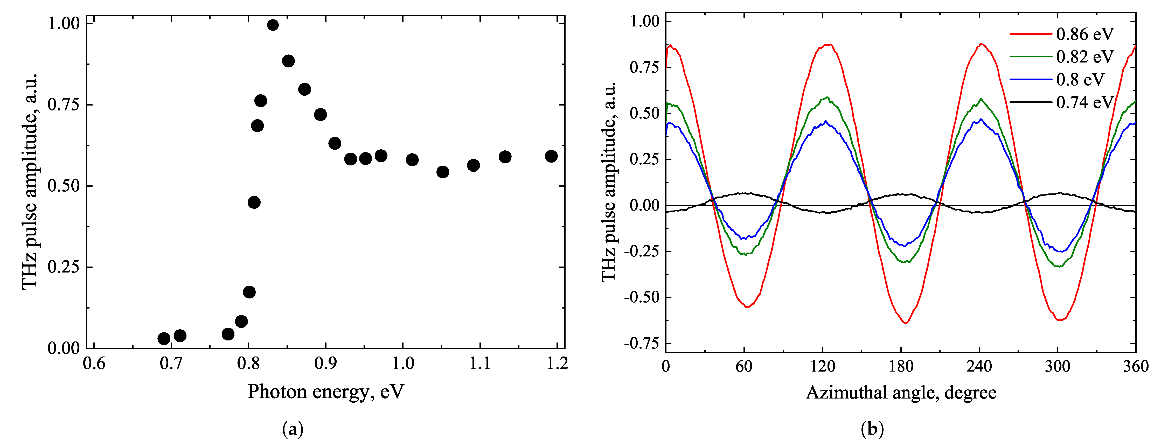
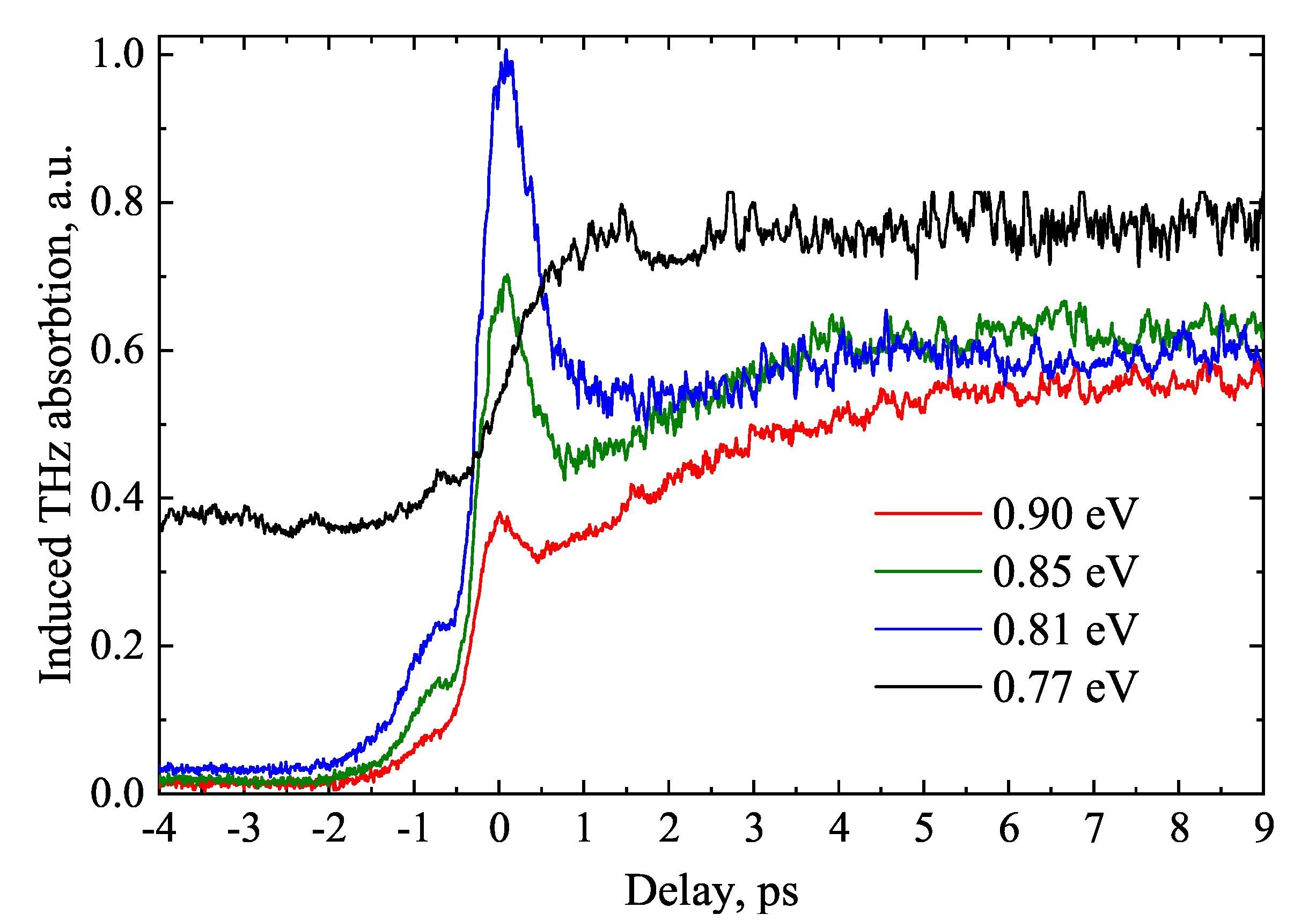
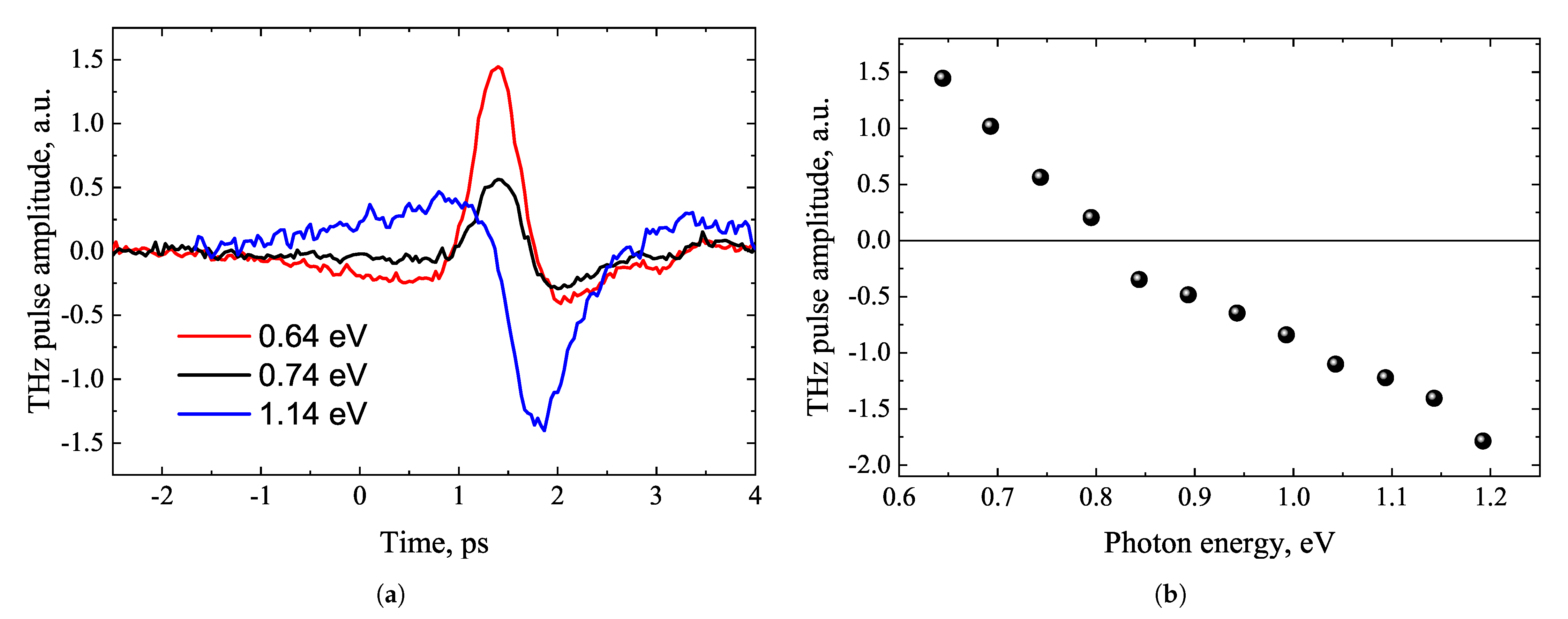
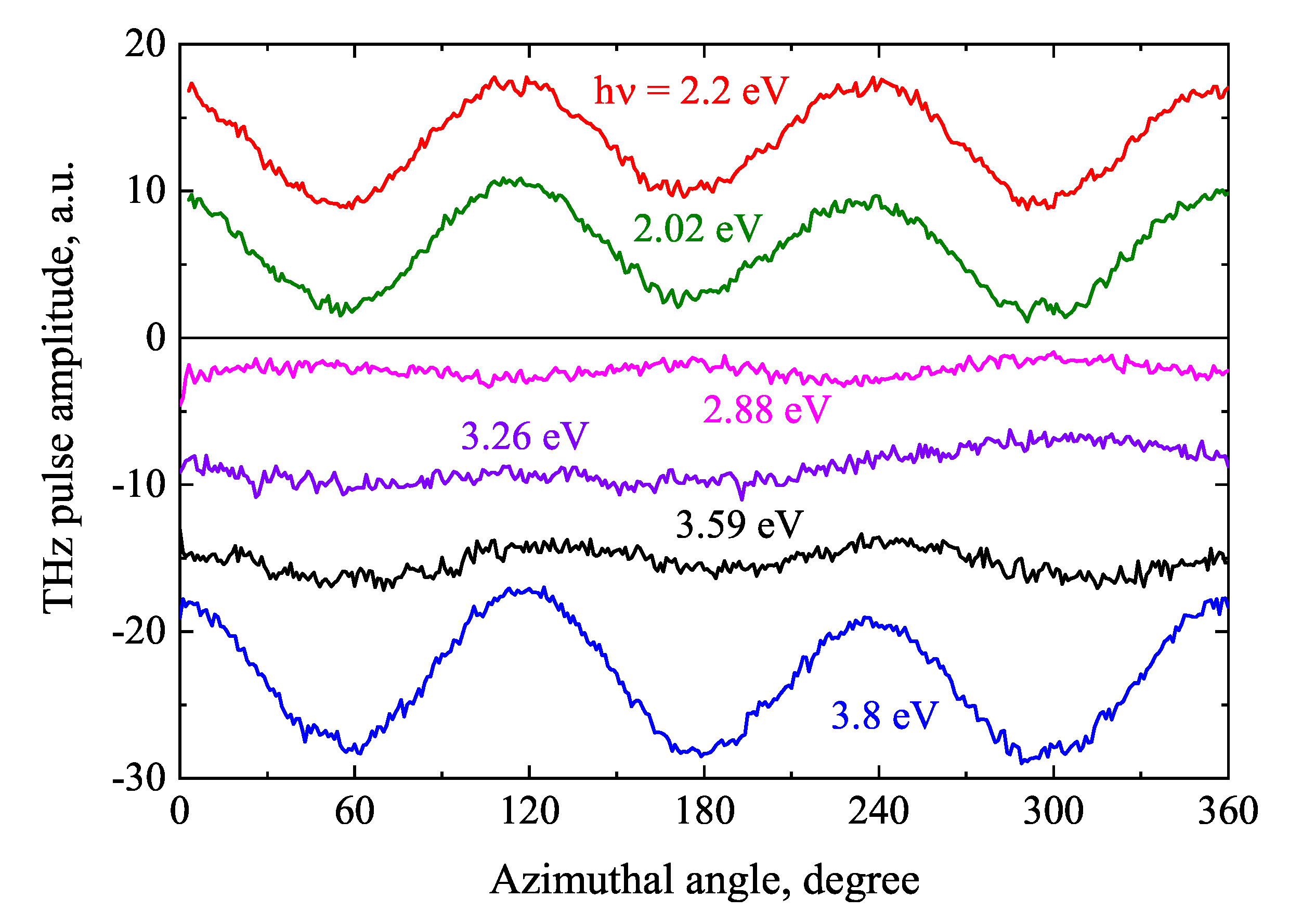
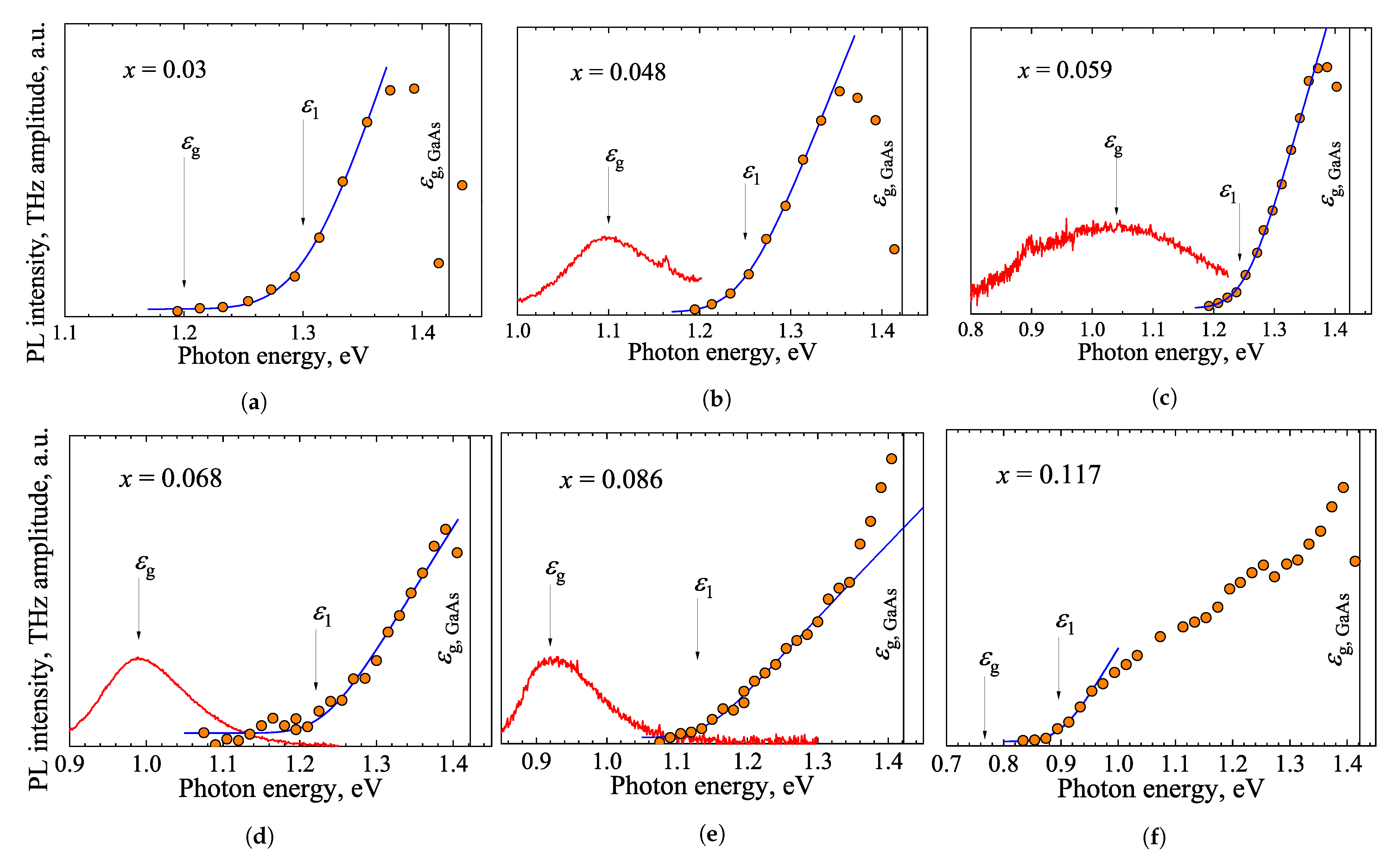
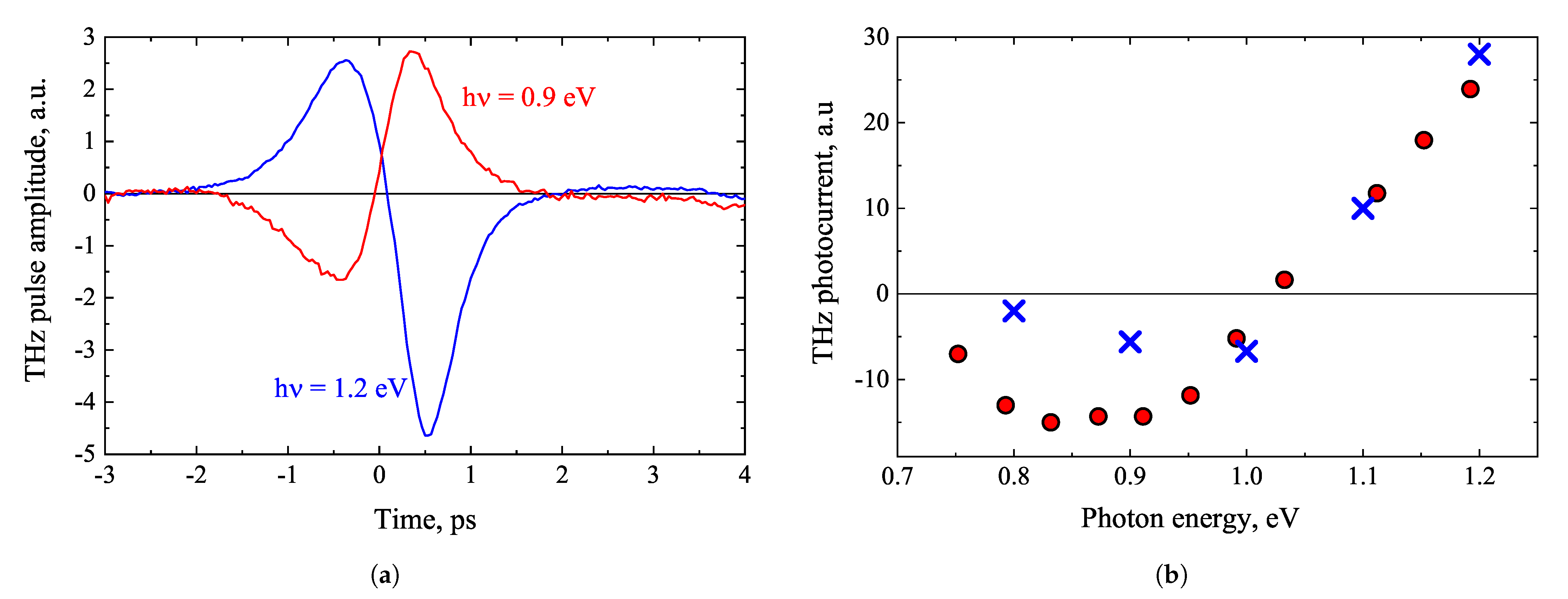
3. THz Excitation Spectroscopy of A3B5 Semiconductors
4. Other Semiconductor Crystals
4.1. Germanium
4.2. Tellurium
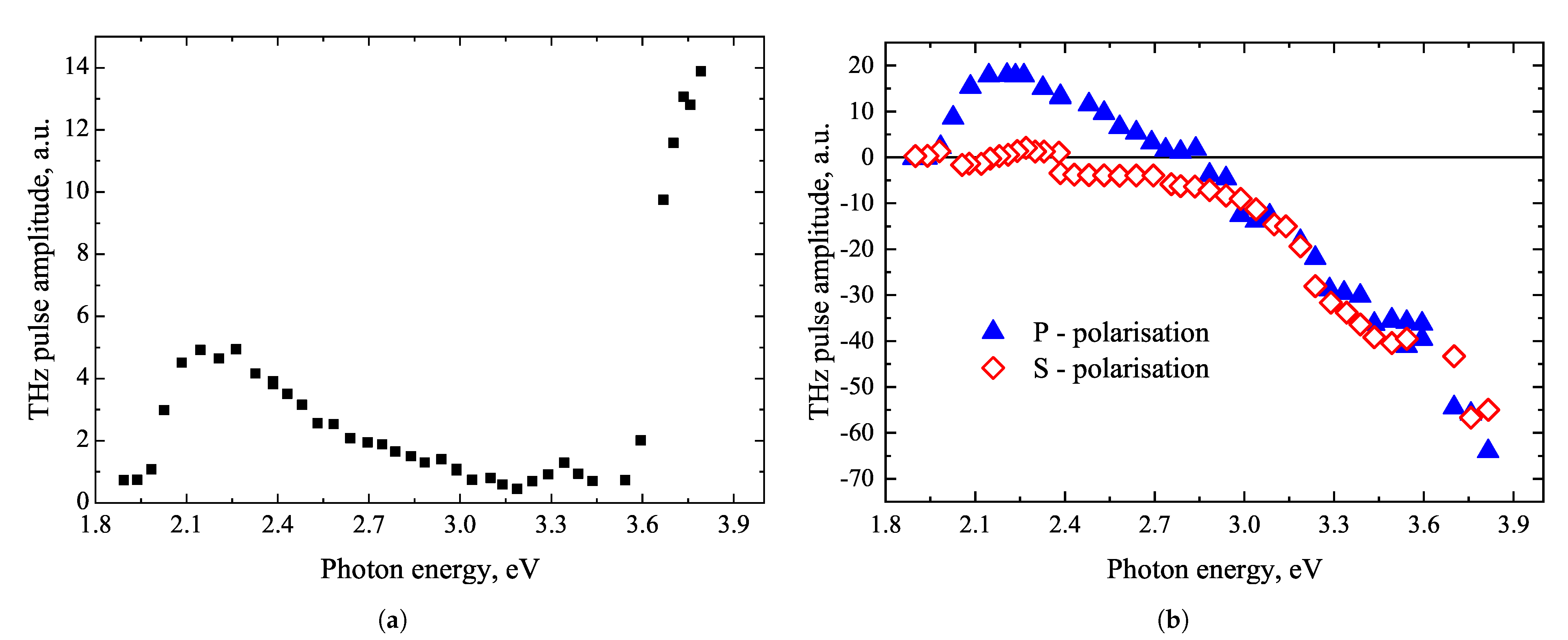
4.3. Gallium Selenide
5. Semiconductor Nanostructures
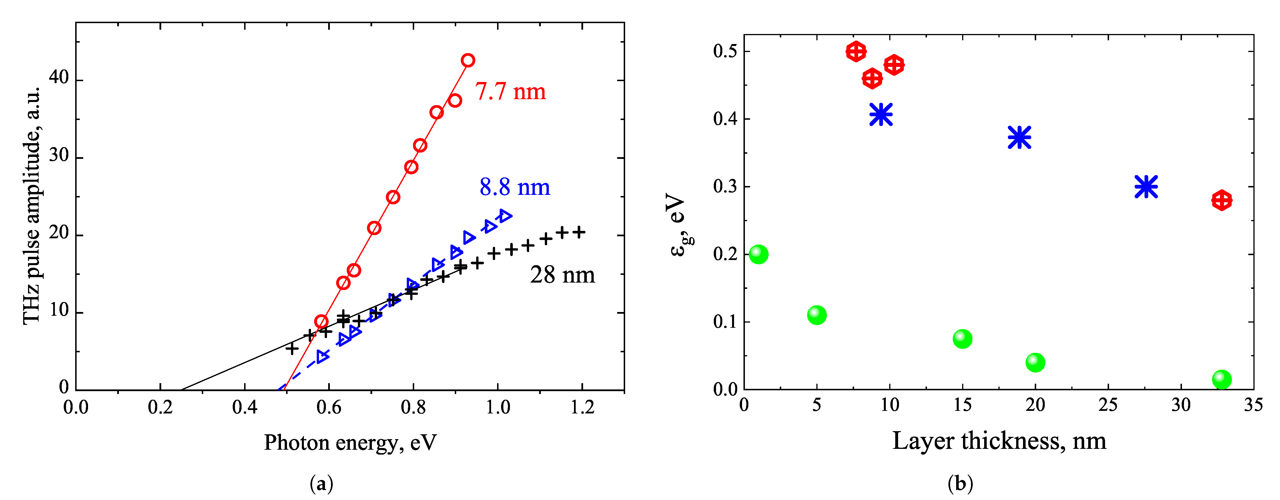
5.1. Bismuth Layers
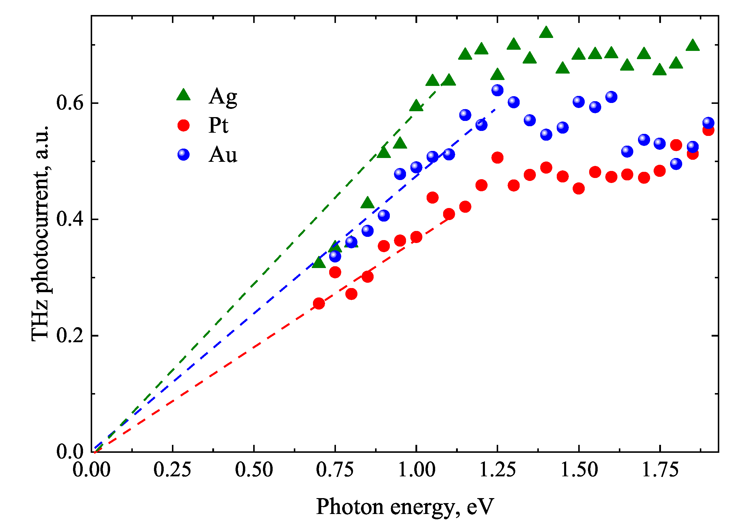
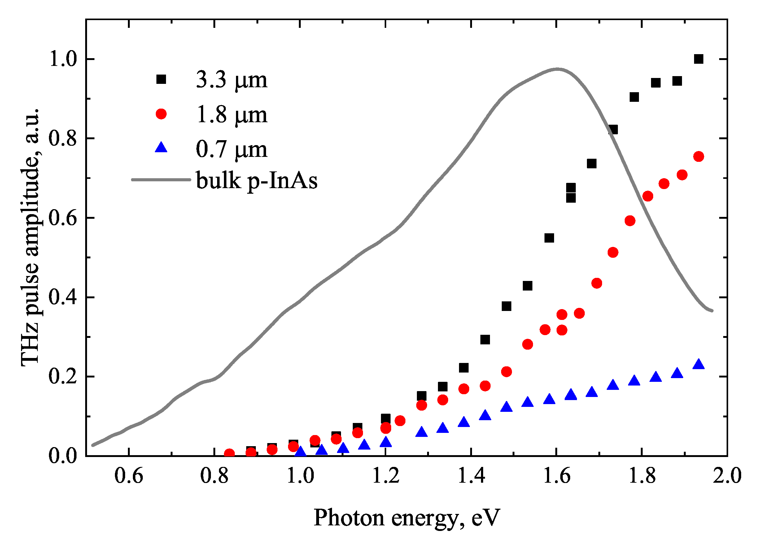
5.2. InAs Nanowires
6. Heterostructure Band Offsets
7. Conclusions and Insights for the Future
Author Contributions
Funding
Data Availability Statement
Conflicts of Interest
Abbreviations
| TES | Terahertz Excitation Spectroscopy |
References
- Auston, D.H.; Cheung, K.P.; Smith, P.R. Picosecond Photoconducting Hertzian Dipoles. Appl. Phys. Lett. 1984, 45, 284–286. [Google Scholar] [CrossRef]
- Grischkowsky, D.; Keiding, S.; van Exter, M.; Fattinger, C. Far-Infrared Time-Domain Spectroscopy with Terahertz Beams of Dielectrics and Semiconductors. J. Opt. Soc. Am. B 1990, 7, 2006. [Google Scholar] [CrossRef]
- Kadlec, F.; Kužel, P.; Coutaz, J.L. Optical Rectification at Metal Surfaces. Opt. Lett. 2004, 29, 2674. [Google Scholar] [CrossRef] [PubMed]
- Chen, Y.; Yamaguchi, M.; Wang, M.; Zhang, X.C. Terahertz Pulse Generation from Noble Gases. Appl. Phys. Lett. 2007, 91, 251116. [Google Scholar] [CrossRef]
- Jin, Q.; E, Y.; Williams, K.; Dai, J.; Zhang, X.C. Observation of Broadband Terahertz Wave Generation from Liquid Water. Appl. Phys. Lett. 2017, 111, 071103. [Google Scholar] [CrossRef]
- Zhang, X.C.; Hu, B.B.; Darrow, J.T.; Auston, D.H. Generation of Femtosecond Electromagnetic Pulses from Semiconductor Surfaces. Appl. Phys. Lett. 1990, 56, 1011–1013. [Google Scholar] [CrossRef]
- Zhang, X.C.; Auston, D.H. Optoelectronic Measurement of Semiconductor Surfaces and Interfaces with Femtosecond Optics. J. Appl. Phys. 1992, 71, 326–338. [Google Scholar] [CrossRef]
- Adomavičius, R.; Molis, G.; Krotkus, A.; Sirutkaitis, V. Spectral Dependencies of Terahertz Emission from InAs and InSb. Appl. Phys. Lett. 2005, 87, 261101. [Google Scholar] [CrossRef]
- Karpus, V.; Norkus, R.; Butkutė, R.; Stanionytė, S.; Čechavičius, B.; Krotkus, A. THz-excitation Spectroscopy Technique for Band-Offset Determination. Opt. Express 2018, 26, 33807. [Google Scholar] [CrossRef]
- Bičiūnas, A.; Pačebutas, V.; Krotkus, A. Terahertz Pulse Emission from Semiconductor Surfaces Illuminated by Femtosecond Yb:KGW Laser Pulses. Phys. B Condens. Matter 2009, 404, 3386–3390. [Google Scholar] [CrossRef]
- Adomavičius, R.; Urbanowicz, A.; Molis, G.; Krotkus, A.; Šatkovskis, E. Terahertz Emission from P-lnAs Due to the Instantaneous Polarization. Appl. Phys. Lett. 2004, 85, 2463–2465. [Google Scholar] [CrossRef]
- Krotkus, A. Semiconductors for terahertz photonics applications. J. Phys. D: Appl. Phys. 2010, 43, 273001. [Google Scholar] [CrossRef] [Green Version]
- Dekorsy, T.; Auer, H.; Bakker, H.J.; Roskos, H.G.; Kurz, H. THz Electromagnetic Emission by Coherent Infrared-Active Phonons. Phys. Rev. B 1996, 53, 4005–4014. [Google Scholar] [CrossRef] [PubMed] [Green Version]
- Chuang, S.L.; Schmitt-Rink, S.; Greene, B.I.; Saeta, P.N.; Levi, A.F.J. Optical Rectification at Semiconductor Surfaces. Phys. Rev. Lett. 1992, 68, 102–105. [Google Scholar] [CrossRef] [PubMed] [Green Version]
- Reid, M.; Cravetchi, I.V.; Fedosejevs, R. Terahertz Radiation and Second-Harmonic Generation from InAs: Bulk versus Surface Electric-Field-Induced Contributions. Phys. Rev. B 2005, 72, 035201. [Google Scholar] [CrossRef] [Green Version]
- Tonouchi, M. Simplified Formulas for the Generation of Terahertz Waves from Semiconductor Surfaces Excited with a Femtosecond Laser. J. Appl. Phys. 2020, 127, 245703. [Google Scholar] [CrossRef]
- Malevich, V.L.; Ziaziulia, P.A.; Adomavičius, R.; Krotkus, A.; Malevich, Y.V. Terahertz Emission from Cubic Semiconductor Induced by a Transient Anisotropic Photocurrent. J. Appl. Phys. 2012, 112, 073115. [Google Scholar] [CrossRef]
- Shank, C.V.; Zakharchenya, B.P. Spectroscopy of Nonequilibrium Electrons and Phonons; Elsevier Science: Amsterdam, The Netherlands, 2014. [Google Scholar]
- Zakharchenya, B.P.; Mirlin, D.N.; Perel’, V.I.; Reshina, I.I. Spectrum and Polarization of Hot-Electron Photoluminescence in Semiconductors. Sov. Phys. Uspekhi 1982, 25, 143–166. [Google Scholar] [CrossRef]
- Belinicher, V.I.; Novikov, V.N. Sov. Physics. Semicond. 1981, 15, 1138. [Google Scholar]
- Cicėnas, P.; Geižutis, A.; Malevich, V.L.; Krotkus, A. Terahertz Radiation from an InAs Surface Due to Lateral Photocurrent Transients. Opt. Lett. 2015, 40, 5164. [Google Scholar] [CrossRef]
- Nevinskas, I.; Vizbaras, K.; Trinkūnas, A.; Butkutė, R.; Krotkus, A. Terahertz Pulse Generation from (111)-Cut InSb and InAs Crystals When Illuminated by 155-Mm Femtosecond Laser Pulses. Opt. Lett. 2017, 42, 2615. [Google Scholar] [CrossRef]
- Arlauskas, A.; Krotkus, A. THz Excitation Spectra of AIIIBV Semiconductors. Semicond. Sci. Technol. 2012, 27, 115015. [Google Scholar] [CrossRef]
- Reklaitis, A. Crossover between Surface Field and Photo-Dember Effect Induced Terahertz Emission. J. Appl. Phys. 2011, 109, 083108. [Google Scholar] [CrossRef]
- Hackenberg, W.; Fasol, G. Polar Optic Phonon and Γ→ L Intervalley Scatt. Times GaAs Steady-State Hot-Electron Lumin. Spectrosc. Appl. Phys. Lett. 1990, 57, 174–176. [Google Scholar] [CrossRef]
- Su, F.H.; Blanchard, F.; Sharma, G.; Razzari, L.; Ayesheshim, A.; Cocker, T.L.; Titova, L.V.; Ozaki, T.; Kieffer, J.C.; Morandotti, R.; et al. Terahertz Pulse Induced Intervalley Scattering in Photoexcited GaAs. Opt. Express 2009, 17, 9620. [Google Scholar] [CrossRef]
- Nag, B.R. Electron Transport in Compound Semiconductors; Number 11 in Springer Series in Solid-State Sciences; Springer: Berlin/Heidelberg, Germany, 1980. [Google Scholar]
- InSb Band Structure. Available online: http://www.ioffe.ru/SVA/NSM/Semicond/InSb/bandstr.html (accessed on 3 March 2023).
- Willardson, R.K.; Beer, A.C. Optical Properties of III–V Compounds; Academic Press: New York, NY, USA, 1967. [Google Scholar]
- Norkus, R.; Aleksiejūnas, R.; Kadys, A.; Kolenda, M.; Tamulaitis, G.; Krotkus, A. Spectral dependence of THz emission from InN and InGaN layers. Sci. Rep. 2019, 9, 7077. [Google Scholar] [CrossRef] [PubMed] [Green Version]
- Arlauskas, A.; Subačius, L.; Krotkus, A.; Malevich, V.L. Terahertz emission from InSb illuminated by femtosecond laser pulses. J. Phys. D Appl. Phys. 2017, 50, 055101. [Google Scholar] [CrossRef]
- Nevinskas, I.; Butkutė, R.; Stanionytė, S.; Bičiūnas, A.; Geižutis, A.; Krotkus, A. THz pulse emission from InAs-based epitaxial structures grown on InP substrates. Semicond. Sci. Technol. 2016, 31, 115021. [Google Scholar] [CrossRef]
- Nevinskas, I.; Kadlec, F.; Kadlec, C.; Butkutė, R.; Krotkus, A. Terahertz pulse emission from epitaxial n-InAs in a magnetic field. J. Phys. D Appl. Phys. 2019, 52, 365301. [Google Scholar] [CrossRef]
- Norkus, R.; Arlauskas, A.; Krotkus, A. Terahertz excitation spectra of InP single crystals. Semicond. Sci. Technol. 2018, 33, 075010. [Google Scholar] [CrossRef]
- Nevinskas, I.; Vizbaras, K.; Vizbaras, A.; Trinkūnas, A.; Krotkus, A. Magnetic field enhanced terahertz pulse emission from a femtosecond laser excited GaSb epitaxial layer. Electron. Lett. 2016, 52, 1627–1629. [Google Scholar] [CrossRef]
- Nevinskas, I.; Stanionytė, S.; Pačebutas, V.; Krotkus, A. Terahertz emission from GaInAs P-i-ndiodes Photoexcited Femtosecond Laser Pulses. Lith. J. Phys. 2016, 55. [Google Scholar] [CrossRef] [Green Version]
- Pačebutas, V.; Stanionytė, S.; Arlauskas, A.; Norkus, R.; Butkutė, R.; Geižutis, A.; Čechavičius, B.; Krotkus, A. Terahertz Excitation Spectra of GaAsBi Alloys. J. Phys. D Appl. Phys. 2018, 51, 474001. [Google Scholar] [CrossRef]
- Germanium. Available online: www.ioffe.ru/SVA/NSM/Semicond/Ge/ (accessed on 3 March 2023).
- Norkus, R.; Nevinskas, I.; Krotkus, A. Spectral Dependencies of Terahertz Emission from Femtosecond Laser Excited Surfaces of Germanium Crystals. J. Appl. Phys. 2019, 126, 225704. [Google Scholar] [CrossRef]
- Urbanowicz, A.; Krotkus, A.; Adomavičius, R.; Malevich, V. Terahertz Emission from Femtosecond Laser Excited Ge Surfaces Due to the Electrical Field-Induced Optical Rectification. Phys. B: Condens. Matter 2007, 398, 98–101. [Google Scholar] [CrossRef]
- Bičiūnas, A.; Arlauskas, A.; Adamonis, J.; Cicėnas, P.; Krotkus, A. Physical Mechanisms of Terahertz Pulse Emission from Photoexcited Surfaces of Tellurium Crystals. J. Appl. Phys. 2014, 116, 093102. [Google Scholar] [CrossRef]
- Genzow, D. Transverse Dember Effect and Anisotropy of Carrier Mobilities in Tellurium Single Crystals. Phys. Status Solidi (b) 1973, 55, 547–557. [Google Scholar] [CrossRef]
- Ribakovs, G.; Gundjian, A.A. Theory of the Photon Drag Effect in Tellurium. J. Appl. Phys. 1977, 48, 4609–4612. [Google Scholar] [CrossRef]
- Ivchenko, E.L.; Pikus, G.E. New photogalvanic effect in gyrotropic crystals. JETP Lett. 1976, 27, 604. [Google Scholar]
- Peng, H.; Kioussis, N.; Snyder, G.J. Elemental Tellurium as a Chiral p -Type Thermoelectric Material. Phys. Rev. B 2014, 89, 195206. [Google Scholar] [CrossRef] [Green Version]
- Link, R. Zur anomalen Vorzeichenumkehr des Hallkoeffizienten in Tellur. Phys. Status Solidi (b) 1965, 12, 81–92. [Google Scholar] [CrossRef]
- Asauskas, R.; Balynas, V.; Dobrovolskis, Z.; Krotkus, A.; Hoerstel, W. Electron transfer effect in intrinsic tellurium single crystals. J. Phys. Colloq. 1981, 42, C7–329–C7–334. [Google Scholar] [CrossRef] [Green Version]
- Yang, D.Q.; Zhu, L.Q.; Wang, J.L.; Xia, W.; Zhang, J.Z.; Jiang, K.; Shang, L.Y.; Li, Y.W.; Hu, Z.G. Band Structure and Lattice Vibration of Elemental Tellurium Investigated by Temperature-Dependent Mid-and-Far Infrared Transmission and Raman Spectroscopy. Phys. Status Solidi (b) 2022, 259, 2100625. [Google Scholar] [CrossRef]
- Hegenbarth, R.; Steinmann, A.; Sarkisov, S.; Giessen, H. Milliwatt-Level Mid-Infrared (105–165 Mm) Difference Frequency Generation with a Femtosecond Dual-Signal-Wavelength Optical Parametric Oscillator. Opt. Lett. 2012, 37, 3513. [Google Scholar] [CrossRef]
- Shi, W.; Ding, Y.J.; Fernelius, N.; Vodopyanov, K. Efficient, Tunable, and Coherent 018–527-THz Source Based on GaSe Crystal. Opt. Lett. 2002, 27, 1454. [Google Scholar] [CrossRef] [Green Version]
- Liu, K.; Xu, J.; Zhang, X.C. GaSe Crystals for Broadband Terahertz Wave Detection. Appl. Phys. Lett. 2004, 85, 863–865. [Google Scholar] [CrossRef]
- Keilmann, F.; Gohle, C.; Holzwarth, R. Time-Domain Mid-Infrared Frequency-Comb Spectrometer. Opt. Lett. 2004, 29, 1542. [Google Scholar] [CrossRef] [Green Version]
- Huber, R.; Brodschelm, A.; Tauser, F.; Leitenstorfer, A. Generation and Field-Resolved Detection of Femtosecond Electromagnetic Pulses Tunable up to 41 THz. Appl. Phys. Lett. 2000, 76, 3191–3193. [Google Scholar] [CrossRef]
- Sporken, R.; Hafsi, R.; Coletti, F.; Debever, J.M.; Thiry, P.A.; Chevy, A. Inverse-Photoemission Spectroscopy of GaSe and InSe. Phys. Rev. B 1994, 49, 11093–11099. [Google Scholar] [CrossRef]
- Schwarz, U.; Olguin, D.; Cantarero, A.; Hanfland, M.; Syassen, K. Effect of Pressure on the Structural Properties and Electronic Band Structure of GaSe. Phys. Status Solidi (b) 2007, 244, 244–255. [Google Scholar] [CrossRef]
- Norkus, R.; Nevinskas, I.; Krotkus, A. Terahertz Emission from a Bulk GaSe Crystal Excited by above Bandgap Photons. J. Appl. Phys. 2020, 128, 225701. [Google Scholar] [CrossRef]
- Zhai, D.; Herault, E.; Garet, F.; Coutaz, J.L.; Pan, C.L. THz Generation in GaSe Crystals Pumped with Laser Photon Energy below and around the Bandgap. Appl. Phys. Lett. 2023, 122, 011103. [Google Scholar] [CrossRef]
- Hartman, R. Temperature Dependence of the Low-Field Galvanomagnetic Coefficients of Bismuth. Phys. Rev. 1969, 181, 1070–1086. [Google Scholar] [CrossRef]
- Ogrin, Y.F.; Lutskii, V.N.; Elinson, M.I. Observation of Quantum Size Effects in Thin Bismuth Films. JETP Lett. 1966, 3, 114. [Google Scholar]
- Huber, T.E.; Nikolaeva, A.; Gitsu, D.; Konopko, L.; Foss, C.A.; Graf, M.J. Confinement Effects and Surface-Induced Charge Carriers in Bi Quantum Wires. Appl. Phys. Lett. 2004, 84, 1326–1328. [Google Scholar] [CrossRef] [Green Version]
- Chen, G.; Dresselhaus, M.S.; Dresselhaus, G.; Fleurial, J.P.; Caillat, T. Recent Developments in Thermoelectric Materials. Int. Mater. Rev. 2003, 48, 45–66. [Google Scholar] [CrossRef]
- Wang, Y.W.; Kim, J.S.; Kim, G.H.; Kim, K.S. Quantum Size Effects in the Volume Plasmon Excitation of Bismuth Nanoparticles Investigated by Electron Energy Loss Spectroscopy. Appl. Phys. Lett. 2006, 88, 143106. [Google Scholar] [CrossRef] [Green Version]
- Nevinskas, I.; Mockus, Z.; Juškėnas, R.; Norkus, R.; Selskis, A.; Norkus, E.; Krotkus, A. Terahertz Photoconductivity Spectra of Electrodeposited Thin Bi Films. Materials 2021, 14, 3150. [Google Scholar] [CrossRef]
- Devenson, J.; Norkus, R.; Juškėnas, R.; Krotkus, A. Terahertz Emission from Ultrathin Bismuth Layers. Opt. Lett. 2021, 46, 3681. [Google Scholar] [CrossRef]
- Faure, J.; Mauchain, J.; Papalazarou, E.; Marsi, M.; Boschetto, D.; Timrov, I.; Vast, N.; Ohtsubo, Y.; Arnaud, B.; Perfetti, L. Direct Observation of Electron Thermalization and Electron-Phonon Coupling in Photoexcited Bismuth. Phys. Rev. B 2013, 88, 075120. [Google Scholar] [CrossRef] [Green Version]
- Nevinskas, I.; Stanionytė, S.; Devenson, J.; Krotkus, A. Direct Bandgap Dependence of Bismuth Films on Their Thickness. J. Appl. Phys. 2022, 132, 055301. [Google Scholar] [CrossRef]
- Yang, Z.; Wu, Z.; Lyu, Y.; Hao, J. Centimeter-scale Growth of Two-dimensional Layered High-mobility Bismuth Films by Pulsed Laser Deposition. InfoMat 2019, 1, 98–107. [Google Scholar] [CrossRef] [Green Version]
- Hoffman, C.A.; Meyer, J.R.; Bartoli, F.J.; Di Venere, A.; Yi, X.J.; Hou, C.L.; Wang, H.C.; Ketterson, J.B.; Wong, G.K. Semimetal-to-Semiconductor Transition in Bismuth Thin Films. Phys. Rev. B 1993, 48, 11431–11434. [Google Scholar] [CrossRef]
- Milnes, A.; Polyakov, A. Indium Arsenide: A Semiconductor for High Speed and Electro-Optical Devices. Mater. Sci. Eng. B 1993, 18, 237–259. [Google Scholar] [CrossRef]
- Bolognesi, C.; Caine, E.; Kroemer, H. Improved Charge Control and Frequency Performance in InAs/AlSb-based Heterostructure Field-Effect Transistors. IEEE Electron Device Lett. 1994, 15, 16–18. [Google Scholar] [CrossRef]
- Paek, J.H.; Nishiwaki, T.; Yamaguchi, M.; Sawaki, N. Catalyst Free MBE-VLS Growth of GaAs Nanowires on (111)Si Substrate. Phys. Status Solidi C 2009, 6, 1436–1440. [Google Scholar] [CrossRef]
- Joyce, H.J.; Wong-Leung, J.; Yong, C.K.; Docherty, C.J.; Paiman, S.; Gao, Q.; Tan, H.H.; Jagadish, C.; Lloyd-Hughes, J.; Herz, L.M.; et al. Ultralow Surface Recombination Velocity in InP Nanowires Probed by Terahertz Spectroscopy. Nano Lett. 2012, 12, 5325–5330. [Google Scholar] [CrossRef] [PubMed] [Green Version]
- Joyce, H.J.; Parkinson, P.; Jiang, N.; Docherty, C.J.; Gao, Q.; Tan, H.H.; Jagadish, C.; Herz, L.M.; Johnston, M.B. Electron Mobilities Approaching Bulk Limits in “Surface-Free” GaAs Nanowires. Nano Lett. 2014, 14, 5989–5994. [Google Scholar] [CrossRef] [Green Version]
- Arlauskas, A.; Treu, J.; Saller, K.; Beleckaitė, I.; Koblmüller, G.; Krotkus, A. Strong Terahertz Emission and Its Origin from Catalyst-Free InAs Nanowire Arrays. Nano Lett. 2014, 14, 1508–1514. [Google Scholar] [CrossRef]
- Lin, A.; Shapiro, J.N.; Scofield, A.C.; Liang, B.L.; Huffaker, D.L. Enhanced InAs Nanopillar Electrical Transport by -Situ Passiv. Appl. Phys. Lett. 2013, 102, 053115. [Google Scholar] [CrossRef]
- Dayeh, S.A.; Yu, E.T.; Wang, D. Transport Coefficients of InAs Nanowires as a Function of Diameter. Small 2009, 5, 77–81. [Google Scholar] [CrossRef] [PubMed]
- Beleckaitė, I.; Treu, J.; Morkötter, S.; Döblinger, M.; Xu, X.; Adomavičius, R.; Finley, J.J.; Koblmüller, G.; Krotkus, A. Enhanced THz Emission Efficiency of Composition-Tunable InGaAs Nanowire Arrays. Appl. Phys. Lett. 2017, 110, 201106. [Google Scholar] [CrossRef]
- Robertson, J. Band Offsets, Schottky Barrier Heights, and Their Effects on Electronic Devices. J. Vac. Sci. Technol. A: Vacuum, Surfaces, Film. 2013, 31, 050821. [Google Scholar] [CrossRef]
- Broderick, C.A.; Usman, M.; Sweeney, S.J.; O’Reilly, E.P. Band Engineering in Dilute Nitride and Bismide Semiconductor Lasers. Semicond. Sci. Technol. 2012, 27, 094011. [Google Scholar] [CrossRef] [Green Version]
- Collar, K.; Li, J.; Jiao, W.; Guan, Y.; Losurdo, M.; Humlicek, J.; Brown, A.S. Determination of the Impact of Bi Content on the Valence Band Energy of GaAsBi Using X-Ray Photoelectron Spectroscopy. AIP Adv. 2017, 7, 075016. [Google Scholar] [CrossRef] [Green Version]
- Kudrawiec, R.; Kopaczek, J.; Polak, M.P.; Scharoch, P.; Gladysiewicz, M.; Misiewicz, J.; Richards, R.D.; Bastiman, F.; David, J.P.R. Experimental and Theoretical Studies of Band Gap Alignment in GaAs1-x Bix/GaAs Quantum Wells. J. Appl. Phys. 2014, 116, 233508. [Google Scholar] [CrossRef]
- Patil, P.; Tatebe, T.; Nabara, Y.; Higaki, K.; Nishii, N.; Tanaka, S.; Ishikawa, F.; Shimomura, S. Growth of GaAsBi/GaAs Multi Quantum Wells on (100) GaAs Substrates by Molecular Beam Epitaxy. e-J. Surf. Sci. Nanotechnol. 2015, 13, 469–473. [Google Scholar] [CrossRef] [Green Version]
- Pačebutas, V.; Norkus, R.; Karpus, V.; Geižutis, A.; Strazdienė, V.; Stanionytė, S.; Krotkus, A. Band-Offsets of GaInAsBi–InP Heterojunctions. Infrared Phys. Technol. 2020, 109, 103400. [Google Scholar] [CrossRef]
- Vurgaftman, I.; Meyer, J.R.; Ram-Mohan, L.R. Band Parameters for III–V Compound Semiconductors and Their Alloys. J. Appl. Phys. 2001, 89, 5815–5875. [Google Scholar] [CrossRef] [Green Version]
- Malevich, V.L.; Ziaziulia, P.A.; Norkus, R.; Pačebutas, V.; Nevinskas, I.; Krotkus, A. Terahertz Pulse Emission from Semiconductor Heterostructures Caused by Ballistic Photocurrents. Sensors 2021, 21, 4067. [Google Scholar] [CrossRef]
- Wilson, D.W.; Glytsis, E.N.; Gaylord, T.K. Quantum Well, Voltage-induced Quantum Well, and Quantum Barrier Electron Waveguides: Mode Characteristics and Maximum Current. Appl. Phys. Lett. 1991, 59, 1855–1857. [Google Scholar] [CrossRef]
- Wilson, D.; Glytsis, E.; Gaylord, T. Electron Waveguiding Characteristics and Ballistic Current Capacity of Semiconductor Quantum Slabs. IEEE J. Quantum Electron. 1993, 29, 1364–1382. [Google Scholar] [CrossRef]
- Krotkus, A.; Nevinskas, I.; Norkus, R.; Geižutis, A.; Strazdienė, V.; Paulauskas, T. Terahertz photocurrent spectrum analysis of AlGaAs/GaAs/GaAsBi multi-junction solar cell. J. Phys. D Appl. Physics 2023. submitted. [Google Scholar]
- Nevinskas, I.; Norkus, R.; Geižutis, A.; Kulyuk, L.; Miku, A.; Sushkevich, K.; Krotkus, A. Terahertz Pulse Emission from Photoexcited Bulk Crystals of Transition Metal Dichalcogenides. J. Phys. D Appl. Phys. 2021, 54, 115105. [Google Scholar] [CrossRef]


| Semiconductor | , eV | , eV | , eV | , eV |
|---|---|---|---|---|
| InSb [8,23,31] | 0.18 | <0.5 | 0.8 | 0.51 |
| GaSb [35] | 0.6 | 0.72 | 0.85 | 0.11 |
| InAs [23,32,33] | 0.35 | 0.5 | 1.55 | 1.08 |
| GaAs [23] | 1.42 | 1.42 | 1.76 | 0.3 |
| Ga0.43In0.57As [36] | 0.74 | 0.74 | 1.55 | 0.75 |
| GaAsBi 8% Bi [37] | 0.9 | 0.9 | 1.42 | 0.4 |
| InP [34] | 1.34 | 1.34 | 2.3 | 0.75 |
Disclaimer/Publisher’s Note: The statements, opinions and data contained in all publications are solely those of the individual author(s) and contributor(s) and not of MDPI and/or the editor(s). MDPI and/or the editor(s) disclaim responsibility for any injury to people or property resulting from any ideas, methods, instructions or products referred to in the content. |
© 2023 by the authors. Licensee MDPI, Basel, Switzerland. This article is an open access article distributed under the terms and conditions of the Creative Commons Attribution (CC BY) license (https://creativecommons.org/licenses/by/4.0/).
Share and Cite
Krotkus, A.; Nevinskas, I.; Norkus, R. Semiconductor Characterization by Terahertz Excitation Spectroscopy. Materials 2023, 16, 2859. https://doi.org/10.3390/ma16072859
Krotkus A, Nevinskas I, Norkus R. Semiconductor Characterization by Terahertz Excitation Spectroscopy. Materials. 2023; 16(7):2859. https://doi.org/10.3390/ma16072859
Chicago/Turabian StyleKrotkus, Arūnas, Ignas Nevinskas, and Ričardas Norkus. 2023. "Semiconductor Characterization by Terahertz Excitation Spectroscopy" Materials 16, no. 7: 2859. https://doi.org/10.3390/ma16072859