

Probing the Interplay between Mo Back Contact Layer Deposition Condition and MoSe2 Layer Formation at the CIGSe/Mo Hetero-Interface
 ,
,  , , ,
, , , 
Abstract
:1. Introduction
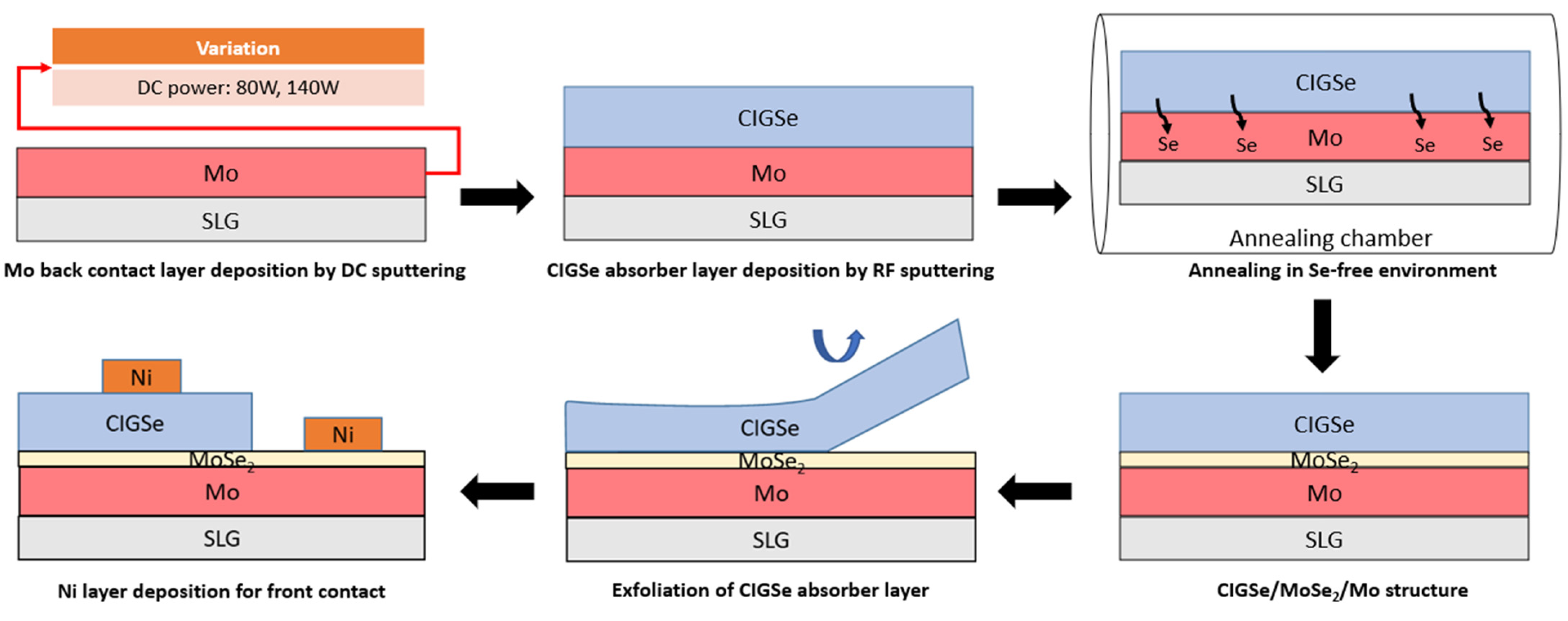
2. Experimental
2.1. Materials and Methods
2.2. Film Characterization
3. Analysis and Discussion
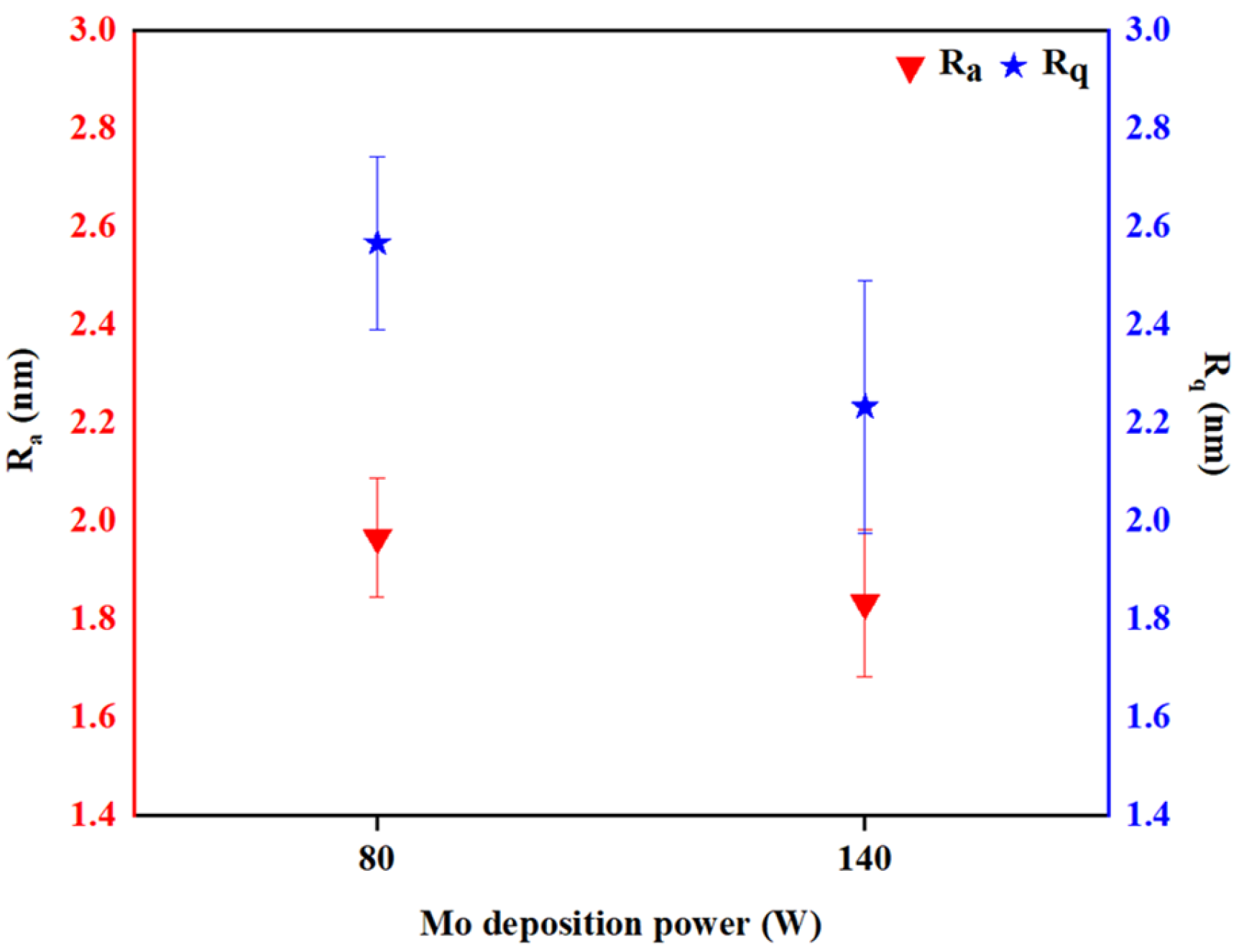
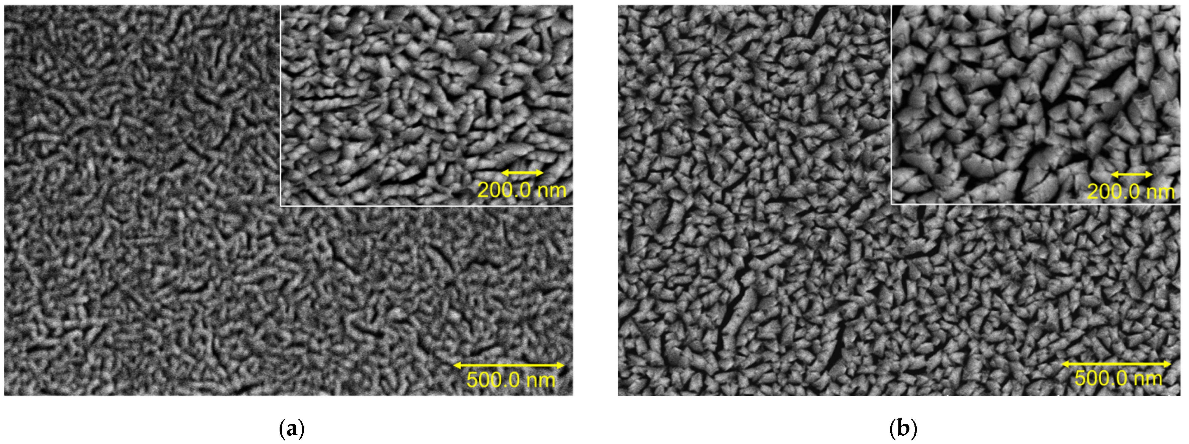
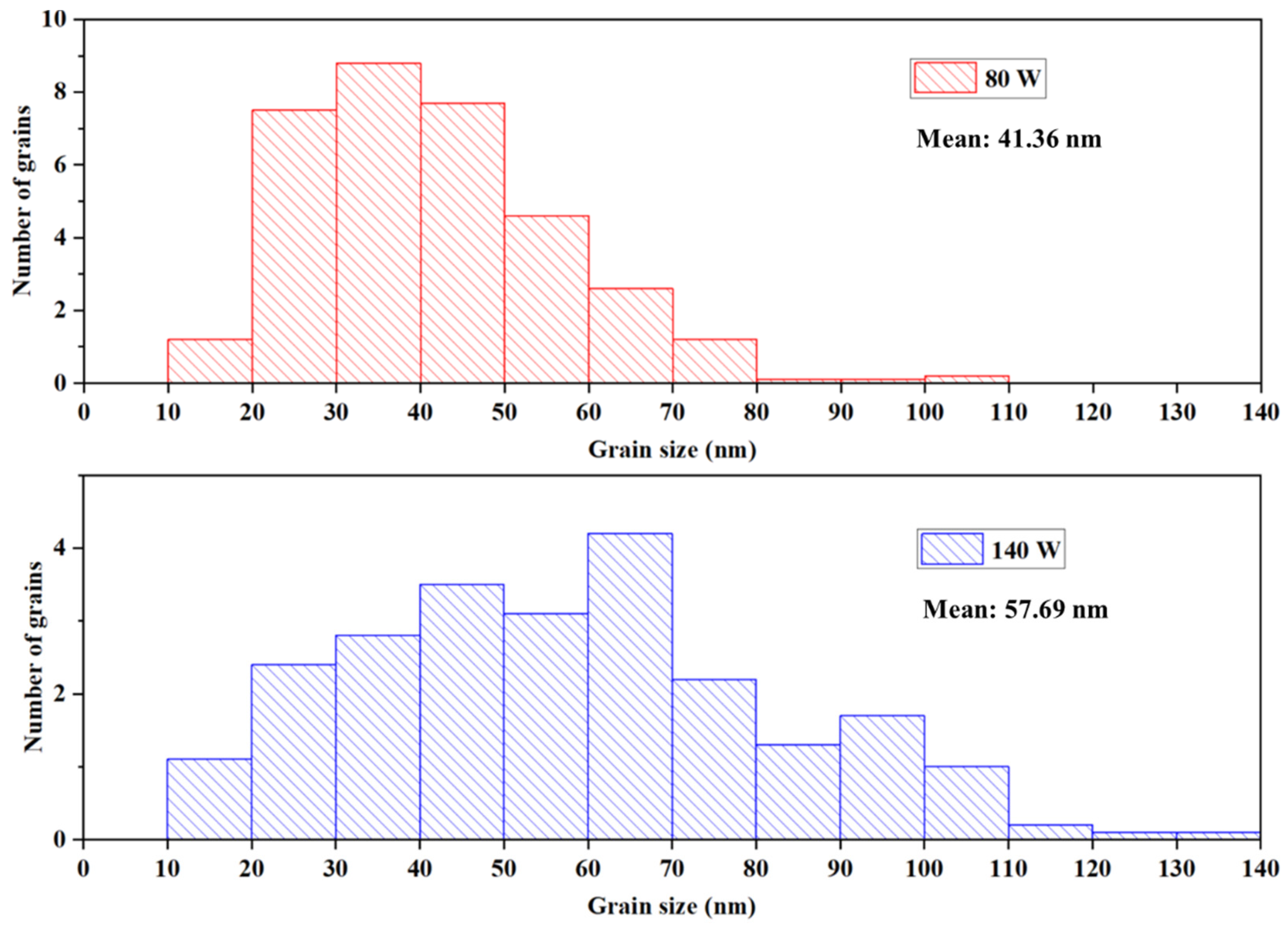
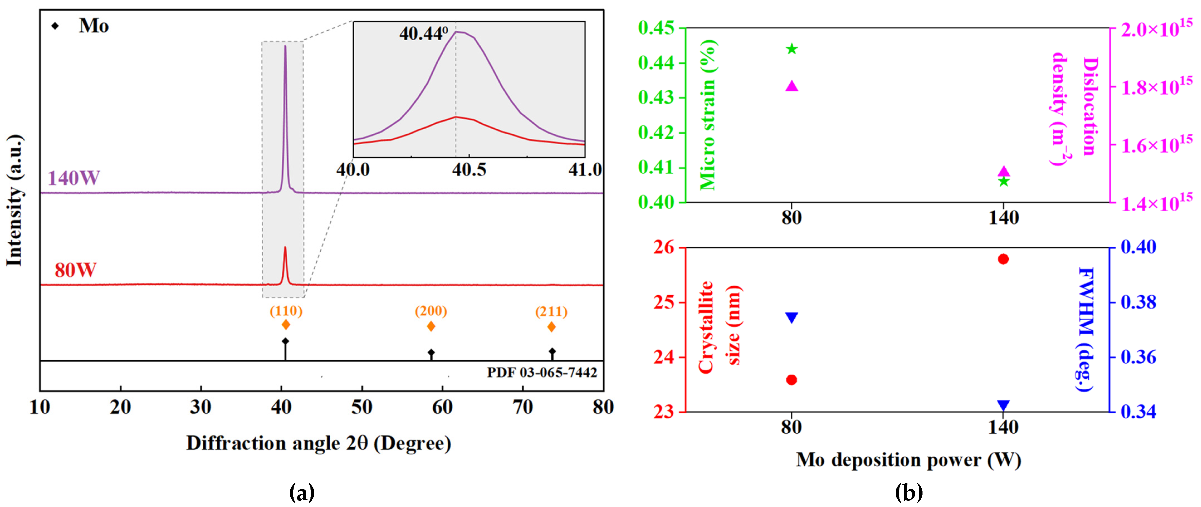
3.1. Mo Film Charactristics with Varied DC Deposition Power
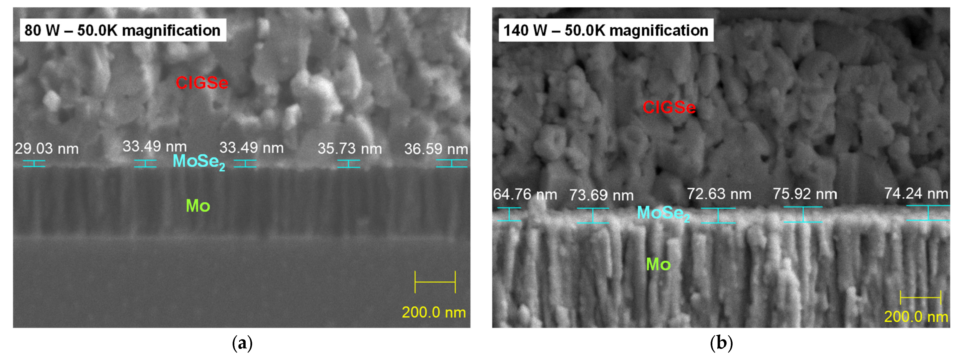
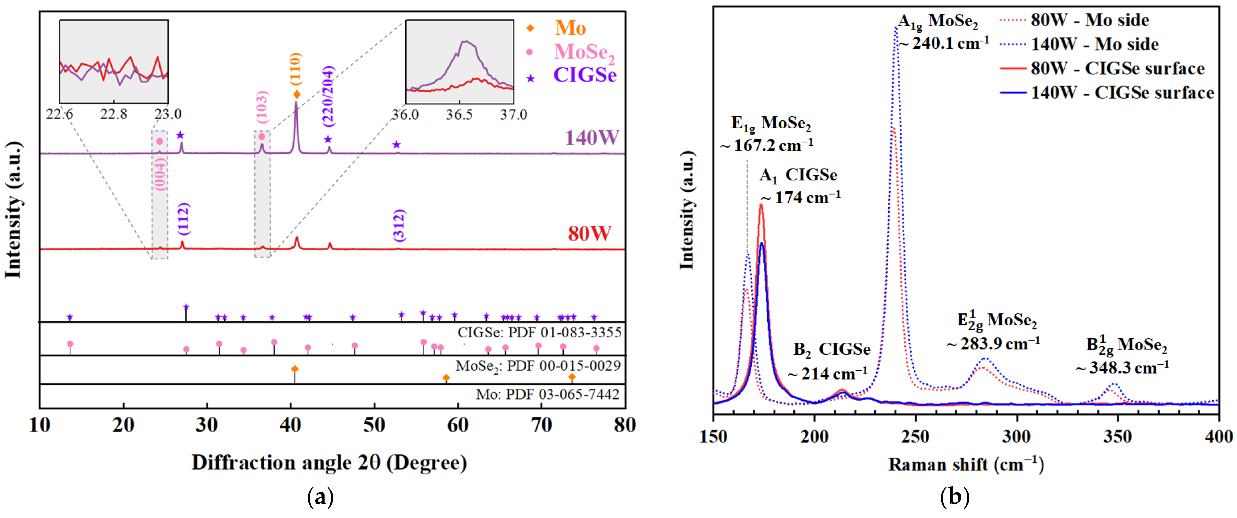
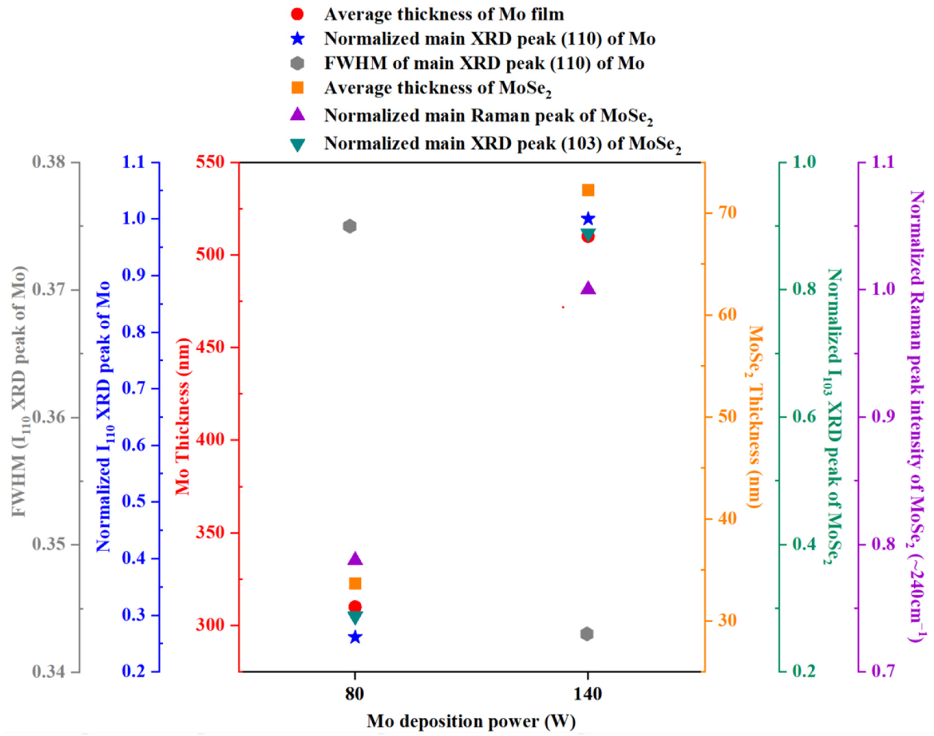
3.2. Correlation between MoSe2 Interfacial Layer Formation and Mo Surface Microstructures
4. Conclusions
Author Contributions
Funding
Institutional Review Board Statement
Informed Consent Statement
Data Availability Statement
Acknowledgments
Conflicts of Interest
References
- Forschen für die Energiewende—Fraunhofer-Institut für Solare Energiesysteme ISE—Fraunhofer ISE. Available online: https://www.ise.fraunhofer.de/ (accessed on 17 November 2022).
- Ramanujam, J.; Singh, U.P. Copper indium gallium selenide based solar cells—A review. Energy Environ. Sci. 2017, 10, 1306–1319. [Google Scholar] [CrossRef]
- Green, M.A.; Dunlop, E.D.; Hohl-Ebinger, J.; Yoshita, M.; Kopidakis, N.; Hao, X. Solar cell efficiency tables (version 59). Prog. Photovolt. Res. Appl. 2022, 30, 3–12. [Google Scholar] [CrossRef]
- Shin, D.; Kim, J.; Gershon, T.; Mankad, R.; Hopstaken, M.; Guha, S.; Ahn, B.T.; Shin, B. Effects of the incorporation of alkali elements on Cu(In,Ga)Se2 thin film solar cells. Sol. Energy Mater. Sol. Cells 2016, 157, 695–702. [Google Scholar] [CrossRef]
- Bansal, N.; Pandey, K.; Singh, K.; Mohanty, B.C. Growth control of molybdenum thin films with simultaneously improved adhesion and conductivity via sputtering for thin film solar cell application. Vacuum 2019, 161, 347–352. [Google Scholar] [CrossRef]
- Orgassa, K.; Schock, H.W.; Werner, J.H. Alternative back contact materials for thin film Cu(In,Ga)Se2 solar cells. Thin Solid Films 2003, 431–432, 387–391. [Google Scholar] [CrossRef]
- Gour, K.S.; Yadav, A.K.; Singh, O.P.; Singh, V.N. Na incorporated improved properties of Cu2ZnSnS4 (CZTS) thin film by DC sputtering. Vacuum 2018, 154, 148–153. [Google Scholar] [CrossRef]
- Scofield, J.H.; Duda, A.; Albin, D.; Ballard, B.L.; Predecki, P.K. Sputtered molybdenum bilayer back contact for copper indium diselenide-based polycrystalline thin-film solar cells. Thin Solid Films 1995, 260, 26–31. [Google Scholar] [CrossRef]
- Pethe, S.A.; Takahashi, E.; Kaul, A.; Dhere, N.G. Effect of sputtering process parameters on film properties of molybdenum back contact. Sol. Energy Mater. Sol. Cells 2012, 100, 1–5. [Google Scholar] [CrossRef]
- Li, Z.H.; Cho, E.S.; Kwon, S.J. Molybdenum thin film deposited by in-line DC magnetron sputtering as a back contact for Cu(In,Ga)Se2 solar cells. Appl. Surf. Sci. 2011, 257, 9682–9688. [Google Scholar] [CrossRef]
- Vink, T.J.; Somers, M.A.J.; Daams, J.L.C.; Dirks, A.G. Stress, strain, and microstructure of sputter-deposited Mo thin films. J. Appl. Phys. 1998, 70, 4301. [Google Scholar] [CrossRef]
- Chelvanathan, P.; Zakaria, Z.; Yusoff, Y.; Akhtaruzzaman, M.; Alam, M.M.; Alghoul, M.A.; Sopian, K.; Amin, N. Annealing effect in structural and electrical properties of sputtered Mo thin film. Appl. Surf. Sci. 2015, 334, 129–137. [Google Scholar] [CrossRef]
- Rashid, H.; Rahman, K.S.; Hossain, M.I.; Nasser, A.A.; Alharbi, F.H.; Akhtaruzzaman, M.; Amin, N. Physical and electrical properties of molybdenum thin films grown by DC magnetron sputtering for photovoltaic application. Results Phys. 2019, 14, 102515. [Google Scholar] [CrossRef]
- Nishiwaki, S.; Kohara, N.; Negami, T.; Nishitani, M.; Wada, T. Characterization of Cu(In,Ga)Se2/Mo Interface in CIGS Solar Cells. MRS Proc. 1997, 485, 139. [Google Scholar] [CrossRef]
- Nishiwaki, S.; Kohara, N.; Negami, T.; Wada, T. MoSe2 layer formation at Cu (In,Ga) Se2/Mo Interfaces in High Efficiency Cu (In1−xGax) Se2 Solar Cells. Jpn. J. Appl. Phys. 1998, 37, L71–L73. [Google Scholar] [CrossRef]
- Kohara, N.; Nishiwaki, S.; Hashimoto, Y.; Negami, T.; Wada, T. Electrical properties of the Cu(In,Ga)Se2/MoSe2/Mo structure. Sol. Energy Mater. Sol. Cells 2001, 67, 209–215. [Google Scholar] [CrossRef]
- Zhu, X.; Zhou, Z.; Wang, Y.; Zhang, L.; Li, A.; Huang, F. Determining factor of MoSe2 formation in Cu(In,Ga)Se2 solar Cells. Sol. Energy Mater. Sol. Cells 2012, 101, 57–61. [Google Scholar] [CrossRef]
- Lin, Y.-C.; Shen, M.-T.; Chen, Y.-L.; Hsu, H.-R.; Wu, C.-H. A study on MoSe2 layer of Mo contact in Cu(In,Ga)Se2 thin film solar cells. Thin Solid Films 2014, 570, 166–171. [Google Scholar] [CrossRef]
- Abou-Ras, D.; Kostorz, G.; Bremaud, D.; Kälin, M.; Kurdesau, F.V.; Döbeli, M. Formation and characterisation of MoSe2 for Cu(In,Ga)Se2 based solar cells. Thin Solid Films 2005, 480–481, 433–438. [Google Scholar] [CrossRef]
- Yoon, J.-H.; Kim, J.-H.; Kim, W.M.; Park, J.-K.; Baik, Y.-J.; Seong, T.-Y.; Jeong, J. Electrical properties of CIGS/Mo junctions as a function of MoSe 2 orientation and Na doping. Prog. Photovolt. Res. Appl. 2014, 22, 90–96. [Google Scholar] [CrossRef]
- Liu, Y.-J.; Ou, C.-Y.; Lu, C.-H. Effects of Mo films prepared via different sputtering conditions on the formation of MoSe2 during selenization. J. Alloys Compd. 2018, 747, 621–628. [Google Scholar] [CrossRef]
- Zhou, D.; Zhu, H.; Liang, X.; Zhang, C.; Li, Z.; Xu, Y.; Chen, J.; Zhang, L.; Mai, Y. Sputtered molybdenum thin films and the application in CIGS solar cells. Appl. Surf. Sci. 2016, 362, 202–209. [Google Scholar] [CrossRef]
- Frindt, R.F. Single Crystals of MoS2 Several Molecular Layers Thick. J. Appl. Phys. 2004, 37, 1928. [Google Scholar] [CrossRef]
- Varghese, S.; Reig, D.S.; Mehew, J.D.; Block, A.; El Sachat, A.; Chávez-Ángel, E.; Sledzinska, M.; Ballesteros, B.; Sotomayor Torres, C.M.; Tielrooij, K.J. Fabrication and characterization of large-area suspended MoSe2 crystals down to the monolayer. J. Phys. Mater. 2021, 4, 046001. [Google Scholar] [CrossRef]
- Peng, B.; Ang, P.K.; Loh, K.P. Two-dimensional dichalcogenides for light-harvesting applications. Nano Today 2015, 10, 128–137. [Google Scholar] [CrossRef]
- Yu, X.; Sivula, K. Toward Large-Area Solar Energy Conversion with Semiconducting 2D Transition Metal Dichalcogenides. ACS Energy Lett. 2016, 1, 315–322. [Google Scholar] [CrossRef]
- Feng, W.; Zheng, W.; Chen, X.; Liu, G.; Cao, W.; Hu, P. Solid-state reaction synthesis of a InSe/CuInSe2 lateral p-n heterojunction and application in high performance optoelectronic devices. Chem. Mater. 2015, 27, 983–989. [Google Scholar] [CrossRef]
- Balendhran, S.; Walia, S.; Nili, H.; Ou, J.Z.; Zhuiykov, S.; Kaner, R.B.; Sriram, S.; Bhaskaran, M.; Kalantar-Zadeh, K. Two-Dimensional Molybdenum Trioxide and Dichalcogenides. Adv. Funct. Mater. 2013, 23, 3952–3970. [Google Scholar] [CrossRef]
- Weinhardt, L.; Fuchs, O.; Peter, A.; Umbach, E.; Heske, C.; Reichardt, J.; Bär, M.; Lauermann, I.; Kötschau, I.; Grimm, A.; et al. Spectroscopic investigation of the deeply buried Cu(In,Ga)(S,Se)2/Mo interface in thin-film solar cells. J. Chem. Phys. 2006, 124, 074705. [Google Scholar] [CrossRef] [Green Version]
- Weinhardt, L.; Blum, M.; Bär, M.; Heske, C.; Fuchs, O.; Umbach, E.; Denlinger, J.D.; Ramanathan, K.; Noufi, R. Chemical properties of the Cu(In,Ga)Se2/Mo/glass interfaces in thin film solar cells. Thin Solid Films 2007, 515, 6119–6122. [Google Scholar] [CrossRef]
- Bhang, S.J.; Kim, H.; Kim, K.R.; Park, J. Boron Nitride-Based Paint with High Heat Dissipation Performance. Phys. Status Solidi 2019, 216, 1800512. [Google Scholar] [CrossRef]
- Ahmed, N.; Iqbal, M.A.; Khan, Z.S.; Qayyum, A.A. DC Magnetron-Sputtered Mo Thin Films with High Adhesion, Conductivity and Reflectance. J. Electron. Mater. 2020, 49, 4221–4230. [Google Scholar] [CrossRef]
- Wada, T.; Kohara, N.; Nishiwaki, S.; Negami, T. Characterization of the Cu(In,Ga)Se2/Mo interface in CIGS solar cells. Thin Solid Films 2001, 387, 118–122. [Google Scholar] [CrossRef]
- Aqil, M.M.; Azam, M.A.; Aziz, M.F.; Latif, R. Deposition and characterization of molybdenum thin film using direct current magnetron and atomic force microscopy. J. Nanotechnol. 2017, 2017, 4862087. [Google Scholar] [CrossRef] [Green Version]
- Kashyout, A.E.H.B.; Soliman, H.M.A.; Gabal, H.A.; Ibrahim, P.A.; Fathy, M. Preparation and characterization of DC sputtered molybdenum thin films. Alexandria Eng. J. 2011, 50, 57–63. [Google Scholar] [CrossRef] [Green Version]
- Doroody, C.; Rahman, K.S.; Rosly, H.N.; Harif, M.N.; Isah, M.; Kar, Y.B.; Tiong, S.K.; Amin, N. A comparative study of CdS thin films grown on ultra-thin glass substrates by RF magnetron sputtering and chemical bath deposition. Mater. Sci. Semicond. Process. 2021, 133, 105935. [Google Scholar] [CrossRef]
- Wilson, G.J.; Matijasevich, A.S.; Mitchell, D.R.G.; Schulz, J.C.; Will, G.D. Modification of TiO2 for enhanced surface properties: Finite ostwald ripening by a microwave hydrothermal process. Langmuir 2006, 22, 2016–2027. [Google Scholar] [CrossRef]
- Briot, O.; Moret, M.; Barbier, C.; Tiberj, A.; Peyre, H.; Sagna, A.; Contreras, S. Optimization of the properties of the molybdenum back contact deposited by radiofrequency sputtering for Cu(In1−xGax)Se2 solar cells. Sol. Energy Mater. Sol. Cells 2018, 174, 418–422. [Google Scholar] [CrossRef]
- Daniel, R.; Holec, D.; Bartosik, M.; Keckes, J.; Mitterer, C. Size effect of thermal expansion and thermal/intrinsic stresses in nanostructured thin films: Experiment and model. Acta Mater. 2011, 59, 6631–6645. [Google Scholar] [CrossRef]
- Mayadas, A.F.; Shatzkes, M. Electrical-Resistivity Model for Polycrystalline Films: The Case of Arbitrary Reflection at External Surfaces. Phys. Rev. B 1970, 1, 1382. [Google Scholar] [CrossRef]
- Gulkowski, S.; Krawczak, E. RF/DC Magnetron Sputtering Deposition of Thin Layers for Solar Cell Fabrication. Coatings 2020, 10, 791. [Google Scholar] [CrossRef]
- Gordillo, G.; Mesa, F.; Calderón, C. Electrical and Morphological Properties of Low Resistivity Mo thin Films Prepared by Magnetron Sputtering. Brazilian J. Phys. 2006, 36, 982–985. [Google Scholar] [CrossRef] [Green Version]
- Yoon, J.H.; Yoon, K.H.; Kim, J.K.; Kim, W.M.; Park, J.K.; Lee, T.S.; Baik, Y.J.; Seong, T.Y.; Jeong, J.H. Effect of the Mo back contact microstructure on the preferred orientation of CIGS thin films. In Proceedings of the 2010 35th IEEE Photovoltaic Specialists Conference, Honolulu, HI, USA, 20–25 June 2010; pp. 2443–2447. [Google Scholar] [CrossRef]
- Sugai, S.; Ueda, T. High-pressure Raman spectroscopy in the layered materials 2H-MoS2, 2H-MoSe2, and 2H-MoTe2. Phys. Rev. B 1982, 26, 6554. [Google Scholar] [CrossRef]
- Sekine, T.; Izumi, M.; Nakashizu, T.; Uchinokura, K.; Matsuura, E. Raman Scattering and Infrared Reflectance in 2H-MoSe2. J. Phys. Soc. Jpn. 2013, 49, 1069–1077. [Google Scholar] [CrossRef]
- Roy, S.; Guha, P.; Kundu, S.N.; Hanzawa, H.; Chaudhuri, S.; Pal, A.K. Characterization of Cu(In,Ga)Se2 films by Raman scattering. Mater. Chem. Phys. 2002, 73, 24–30. [Google Scholar] [CrossRef]
- Wada, T.; Kohara, N.; Negami, T.; Nishitani, M. Chemical and Structural Characterization of Cu(In,Ga)Se2/Mo Interface in Cu(In,Ga)Se2 Solar Cells. Jpn. J. Appl. Phys. 1996, 35, L1253. [Google Scholar] [CrossRef]
- Li, W.; Yan, X.; Aberle, A.G.; Venkataraj, S. Effect of sodium diffusion on the properties of CIGS solar absorbers prepared using elemental Se in a two-step process. Sci. Rep. 2019, 9, 1–11. [Google Scholar] [CrossRef] [Green Version]
- Zhang, L.; Zhuang, D.; Zhao, M.; Gong, Q.; Guo, L.; Ouyang, L.; Sun, R.; Wei, Y.; Zhan, S. The effects of annealing temperature on CIGS solar cells by sputtering from quaternary target with Se-free post annealing. Appl. Surf. Sci. 2017, 413, 175–180. [Google Scholar] [CrossRef]
- Nakada, T. Microstructural and diffusion properties of CIGS thin film solar cells fabricated using transparent conducting oxide back contacts. Thin Solid Films 2005, 480–481, 419–425. [Google Scholar] [CrossRef]
- Valencia, D.; Conde, J.; Ashok, A.; Meza-Avendaño, C.A.; Vilchis, H.; Velumani, S. Optimization of Cu(In, Ga)Se2 (CIGSe) thin film solar cells parameters through numerical simulation and experimental study. Sol. Energy 2021, 224, 298–308. [Google Scholar] [CrossRef]
- Kamikawa, Y.; Nishinaga, J.; Shibata, H.; Ishizuka, S. Efficient Narrow Band Gap Cu(In,Ga)Se2 Solar Cells with Flat Surface. ACS Appl. Mater. Interfaces 2020, 12, 45485–45492. [Google Scholar] [CrossRef]
- Zhao, H.; Xie, J.; Mao, A. Effects of Bottom Layer Sputtering Pressures and Annealing Temperatures on the Microstructures, Electrical and Optical Properties of Mo Bilayer Films Deposited by RF/DC Magnetron Sputtering. Appl. Sci. 2019, 9, 1395. [Google Scholar] [CrossRef] [Green Version]
- Chelvanathan, P.; Hossain, M.I.; Husna, J.; Alghoul, M.; Sopian, K.; Amin, N. Effects of Transition Metal Dichalcogenide Molybdenum Disulfide Layer Formation in Copper–Zinc–Tin–Sulfur Solar Cells from Numerical Analysis. Jpn. J. Appl. Phys. 2012, 51, 10NC32. [Google Scholar] [CrossRef]
- Chelvanathan, P.; Shahahmadi, S.A.; Ferdaous, M.T.; Sapeli, M.M.I.; Sopian, K.; Amin, N. Controllable formation of MoS2 via preferred crystallographic orientation modulation of DC-sputtered Mo thin film. Mater. Lett. 2018, 219, 174–177. [Google Scholar] [CrossRef]


| Sample Identification | DC Power (W) | DC Power Density (W/cm2) | Deposition Time (Minute) | Film Thickness (nm) | Detachment Percentage (%) | ISO Damage Level 1 | Performance |
|---|---|---|---|---|---|---|---|
| Mo-80 | 80 | 4 | 60 | 310 | <5% | 1 | Pass |
| Mo-140 | 140 | 7 | 60 | 510 | 35~65% | 4 | Fail |
| Sample | Mo-80 | Mo-140 |
|---|---|---|
| Ra (nm) | 1.97 | 1.83 |
| Rq (nm) | 2.57 | 2.23 |
| Rq/Ra | 1.30 | 1.22 |
| Rsk | 0.48 | −1.06 |
| Sample | (deg) | (Å) | (Å) | (nm) | (×10−3) | (×1011) | ||
|---|---|---|---|---|---|---|---|---|
| Mo-80 | (110) | 20.22 | 0.375 | 3.152 | 0.223 | 23.59 | 4.44 | 1.80 |
| Mo-140 | (110) | 20.22 | 0.343 | 3.152 | 0.223 | 25.79 | 4.06 | 1.50 |
| Sample | Carrier Concentration (cm−3) | Mobility (cm2/Vs) | Resistivity (μΩ·cm) | Sheet Resistance (Ω/square) | Reference Values for Sheet Resistance (Ω/Square) 1 |
|---|---|---|---|---|---|
| Mo-80 | 5.29 × 10²² | 1.62 | 23.158 | 0.747 | 2.5 |
| Mo-140 | 5.86 × 10²² | 6.80 | 17.982 | 0.353 | 0.3 |
Disclaimer/Publisher’s Note: The statements, opinions and data contained in all publications are solely those of the individual author(s) and contributor(s) and not of MDPI and/or the editor(s). MDPI and/or the editor(s) disclaim responsibility for any injury to people or property resulting from any ideas, methods, instructions or products referred to in the content. |
© 2023 by the authors. Licensee MDPI, Basel, Switzerland. This article is an open access article distributed under the terms and conditions of the Creative Commons Attribution (CC BY) license (https://creativecommons.org/licenses/by/4.0/).
Share and Cite
Za’abar, F.‘I.; Mahmood Zuhdi, A.W.; Doroody, C.; Chelvanathan, P.; Yusoff, Y.; Abdullah, S.F.; Bahrudin, M.S.; Wan Adini, W.S.; Ahmad, I.; Wan Abdullah, W.S.; et al. Probing the Interplay between Mo Back Contact Layer Deposition Condition and MoSe2 Layer Formation at the CIGSe/Mo Hetero-Interface. Materials 2023, 16, 2497. https://doi.org/10.3390/ma16062497
Za’abar F‘I, Mahmood Zuhdi AW, Doroody C, Chelvanathan P, Yusoff Y, Abdullah SF, Bahrudin MS, Wan Adini WS, Ahmad I, Wan Abdullah WS, et al. Probing the Interplay between Mo Back Contact Layer Deposition Condition and MoSe2 Layer Formation at the CIGSe/Mo Hetero-Interface. Materials. 2023; 16(6):2497. https://doi.org/10.3390/ma16062497
Chicago/Turabian StyleZa’abar, Fazliyana ‘Izzati, Ahmad Wafi Mahmood Zuhdi, Camellia Doroody, Puvaneswaran Chelvanathan, Yulisa Yusoff, Siti Fazlili Abdullah, Mohd. Shaparuddin Bahrudin, Wan Sabeng Wan Adini, Ibrahim Ahmad, Wan Syakirah Wan Abdullah, and et al. 2023. "Probing the Interplay between Mo Back Contact Layer Deposition Condition and MoSe2 Layer Formation at the CIGSe/Mo Hetero-Interface" Materials 16, no. 6: 2497. https://doi.org/10.3390/ma16062497