
High Refractive Index Silica-Titania Films Fabricated via the Sol–Gel Method and Dip-Coating Technique—Physical and Chemical Characterization

 , ,
, ,  , , , and
Abstract
:1. Introduction
2. Technology
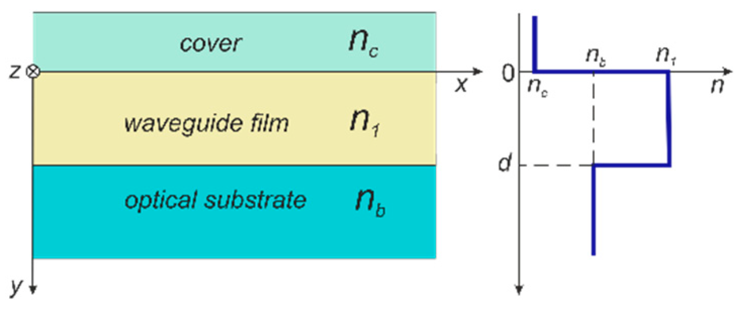
2.1. Fundamentals
2.2. Materials
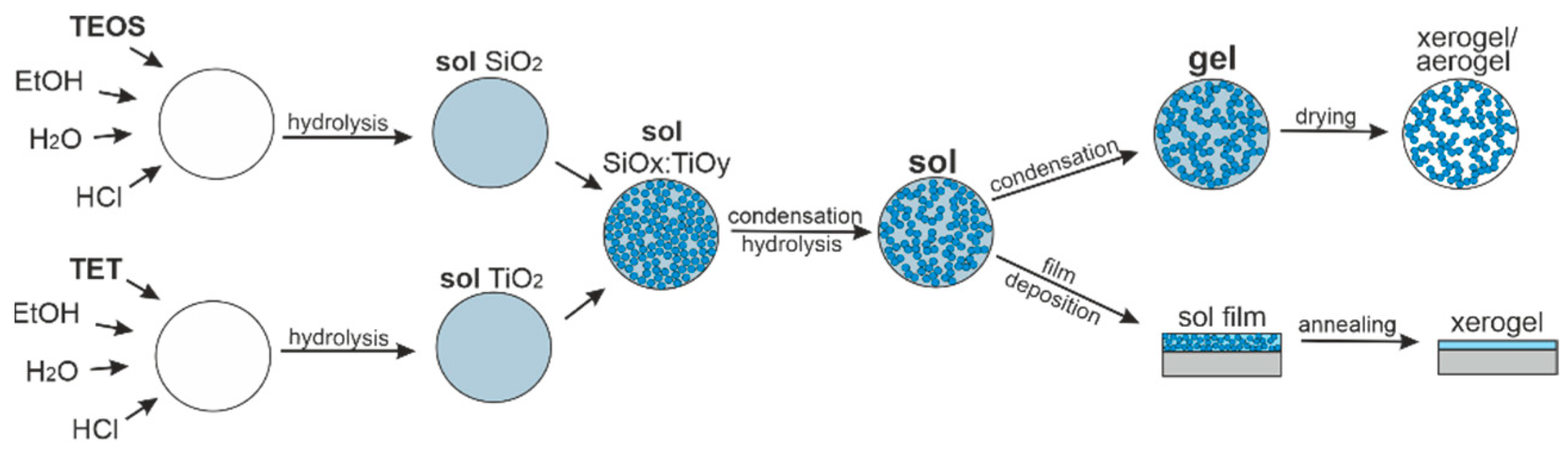
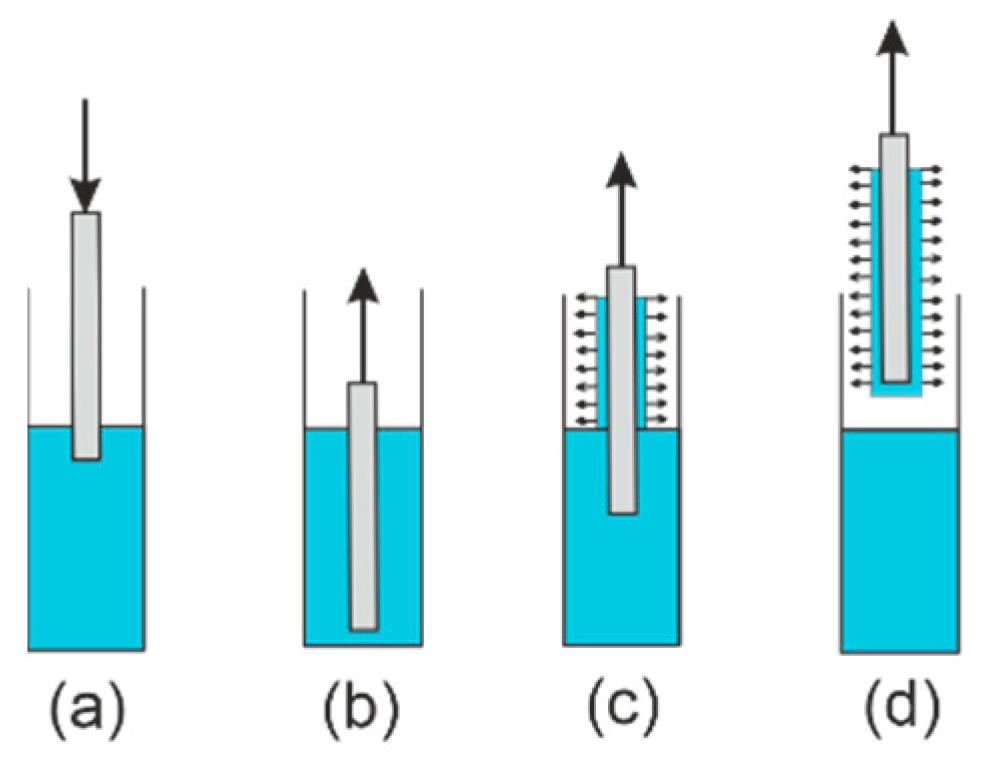
2.3. Sol Preparation and Film Fabrication
3. Methods and Materials
3.1. Fourier Transform Infrared Spectroscopy
3.2. Raman Spectroscopy
3.3. Spectrophotometry
3.4. Ellipsometry
3.5. Surface Morphology
4. Results and Discussion
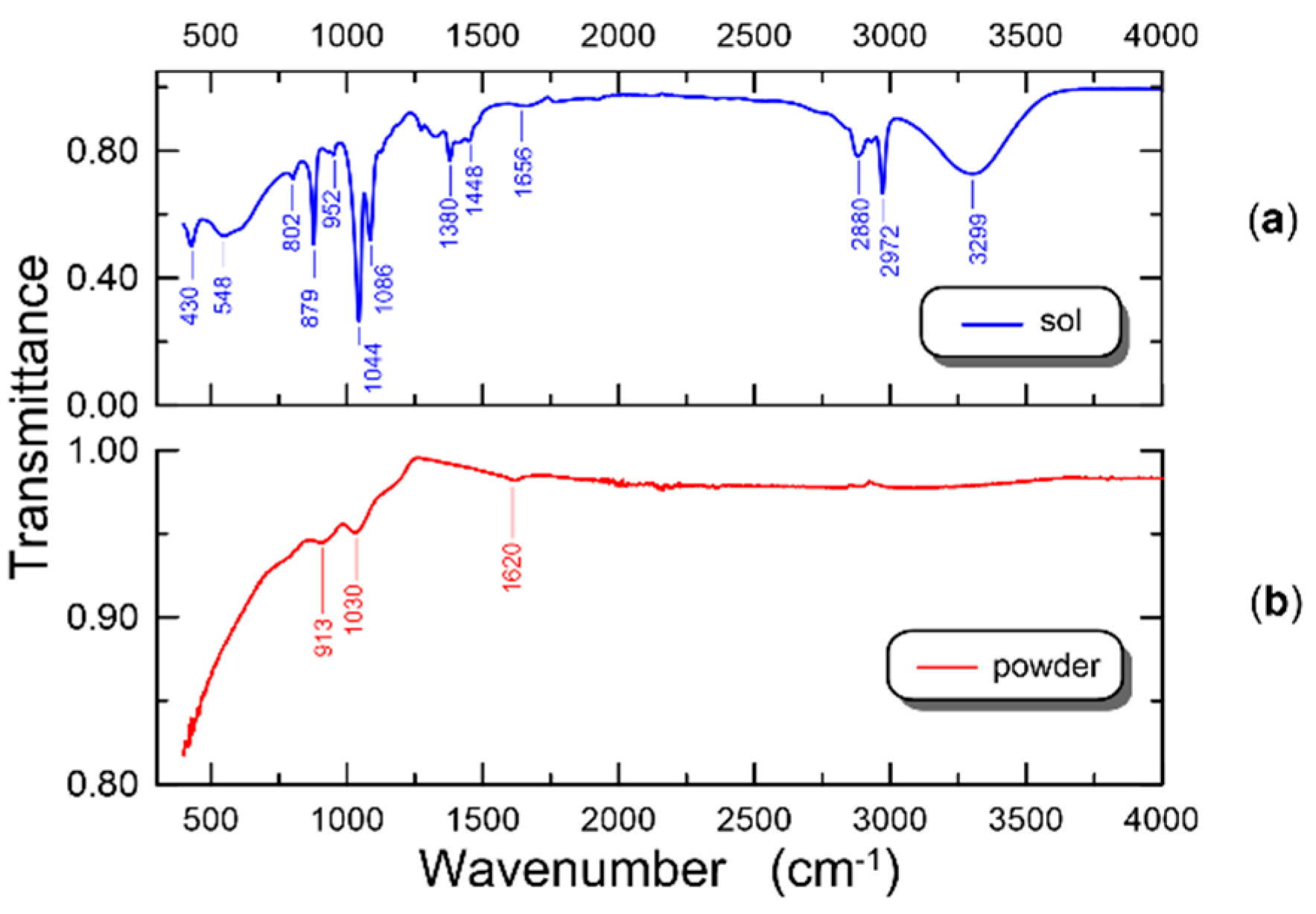
4.1. FTIR
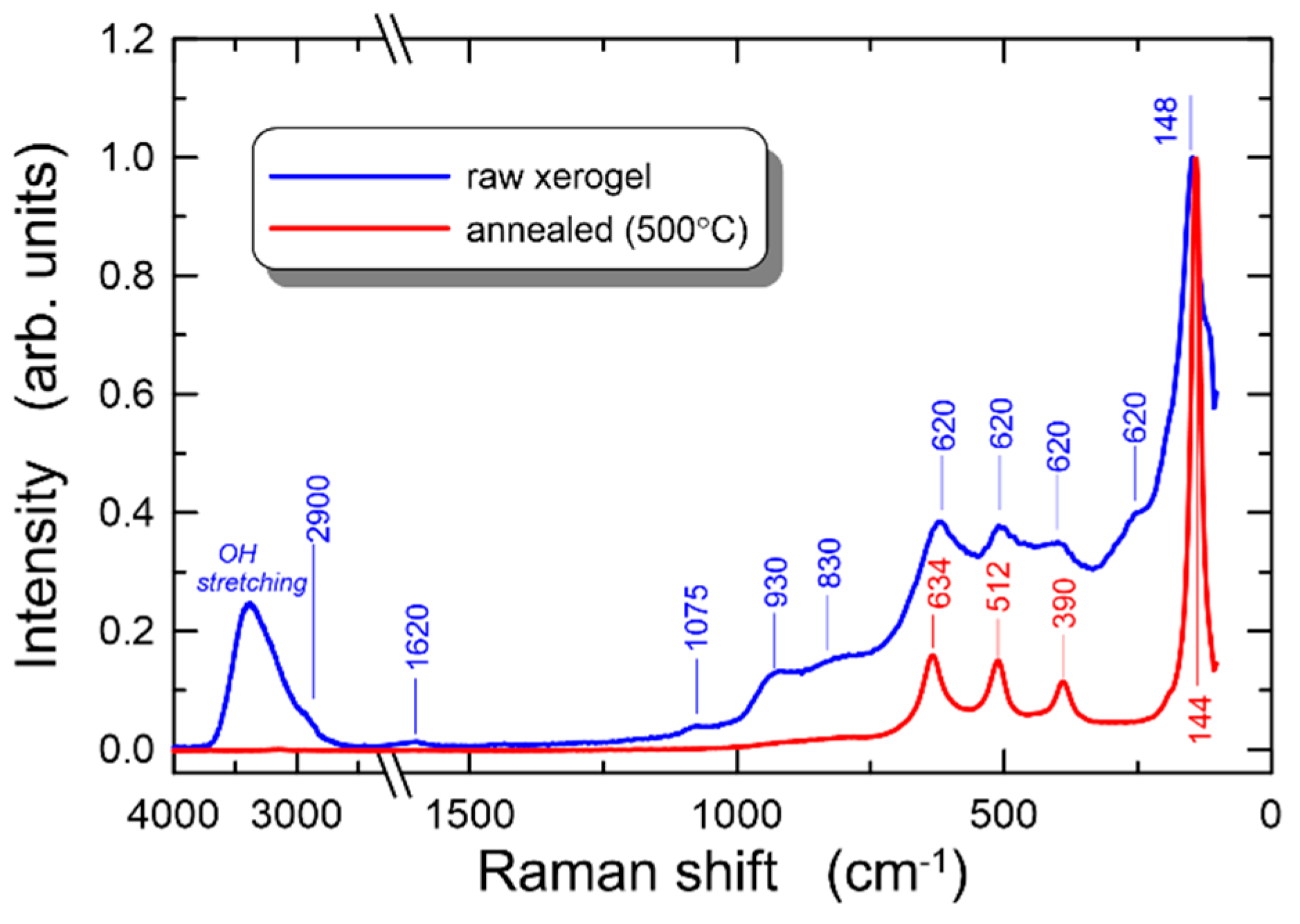
4.2. Raman Spectroscopy
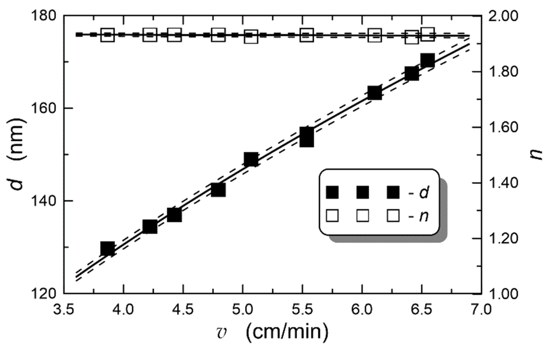
4.3. Effect of Withdrawal Speed
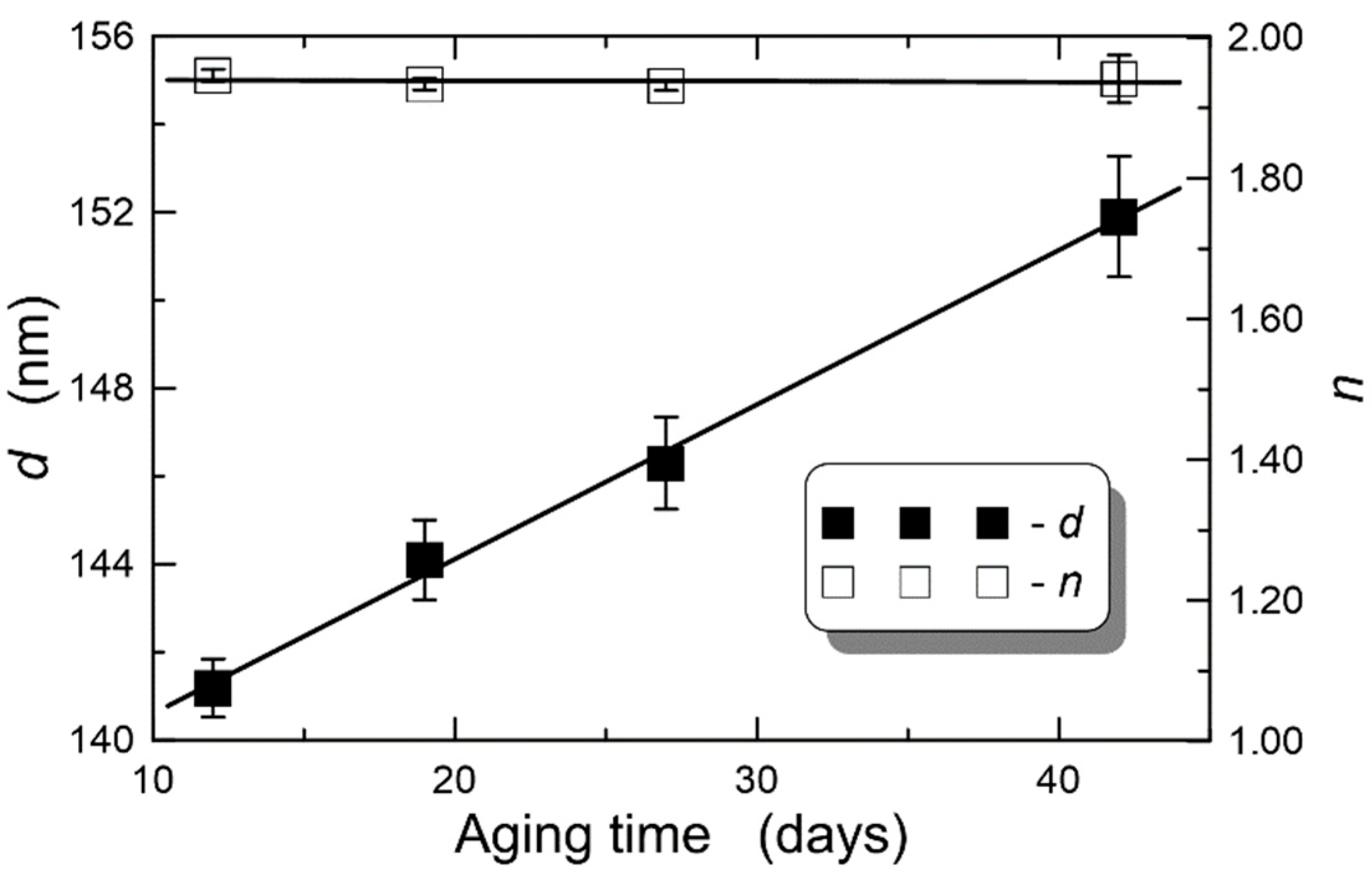
4.4. Effect of Sol Aging
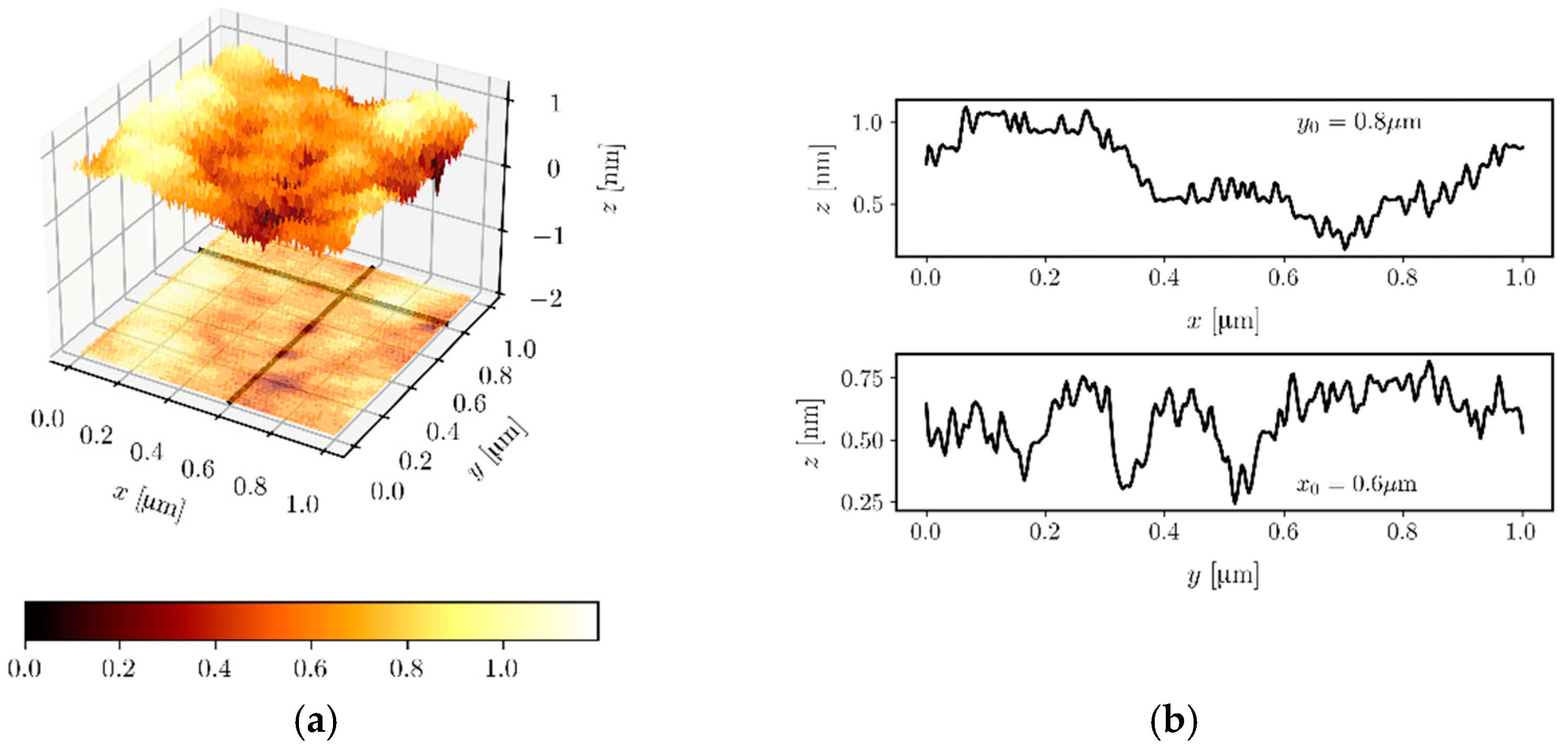
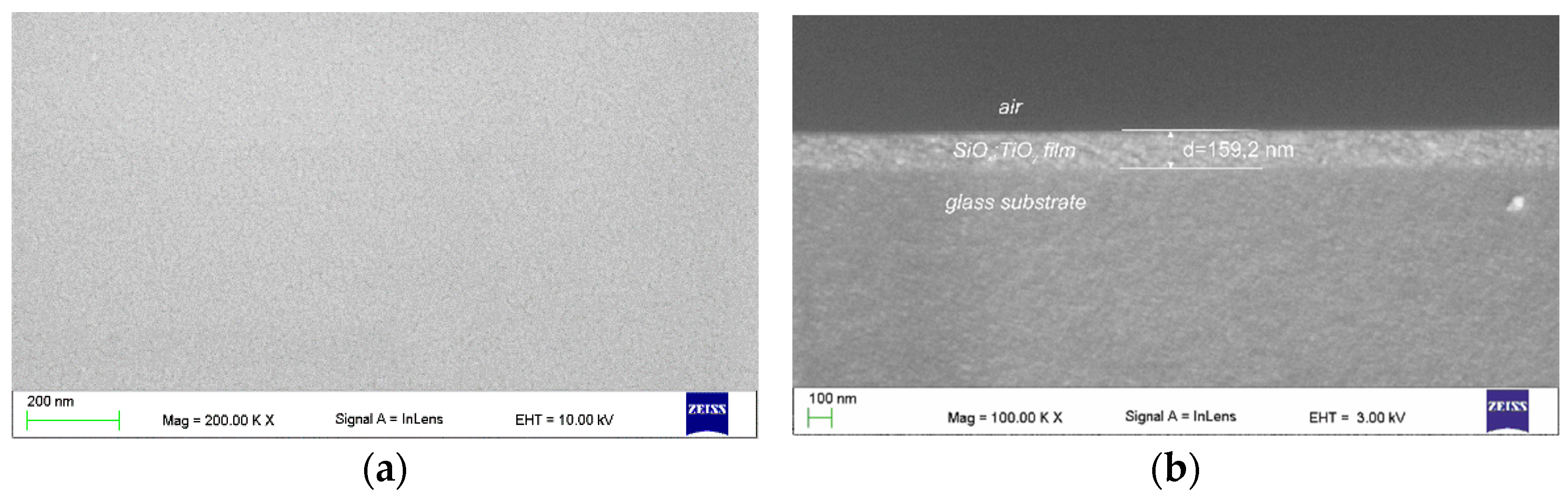
4.5. Surface Morphology
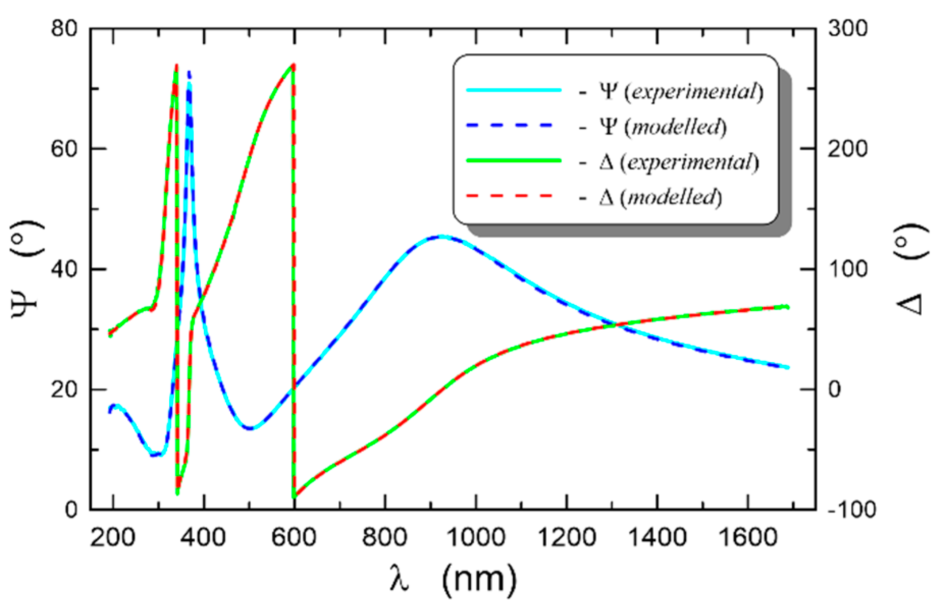
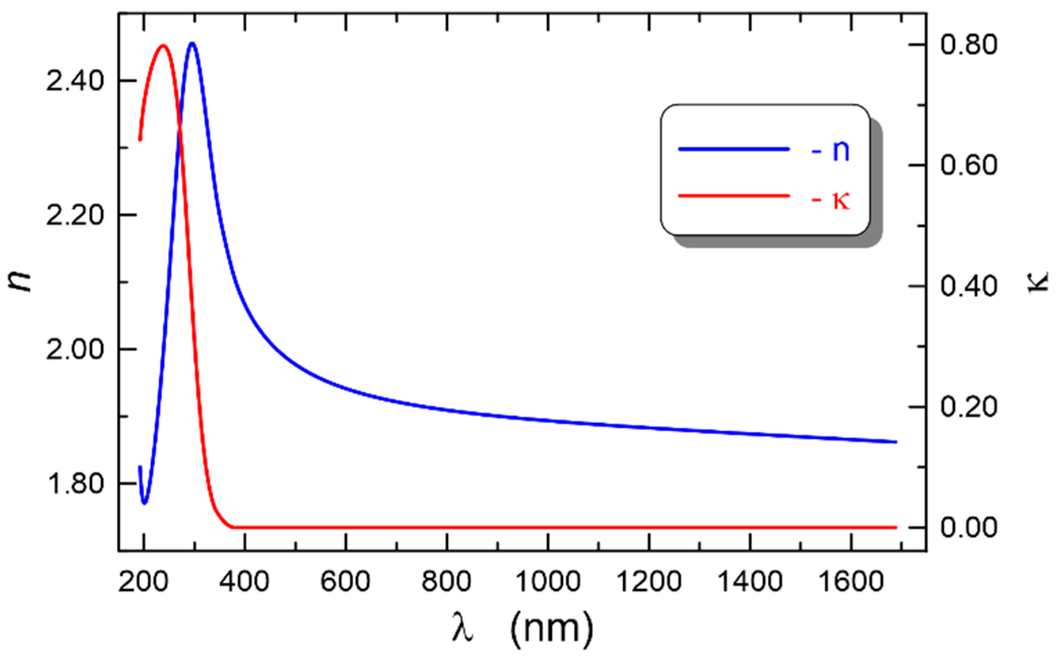
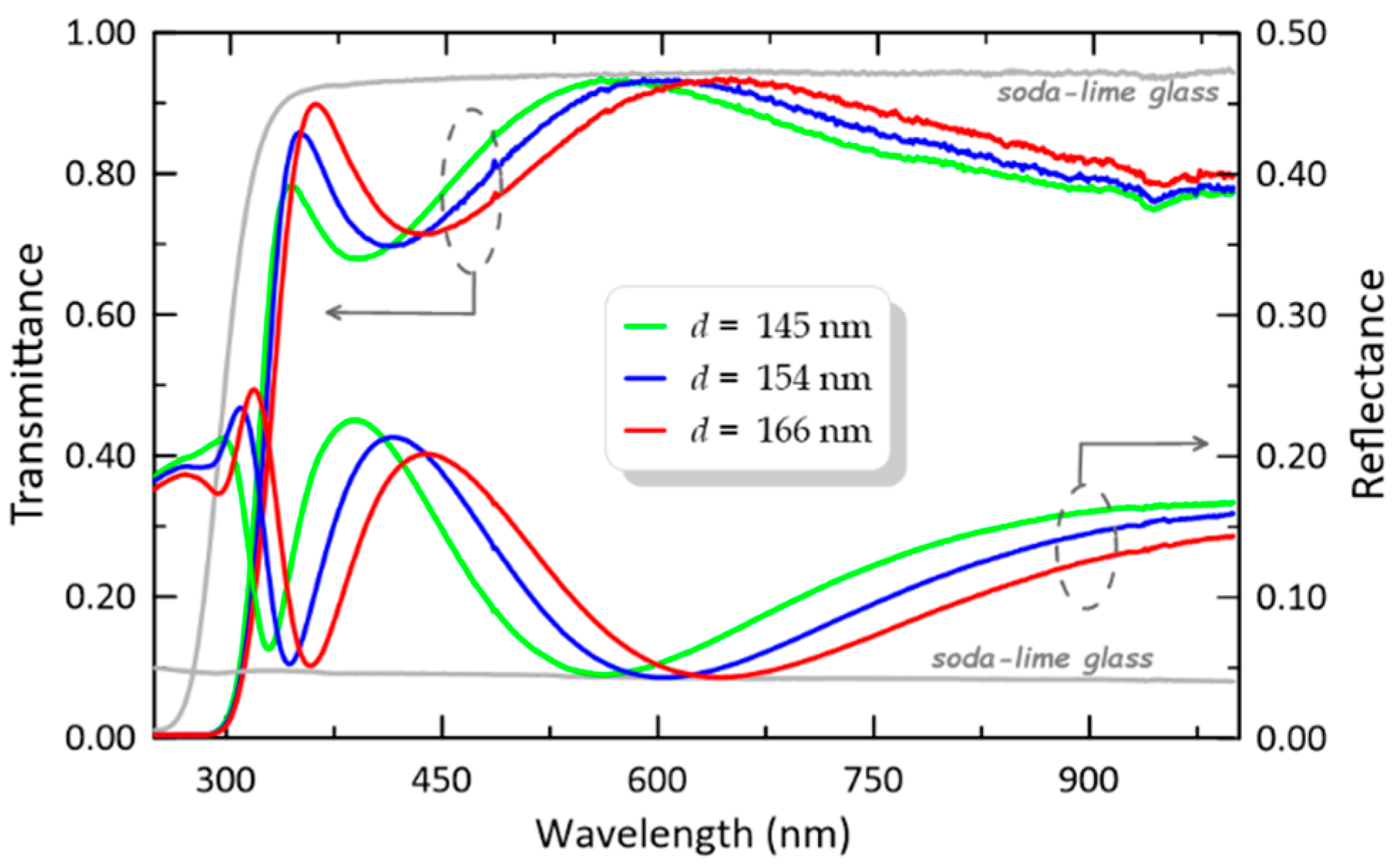
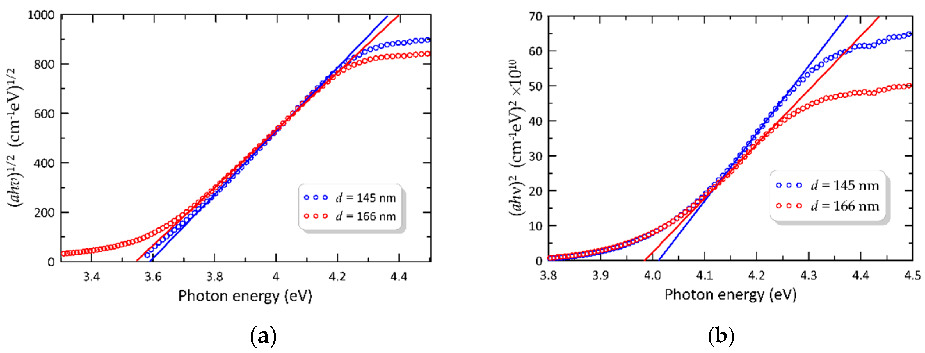
4.6. Optical Properties
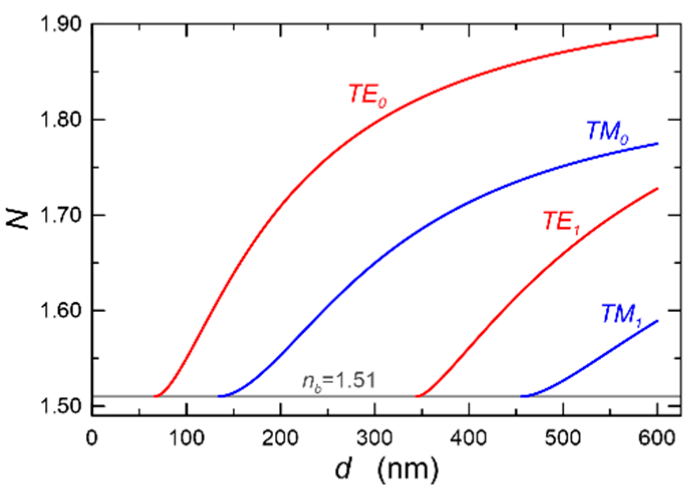
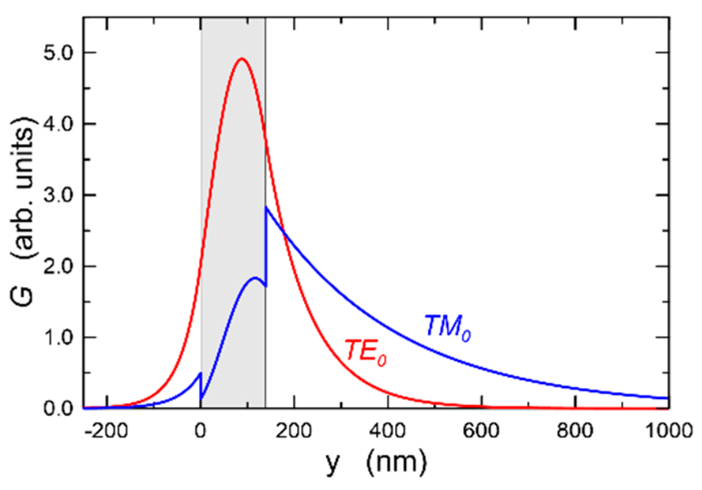
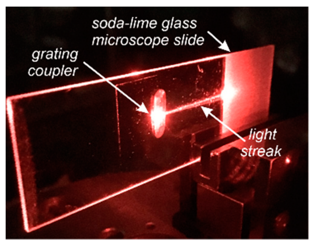
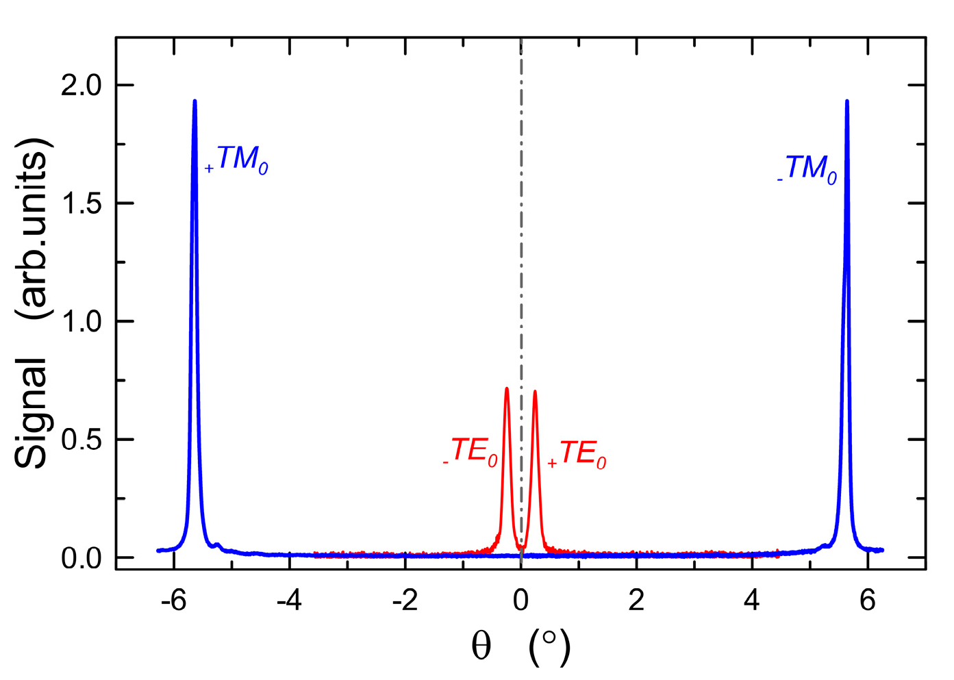
4.7. Waveguide Properties
5. Conclusions
Author Contributions
Funding
Institutional Review Board Statement
Informed Consent Statement
Data Availability Statement
Acknowledgments
Conflicts of Interest
References
- Edlou, S.M.; Smajkiewicz, A.; Al-Jumaily, G.A. Optical properties and environmental stability of oxide coatings deposited by reactive sputtering. Appl. Opt. 1993, 32, 5601. [Google Scholar] [CrossRef]
- Eiamchai, P.; Chindaudom, P.; Pokaipisit, A.; Limsuwan, P. A spectroscopic ellipsometry study of TiO2 thin films prepared by ion-assisted electron-beam evaporation. Curr. Appl. Phys. 2009, 9, 707–712. [Google Scholar] [CrossRef]
- Kailasa Ganapathi, S.; Kaur, M.; Shaheera, M.; Pathak, A.; Gadkari, S.C.; Debnath, A.K. Highly sensitive NO2 sensor based on ZnO nanostructured thin film prepared by SILAR technique. Sens. Actuators B Chem. 2021, 335, 129678. [Google Scholar] [CrossRef]
- Fadel, M.; Azim, M.; Omer, O.A.; Basily, R.R. A study of some optical properties of hafnium dioxide (HfO2) thin films and their applications. Appl. Phys. A 1998, 66, 335–343. [Google Scholar] [CrossRef]
- Luo, X.; Li, Y.; Yang, H.; Liang, Y.; He, K.; Sun, W.; Lin, H.-H.; Yao, S.; Lu, X.; Wan, L.; et al. Investigation of HfO2 thin films on Si by X-ray photoelectron spectroscopy, rutherford backscattering, grazing incidence X-ray diffraction and variable angle spectroscopic ellipsometry. Crystals 2018, 8, 248. [Google Scholar] [CrossRef] [Green Version]
- Boratto, M.H.; Congiu, M.; dos Santos, S.B.O.; Scalvi, L.V.A. Annealing temperature influence on sol-gel processed zirconium oxide thin films for electronic applications. Ceram. Int. 2018, 44, 10790–10796. [Google Scholar] [CrossRef] [Green Version]
- Venkataraj, S.; Kappertz, O.; Weis, H.; Drese, R.; Jayavel, R.; Wuttig, M. Structural and optical properties of thin zirconium oxide films prepared by reactive direct current magnetron sputtering. J. Appl. Phys. 2002, 92, 3599–3607. [Google Scholar] [CrossRef]
- Bright, T.J.; Watjen, J.I.; Zhang, Z.M.; Muratore, C.; Voevodin, A.A.; Koukis, D.I.; Tanner, D.B.; Arenas, D.J. Infrared optical properties of amorphous and nanocrystalline Ta2O5 thin films. J. Appl. Phys. 2013, 114, 083515. [Google Scholar] [CrossRef]
- Nisar, J.; Topalian, Z.; De Sarkar, A.; Österlund, L.; Ahuja, R. TiO2-based gas sensor: A possible application to SO2. ACS Appl. Mater. Interfaces 2013, 5, 8516–8522. [Google Scholar] [CrossRef]
- Shamma, K.; Aldwayyan, A.; Albrithen, H.; Alodhayb, A. Exploiting the properties of TiO2 thin films as a sensing layer on (MEMS)-based sensors for radiation dosimetry applications. AIP Adv. 2021, 11, 025209. [Google Scholar] [CrossRef]
- Mitra, P.; Chatterjee, A.P.; Maiti, H.S. ZnO thin film sensor. Mater. Lett. 1998, 35, 33–38. [Google Scholar] [CrossRef]
- Kolhe, P.S.; Shinde, A.B.; Kulkarni, S.G.; Maiti, N.; Koinkar, P.M.; Sonawane, K.M. Gas sensing performance of Al doped ZnO thin film for H2S detection. J. Alloys Compd. 2018, 748, 6–11. [Google Scholar] [CrossRef]
- Ma, H.; Hao, B.; Song, W.; Guo, J.; Li, M.; Zhang, L. A High-efficiency TiO2/ZnO nano-film with surface oxygen vacancies for dye degradation. Materials 2021, 14, 3299. [Google Scholar] [CrossRef]
- Philip, A.; Ghiyasi, R.; Karppinen, M. Photoactive thin-film structures of curcumin, TiO2 and ZnO. Molecules 2021, 26, 3214. [Google Scholar] [CrossRef]
- Löckinger, J.; Nishiwaki, S.; Weiss, T.P.; Bissig, B.; Romanyuk, Y.E.; Buecheler, S.; Tiwari, A.N. TiO2 as intermediate buffer layer in Cu(In,Ga)Se2 solar cells. Sol. Energy Mater. Sol. Cells 2018, 174, 397–404. [Google Scholar] [CrossRef]
- Sharma, K.; Sharma, V.; Sharma, S.S. Dye-sensitized solar cells: Fundamentals and current status. Nanoscale Res. Lett. 2018, 13, 381. [Google Scholar] [CrossRef]
- Drygała, A.; Szindler, M.; Szindler, M.; Jonda, E. Atomic layer deposition of TiO2 blocking layers for dye-sensitized solar cells. Microelectron. Int. 2020, 37, 87–93. [Google Scholar] [CrossRef]
- Gondek, E.; Karasiński, P. High reflectance materials for photovoltaics applications: Analysis and modelling. J. Mater. Sci. Mater. Electron. 2013, 24, 2934–2943. [Google Scholar] [CrossRef]
- Shen, H.; Wang, Z.; Wu, Y.; Yang, B. One-dimensional photonic crystals: Fabrication, responsiveness and emerging applications in 3D construction. RSC Adv. 2016, 6, 4505–4520. [Google Scholar] [CrossRef]
- Skolik, M.; Domanowska, A.; Karasiński, P.; Gondek, E.; Michalewicz, A. Double layer sol-gel derived antireflective coatings on silicon–Design, optical and Auger Electron Spectroscopy characterization. Mater. Lett. 2019, 251, 210–213. [Google Scholar] [CrossRef]
- Chee, K.W.A.; Tang, Z.; Lü, H.; Huang, F. Anti-reflective structures for photovoltaics: Numerical and experimental design. Energy Rep. 2018, 4, 266–273. [Google Scholar] [CrossRef]
- Touam, T.; Znaidi, L.; Vrel, D.; Ninova-Kuznetsova, I.; Brinza, O.; Fischer, A.; Boudrioua, A. Low loss sol-gel TiO2 thin films for waveguiding applications. Coatings 2013, 3, 49–58. [Google Scholar] [CrossRef] [Green Version]
- Bradley, J.D.B.; Evans, C.C.; Choy, J.T.; Reshef, O.; Deotare, P.B.; Parsy, F.; Phillips, K.C.; Lončar, M.; Mazur, E. Submicrometer-wide amorphous and polycrystalline anatase TiO2 waveguides for microphotonic devices. Opt. Express 2012, 20, 23821. [Google Scholar] [CrossRef]
- Hegeman, I.; Dijkstra, M.; Segerink, F.B.; Lee, W.; Garcia-Blanco, S.M. Development of low-loss TiO2 waveguides. Opt. Express 2020, 28, 5982. [Google Scholar] [CrossRef]
- Heideman, R.G.; Lambeck, P.V.; Gardeniers, J.G.E. High quality ZnO layers with adjustable refractive indices for integrated optics applications. Opt. Mater. 1995, 4, 741–755. [Google Scholar] [CrossRef] [Green Version]
- Ferrari, J.L.; Lima, K.D.O.; Gonçalves, R.R. Refractive indexes and spectroscopic properties to design Er3+-doped SiO2-Ta2O5 films as multifunctional planar waveguide platforms for optical sensors and amplifiers. ACS Omega 2021, 6, 8784–8796. [Google Scholar] [CrossRef]
- Sierra, J.H.; Rangel, R.C.; Samad, R.E.; Vieira, N.D.; Alayo, M.I.; Carvalho, D.O. Low-loss pedestal Ta2O5 nonlinear optical waveguides. Opt. Express 2019, 27, 37516. [Google Scholar] [CrossRef]
- Urlacher, C.; Marco De Lucas, C.; Bernstein, E.; Jacquier, B.; Mugnier, J. Study of erbium doped ZrO2 waveguides elaborated by a sol–gel process. Opt. Mater. 1999, 12, 19–25. [Google Scholar] [CrossRef]
- Ma, X.; Zhang, Q.; Guo, P.; Tong, X.; Zhao, Y.; Wang, A. Residual compressive stress enabled 2D-to-3D junction transformation in amorphous carbon films for stretchable strain sensors. ACS Appl. Mater. Interfaces 2020, 12, 45549–45557. [Google Scholar] [CrossRef] [PubMed]
- MacManus-Driscoll, J.L.; Wells, M.P.; Yun, C.; Lee, J.W.; Eom, C.B.; Schlom, D.G. New approaches for achieving more perfect transition metal oxide thin films. APL Mater. 2020, 8, 040904. [Google Scholar] [CrossRef] [Green Version]
- Chao, S.; Wang, W.-H.; Hsu, M.-Y.; Wang, L.-C. Characteristics of ion-beam-sputtered high-refractive-index TiO2-SiO2 mixed films. J. Opt. Soc. Am. A 1999, 16, 1477. [Google Scholar] [CrossRef]
- Yang, L.L.; Lai, Y.S.; Chen, J.S.; Tsai, P.H.; Chen, C.L.; Chang, C.J. Compositional tailored sol-gel SiO2-TiO2 thin films: Crystallization, chemical bonding configuration, and optical properties. J. Mater. Res. 2005, 20, 3141–3149. [Google Scholar] [CrossRef] [Green Version]
- Louis, B.; Krins, N.; Faustini, M.; Grosso, D. Understanding crystallization of anatase into binary SiO2/TiO2 sol-gel optical thin films: An in situ thermal ellipsometry analysis. J. Phys. Chem. C 2011, 115, 3115–3122. [Google Scholar] [CrossRef]
- Royon, M.; Jamon, D.; Blanchet, T.; Royer, F.; Vocanson, F.; Marin, E.; Morana, A.; Boukenter, A.; Ouerdane, Y.; Jourlin, Y.; et al. Sol–gel waveguide-based sensor for structural health monitoring on large surfaces in aerospace domain. Aerospace 2021, 8, 109. [Google Scholar] [CrossRef]
- Poddighe, M.; Innocenzi, P. Hydrophobic thin films from sol–gel processing: A critical review. Materials 2021, 14, 6799. [Google Scholar] [CrossRef]
- Alberti, S.; Jagerska, J. Sol-gel thin film processing for integrated waveguide sensors. Front. Mater. 2021, 8, 629822. [Google Scholar] [CrossRef]
- Chen, D. Anti-reflection (AR) coatings made by sol–gel processes: A review. Sol. Energy Mater. Sol. Cells 2001, 68, 313–336. [Google Scholar] [CrossRef]
- Karasiński, P. Sensor properties of planar waveguide structures with grating couplers. Opto-Electron. Rev. 2007, 15, 168–178. [Google Scholar] [CrossRef]
- Tyszkiewicz, C.; Karasiński, P.; Rogoziński, R. Directional couplers fabricated via a sol–gel route and conventional optical lithography. Opt. Quantum Electron. 2016, 48, 1–14. [Google Scholar] [CrossRef]
- Karasiński, P.; Tyszkiewicz, C.; Domanowska, A.; Michalewicz, A.; Mazur, J. Low loss, long time stable sol-gel derived silica-titania waveguide films. Mater. Lett. 2015, 143, 5–7. [Google Scholar] [CrossRef]
- Karasiński, P.; Domanowska, A.; Gondek, E.; Sikora, A.; Tyszkiewicz, C.; Skolik, M. Homogeneity of sol-gel derived silica-titania waveguide films–Spectroscopic and AFM studies. Opt. Laser Technol. 2020, 121, 105840. [Google Scholar] [CrossRef]
- Karasiński, P.; Kaźmierczak, A.; Zięba, M.; Tyszkiewicz, C.; Wojtasik, K.; Kielan, P. Highly sensitive sensor structure based on sol-gel waveguide films and grating couplers. Electronics 2021, 10, 1389. [Google Scholar] [CrossRef]
- Carrera-Figueiras, C.; Pérez-Padilla, Y.; Alejandro Estrella-Gutiérrez, M.; Uc-Cayetano, G.E.; Antonio Juárez-Moreno, J.; Avila-Ortega, A. Surface science engineering through sol-gel process. In Applied Surface Science; InTech Open: London, UK, 2019. [Google Scholar] [CrossRef] [Green Version]
- Brinker, C.J.; Scherer, G.W. Sol-Gel Science: The Physics and Chemistry of Sol-Gel Processing; Wiley & Sons Library: Hoboken, NJ, USA, 2013; pp. 1–908. [Google Scholar] [CrossRef]
- Klein, L.; Aparicio, M.; Jitianu, A. Handbook of Sol-Gel Science and Technology-Processing, Characterization and Applications; Klein, L., Aparicio, M., Jitianu, A., Eds.; Springer International Publishing: New York, NY, USA, 2018. [Google Scholar]
- Dip Coating: Practical Guide to Theory and Troubleshooting|Ossila. Available online: https://www.ossila.com/pages/dip-coating (accessed on 14 May 2021).
- Karasiński, P. Sol-gel derived optical waveguide films for planar sensors with phase modulation. Opt. Applocata 2004, 34, 467–475. [Google Scholar]
- Guglielmi, M.; Zenezini, S. The thickness of sol-gel silica coatings obtained by dipping. J. Non-Cryst. Solids 1990, 121, 303–309. [Google Scholar] [CrossRef]
- Bindini, E.; Naudin, G.; Faustini, M.; Grosso, D.; Boissière, C. Critical role of the atmosphere in dip-coating process. J. Phys. Chem. C 2017, 121, 14572–14580. [Google Scholar] [CrossRef] [Green Version]
- Azzam, R.M.A.; Bashara, N.M. Ellipsometry and Polarized Light (North-Holland Personal Library); 9780444870162. Available online: https://www.amazon.com/Ellipsometry-Polarized-North-Holland-Personal-Library/dp/0444870164 (accessed on 14 May 2021).
- Jellison, G.E.; Modine, F.A. Parameterization of the optical functions of amorphous materials in the interband region. Appl. Phys. Lett. 1996, 69, 371. [Google Scholar] [CrossRef]
- Jellison, G.E.; Merkulov, V.I.; Puretzky, A.A.; Geohegan, D.B.; Eres, G.; Lowndes, D.H.; Caughman, J.B. Characterization of thin-film amorphous semiconductors using spectroscopic ellipsometry. Thin Solid Films 2000, 377–378, 68–73. [Google Scholar] [CrossRef]
- Von Blanckenhagen, B.; Tonova, D.; Ullmann, J. Application of the Tauc-Lorentz formulation to the interband absorption of optical coating materials. Appl. Opt. 2002, 41, 3137–3141. [Google Scholar] [CrossRef] [PubMed]
- Schmiedova, V.; Heinrichova, P.; Zmeskal, O.; Weiter, M. Characterization of polymeric thin films for photovoltaic applications by spectroscopic ellipsometry. Appl. Surf. Sci. 2015, 349, 582–588. [Google Scholar] [CrossRef]
- Nizioł, J. Thermal treatment effects imposed on solid DNA cationic lipid complex with hexadecyltrimethylammonium Chloride, observed by variable angle spectroscopic ellipsometry. J. Appl. Phys. 2014, 116, 234701. [Google Scholar] [CrossRef]
- Tauc, J.; Grigorovici, R.; Vancu, A. Optical properties and electronic structure of amorphous germanium. Phys. Status Solidi 1966, 15, 627–637. [Google Scholar] [CrossRef]
- Shajari-Ghasemkheili, S.; Sarraf-Mamoory, R. Development of a transparent silica-titania-methyl siliconate nanocoating with photocatalytic-hydrophobic properties aided by response surface method. Mater. Res. Express 2019, 6, 106430. [Google Scholar] [CrossRef]
- Asthana, Y.; Hong, L.Y.; Kim, D.P.; Lee, T.S.; Sung, Y.M. Formulation of thermally cured organic-inorganic superhydrophilic coating for antifogging optical application. Mol. Cryst. Liq. Cryst. 2007, 463, 117/[399]–129/[411]. [Google Scholar] [CrossRef]
- Aizawa, M.; Nosaka, Y.; Fujii, N. FT-IR liquid attenuated total reflection study of TiO2:SiO2 sol-gel reaction. J. Non-Cryst. Solids 1991, 128, 77–85. [Google Scholar] [CrossRef]
- Kermadi, S.; Agoudjil, N.; Sali, S.; Zougar, L.; Boumaour, M.; Broch, L.; En Naciri, A.; Placido, F. Microstructure and optical dispersion characterization of nanocomposite sol-gel TiO2-SiO2 thin films with different compositions. Spectrochim. Acta-Part A Mol. Biomol. Spectrosc. 2015, 145, 145–154. [Google Scholar] [CrossRef]
- Wang, Z.; Pakoulev, A.; Pang, Y.; Dlott, D.D. Vibrational substructure in the OH stretching transition of water and HOD. J. Phys. Chem. A 2004, 108, 9054–9063. [Google Scholar] [CrossRef]
- Hardcastle, F.D.; Ishihara, H.; Sharma, R.; Biris, A.S. Photoelectroactivity and Raman spectroscopy of anodized titania (TiO2) photoactive water-splitting catalysts as a function of oxygen-annealing temperature. J. Mater. Chem. 2011, 21, 6337–6345. [Google Scholar] [CrossRef]
- Yamada, T.; Makoto, N.; Suemoto, T.; Uchino, T. Formation and photoluminescence characterization of transparent silica glass prepared by solid-phase reaction of nanometer-sized silica particles. J. Phys. Chem. C 2007, 111, 12973–12979. [Google Scholar] [CrossRef]
- Payne, F.P.; Lacey, J.P.R. A theoretical analysis of scattering loss from planar optical waveguides. Opt. Quantum Electron. 1994, 26, 977–986. [Google Scholar] [CrossRef]
- Palik, E.D. Handbook of Optical Constants of Solids; Academic Press: Orlando, FL, USA, 1985. [Google Scholar]


| Eg1 (eV) | A1 (eV) | E01 (eV) | B1 (eV) | Eg2 (eV) | A2 (eV) | E02 (eV) | B2 (eV) |
|---|---|---|---|---|---|---|---|
| 3.323 ± 0.005 | 93 ± 4 | 6.2 ± 0.3 | 14± 1 | 33.600 ± 0.006 | 93.5 ± 2.3 | 4.28 ± 0.01 | 1.50 ± 0.02 |
| Aging Time (Day) | d (nm) | Eg Indirect (eV) | Eg Direct (eV) |
|---|---|---|---|
| 19 | 165.13 | 3.580 | 3.973 |
| 27 | 148.89 | 3.618 | 4.021 |
| 170.36 | 3.591 | 4.006 | |
| 42 | 160.63 | 3.589 | 4.012 |
| 177.42 | 3.590 | 3.983 |
Publisher’s Note: MDPI stays neutral with regard to jurisdictional claims in published maps and institutional affiliations. |
© 2021 by the authors. Licensee MDPI, Basel, Switzerland. This article is an open access article distributed under the terms and conditions of the Creative Commons Attribution (CC BY) license (https://creativecommons.org/licenses/by/4.0/).
Share and Cite
Zięba, M.; Wojtasik, K.; Tyszkiewicz, C.; Gondek, E.; Nizioł, J.; Suchanek, K.; Wojtasik, M.; Pakieła, W.; Karasiński, P. High Refractive Index Silica-Titania Films Fabricated via the Sol–Gel Method and Dip-Coating Technique—Physical and Chemical Characterization. Materials 2021, 14, 7125. https://doi.org/10.3390/ma14237125
Zięba M, Wojtasik K, Tyszkiewicz C, Gondek E, Nizioł J, Suchanek K, Wojtasik M, Pakieła W, Karasiński P. High Refractive Index Silica-Titania Films Fabricated via the Sol–Gel Method and Dip-Coating Technique—Physical and Chemical Characterization. Materials. 2021; 14(23):7125. https://doi.org/10.3390/ma14237125
Chicago/Turabian StyleZięba, Magdalena, Katarzyna Wojtasik, Cuma Tyszkiewicz, Ewa Gondek, Jacek Nizioł, Katarzyna Suchanek, Michał Wojtasik, Wojciech Pakieła, and Paweł Karasiński. 2021. "High Refractive Index Silica-Titania Films Fabricated via the Sol–Gel Method and Dip-Coating Technique—Physical and Chemical Characterization" Materials 14, no. 23: 7125. https://doi.org/10.3390/ma14237125