1. Introduction
LLC resonant converter possesses the merits of voltage isolation, voltage regulation ability, soft witching with zero voltage switch (ZVS) for the transformer primary power semiconductor devices and zero current switch (ZCS) for the transformer secondary power rectifiers, which make it prevalent in the applications of LED driver, data center power supply, household electrical, electrical vehicle charger and so on [
1,
2,
3,
4,
5].
Generally, the design work of the LLC converter can be divided into the resonant parameter design and the digital controller design. First, the harmonic approximation (FHA) method is largely adopted for the design of resonant parameters according to the voltage regulation requirement, acceptable frequency variation range, ZVS, maximal allowed resonant frequency and other design restraints [
6,
7]. As to the design of the digital controller, the LLC small signal model should be deduced first. In most cases, the key control object of the LLC converter is to keep the output voltage constant, and the output load is treated as a pure resistance. Based on this assumption, many extend the description function based small signal models of the deduced LLC converter [
8,
9,
10,
11].
However, for LLC converter driving LED, the load is highly nonlinear. Besides, the control objective is to regulate the output current but not to keep the output voltage constant. Thus, the traditional EDF small signal modeling method treating the output load as pure resistance is not accurate enough. The authors of [
10] treated the LED load as a power equivalent resistance load and established the small signal model of the LLC LED driver by the traditional EDF as in [
8,
9]. As has been verified by the authors of [
11], owing to the nonlinear LED load, the deduced output current to normalized switching frequency small signal model in [
10] is not accurate. By considering the nonlinear model of LED load, the authors of [
11] have constructed an accurate small signal model of LLC converter with LED load. However, the problem that the traditional resistance equivalent model is not accurate has not been solved by the authors of [
11]. This paper has analyzed the defects of the traditional EDF-based small signal modeling method when driving LED load, and the accuracy of the small signal model has been improved by calculating the transfer function using the internal resistance of LED load but not output power equivalent resistance. The accuracy of the improved EDF modeling method for LED load has been verified by small signal frequency response experiments. Based on the accurate small signal model, the compensation controller is designed with stability, steady state and dynamic performance obtained.
To promote the reliability and duration of the off-line LED driver system, a high lifetime film capacitor in the direct current (DC) input port is gradually replaced by the electrolytic capacitor [
12,
13]. In most cases, the DC input terminal of the LLC LED driver is powered by a single-phase boost-type power factor correction (PFC) power supply, due to the low capacitance of the film capacitor, the DC output voltage ripple of PFC with film capacitor as filtering and supporting capacitor is larger than that of electrolytic capacitor. Furthermore, the main harmonic of the voltage ripple is the secondary order harmonic [
14,
15]. Due to the small internal resistance of LED, without proper control, DC link voltage ripple-induced LLC converter output voltage ripple will cause a large current ripple, which will cause an unacceptable flicker. To solve this problem, a quasi-resonant controller (QRC) as in [
16,
17] is adopted to realize active ripple rejection (ARR). As the gain of the QRC decreases sharply once grid voltage frequency shifting happens, a frequency adaptive single-phase software phase lock loop (SPLL) as in [
18,
19] is adopted to lock the grid voltage frequency. By dynamically tracing the frequency of the input voltage ripple and regulating the control parameter of the QRC, the best ARR performance is realized. The correctness of the designed SPLL and the QRC-based ARR method has been verified by simulation results.
The remaining content of the paper is arranged as follows.
Section 2 discusses the EDF-based LLC LED driving converter small signal modeling method, analyzes the defects of the power equivalent resistance-based model, and constructs the transfer function between the output current and the normalized switching frequency. The compensator controller and output current ripple rejection controller are detailed in
Section 3. The correctness of the proposed close-loop controller is verified in
Section 4. The conclusion is given in
Section 5.
2. Small Signal Model of LLC Converter with LED Load
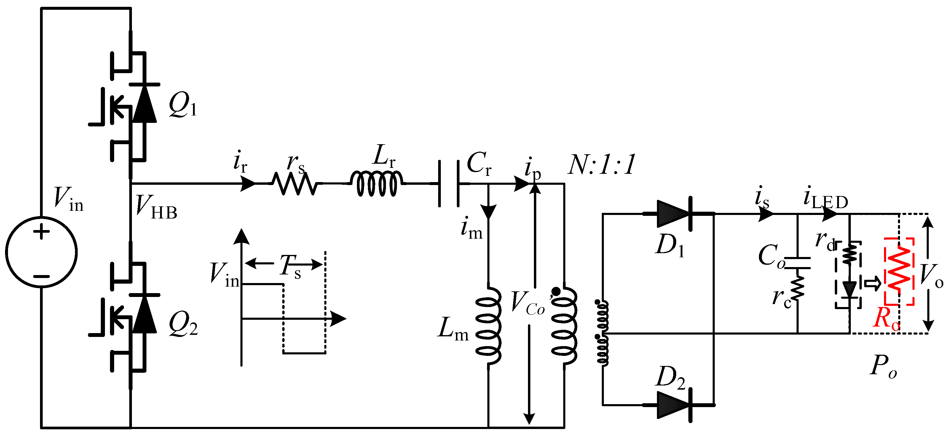
The typical circuit diagram of a half-bridge LLC LED driver is shown in
Figure 1, where voltage
Vab represents the half-bridge input quasi-square wave voltage and its peak voltage equals the input DC input voltage
Vin.
Lr and
Cr represent the resonant inductance and capacitance, respectively, and
rs is the parasitic resistance of the resonant loop.
Lm is the magnetizing inductance and the transfer ratio of the transformer is
N:1:1.
D1 and
D2 are rectifier diodes connected to the center-tapped secondary coil of the transformer.
Co is output filter capacitance and
rc is its parasitic resistance.
Vo and
rd represent output voltage and LED diode internal resistance, respectively.
ir,
im,
ip and
is are resonant current, magnetizing current, transformer primary side current and rectifier current, respectively.
Po is the nominal output power.
Ro is the output power equivalent load resistance, which will be used as the output load resistance in the following traditional EDF-based LLC LED driver small signal model. The main circuit parameter values are designed based on the FHA method and are given in
Table 1.
2.1. Traditional EDF-Based LLC LED Driving Small Signal Modeling
As has been pointed out in
Section 1, the analytical method to obtain a small signal model of the LLC converter is the EDF method. The deduction of the traditional EDF method can be divided into the following six steps.
2.1.1. Nonlinear Circuit Equations
The first step of the EDF method is listing the nonlinear equations of the LLC converter based on Kirchhoff voltage and current laws. In the traditional EDF modeling method, LED load is treated as an output power equivalent resistance
Ro which equals
Vo2/
Po. According to the half-bridge circuit diagram shown in
Figure 1, Equations (1)–(5) can be deduced.
where
The equivalent output voltage
VCo’ at the transformer’s primary side is
The relationship between the rectifier current
is and the output capacitance voltage
vCo is
According to (4), output voltage
vo can be represented as:
where
rc′ =
rc‖
Ro.
2.1.2. DC and First-Order Harmonic Approximation
In the second step, state variables are approximated by their fundamental sin and cos components. Resonant current
ir, magnetizing current
im and resonant capacitor voltage
vCr can be approximated by their fundamental harmonic as shown in Equations (6)–(8), respectively:
where
ωs is the switching angular frequency.
In Equations (6) and (7),
irs (
ims) and
irc (
imc) are the amplitudes of resonant current
ir (magnetizing current
im) fundamental sine and cosine components.
In Equation (8), Vin/2 is the DC bias component, and vcs and vcc are the amplitudes of resonant capacitance voltage vCr fundamental sine and cosine components.
2.1.3. Extended Description Function
The third step is the most important step because, in this step nonlinear variables in the circuit, equations are approximated by the DC and fundamental sin and cos components of state variables. The nonlinear terms in Equations (1) and (5) such as sgn(
ip)*
vCo’,
vab and
is can be approximated by their fundamental and DC terms as shown in Equations (9)–(11).
In Equation (9), the first-order harmonics amplitude
f1(d,
vdc) can be calculated by the Fourier series expansion method as given in Equation (12).
where
d is the duty ratio of half one switch cycle, and
vis is the first-order sine component of the resonant tank input voltage. The transformer’s primary voltage is also a triangle waveform with zero dc component, and its first-order harmonic is in phase with the primary winding current. By the EDF method, the sine and cosine components of the transformer’s primary voltage can be represented by Equations (13) and (14), respectively.
where
iss and
isc are the sine and cosine components of the transformer’s secondary current.
vps and
vpc are the sine and cosine components of the transformer’s primary voltage.
ips and
ipc are the sine and cosine components of the transformer primary current, and
ipp is the root mean square value of the transformer primary current first order harmonic sine and cosine amplitudes as in Equation (15).
2.1.4. Harmonic Balance Method
In the fourth step, by substituting the state variables and nonlinear variables into the nonlinear equations and adopting the harmonics balance method, the nonlinear large-signal model of the LLC converter can be deduced.
Substituting Equations (6)–(15) into Equations (1)–(5), the corresponding DC, sine and cosine terms are balanced, respectively. Thus, Equations (16)–(23) can be obtained.
2.1.5. Steady-State Working Point Calculation
Next, by assuming the deviation of state variables to be zero, the steady state working point can be calculated in the fifth step. Under the condition that the output power keeps constant, the output resistance
Ro can be transferred to the transformer’s primary side, and the equivalent resistance
Re is given in Equation (24).
According to Equation (22), Equation (25) can be calculated as:
Taking (25) into Equations (13) and (14), Equation (26) can be calculated:
According to KCL and harmonics balance, the relationship between sine and cosine components of resonant current
ir, magnetizing current
im and transformer primary current
ip is given in Equation (27).
When working in steady state, the state variables in Equations (16)–(23) do not change with time. By setting the time derivatives to be zero, the steady-state operation point can be calculated as shown in Equations (28)–(31). In (28), as
d is the duty ratio of half one switching cycle, the steady state value D equals one.
To calculate the steady state working point, it is better to represent Equations (24)–(31) in matrix form as shown in Equation (32).
where steady state variable vector
X = [
Irs,
Irc,
Vcs,
Vcc,
Ims,
Imc]
T, input variable vector
U = [
Vis, 0, 0, 0, 0, 0, 0]
T, and coefficient matrix E is given in Equation (33).
Then steady state working point can be calculated by matrix manipulation as in Equation (34).
2.1.6. Small Signal Perturbation
At last, based on the calculated steady-state working point, the small signal model of the LLC converter can be deduced by small signal perturbation nearby the steady-state working point.
To obtain the small signal model of the full bridge LLC converter, perturbation and linearization in Equation (34) should be taken at the steady state working point.
where
ωr is the resonant angular frequency, and
is the switching angular frequency perturbation normalized to
ωr.
By substituting Equation (35) into the large signal model of Equations (16)–(23) and eliminating the steady-state working point, the small signal model of the full bridge LLC converter can be obtained as follows:
where, coefficients
Hipc,
Hips,
Hvps,
Gipc, G
ips, G
vps,
Kips,
Kipc,
K1 and
K2 are defined in the equation below.
According to Equations (36)–(40), the state space small signal model of the full bridge LLC model can be deduced as shown in Equation (41).
where state variable vector
, input state variable vector
, output variable
, and coefficient matrix
A,
B and
C in Equation (41) are illustrated in Equations (42)–(44), respectively.
Based on Equation (41), the transfer function
of the half-bridge LLC converter is deduced in Equation (45).
where matrix
I is a unit matrix.
The traditional EDF-based LLC converter small signal model deducing method treats the load as a resistance Ro. After obtaining the transfer function
in Equation (45), the output current to normalized switching frequency transfer function
iLED/
fsN is calculated by Equation (46). For simplicity, this traditional EDF-based LLC LED driver small signal modeling method is denoted by
Req-
Ro.
However, the
Req-
Ro method has ignored the nonlinearity of LED load. There will be current flowing through the LED load once the positive bias voltage exceeds the threshold voltage
vth. Thus, to improve the accuracy of the transfer function
iLED/
fsN, Equation (47) should be adopted, where
rd is LED internal parasitic resistance. For simplicity, this improved EDF-based LLC LED driver small signal modeling method is denoted by
Req-
rd.
Comparing Equations (46) and (47), it can be seen that the gain calculated by (46) is not accurate. The larger the difference between Ro and rd is, the bigger the DC gain error calculated by Equation (46) is.
2.2. Improved EDF-Based LLC LED Driving Small Signal Modeling
Though Req-rd method has improved the DC gain accuracy of the calculated transfer function iLED/fsN. It is still based on the traditional Req-Ro method. The nonlinearity of LED load has not been taken into consideration during the deduction of the small signal model. To improve the accuracy of the transfer function iLED/fsN, the output power equivalent resistance load model should be replaced by the LED nonlinear model. For simplicity, this LED nonlinear model and EDF-based LLC LED driver small signal modeling method is denoted by iLED.
The first step is listing the nonlinear circuit equations. By simple circuit analysis, LED current
iLED can be calculated by Equation (48). The terminal voltage
vLED of LED is calculated by Equation (49), and the rectified current
is at the transformer secondary side is given in Equation (50).
where
rc′ =
rC//
rd.
Taking Equation (50) into Equation (49),
vLED can be deduced by Equation (51).
The second and third steps are the same as the traditional EDF modeling method, Equations (6)–(15) can be used here. In the fourth step, Equations (16)–(21) are the same as the traditional EDF modeling method too. While Equation (22) is replaced by Equation (52).
In the next fifth step, the steady state working state can be deduced. According to Equations (48) and (51), steady state Equations (53) and (54) are derived.
Taking (53) into Equations (16)–(21) and (52) and setting the deviation equaling zero, the steady state equations can be deduced as shown in Equations (55)–(57).
where
. According to Equations (55)–(57), the steady-state working points can be calculated by numerical calculation.
The last step is calculating the small signal transfer function by perturbation and linearization at the steady-state working point. The deduced state-space model of the LLC LED driver is given in Equation (58).
where state variable vector
, input state variable vector
, output variable
, and coefficient matrix
A1,
B1, C1 and
D1 in Equation (41) are illustrated in Equations (59)–(62), respectively.
Based on Equation (58), the transfer function
of the half-bridge LLC converter can be deduced from Equation (63).
where matrix
I is a unit matrix.
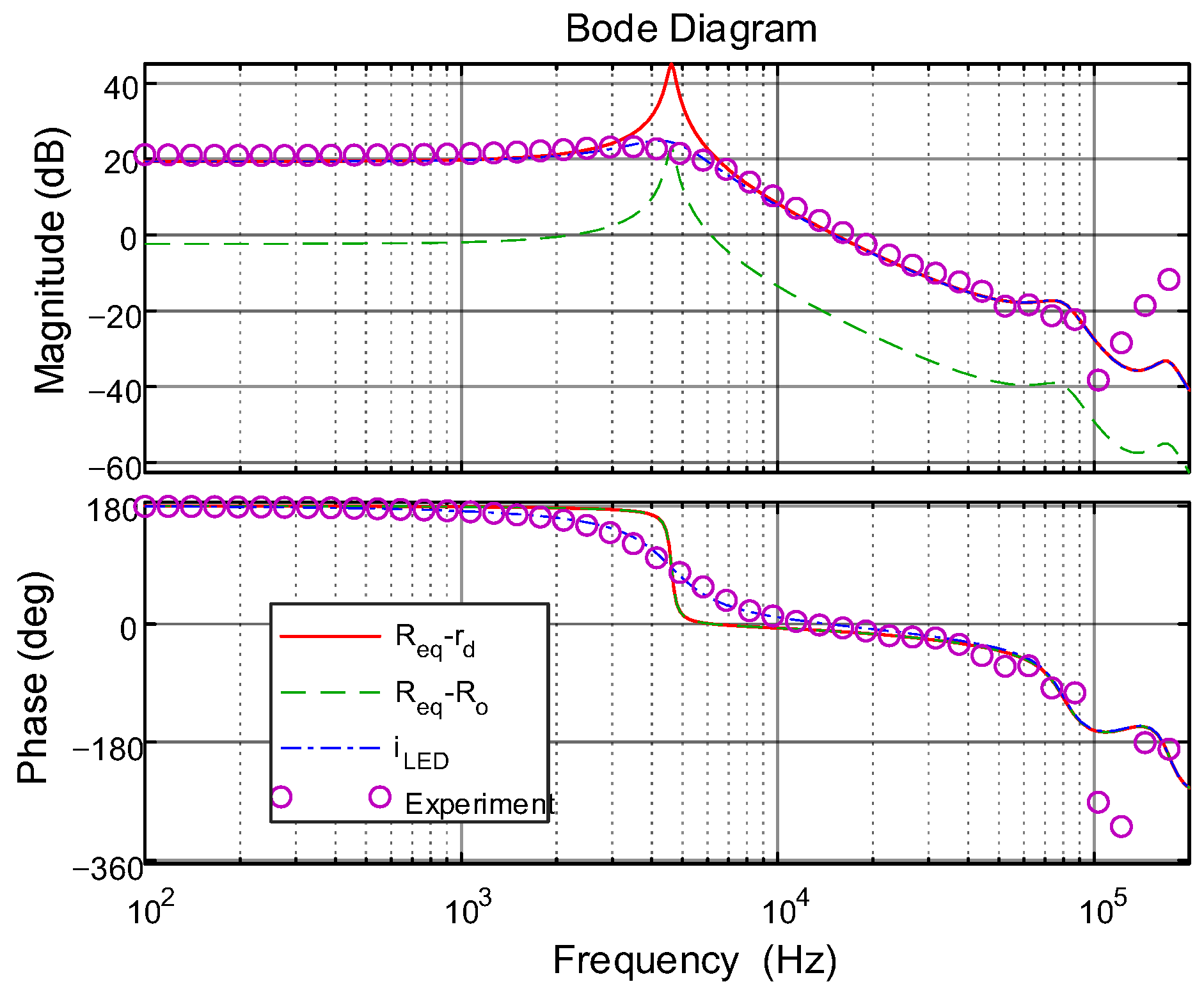
2.3. Small Signal Model Accuracy Verification
Based on the circuit parameters given in
Table 1, the bode diagrams of
Req-
Ro, Req-
rd and
iLED method-based transfer functions are illustrated in
Figure 2. In addition, a frequency sweep experiment is conducted in a circuit simulator to obtain the accurate transfer function
iLED/
fsN curve as shown in
Figure 2.
- (1)
The Bode diagram of the transfer function (TF)
iLED/
fsN (shown by the curve
iLED in
Figure 2) based on the LED nonlinear model is in consensus with that of frequency response experiment results (shown by the curve Experiment in
Figure 2), which verify that the small signal model based on the LED nonlinear model has the highest accuracy.
- (2)
As in paper [
3,
4] and shown in
Figure 2, TF
iLED/
fsN calculated by
vo/
fsN/
Ro (Bode diagram shown by the curve
Req-
Ro in
Figure 2) causes the calculated open-loop gain much less than that of LED nonlinear model-based calculated TF. While the open-loop gain of the TF calculated by
vo/
fsN/
rd (Bode diagram shown by the curve
Req-
rd in
Figure 2) is almost the same as that of LED nonlinear model based calculated TF as illustrated in
Figure 2. This is because the threshold voltage of lighting LED is large and the power equivalent resistance
Ro of LED is much greater than its internal resistance
rd. Thus, after obtaining TF
vo/
fsN between the output voltage
vo and the normalized switching frequency
fsN based on the power equivalent resistance model of LED, the TF
iLED/
fsN should be calculated by
vo/
fsN/
rd, not
vo/
fsN/
Ro.
- (3)
As it has been verified that the calculated circuit DC working points are almost the same regardless of if the LED nonlinear model or the power equivalent resistance model is taken into account. In fact, the main difference between the LED nonlinear model and power equivalent resistance-based LLC converter small signal model comes from the load model itself. From
Figure 2, it can be seen that the small internal resistance of LED has a significant impact on the damp ratio of the oscillation element with a pair of dominant complex poles in the TF
iLED/
fsN. The closer the internal resistance
rd is to the power equivalent resistance
Ro, the more accurate the power equivalent resistance
Ro based small signal model is.
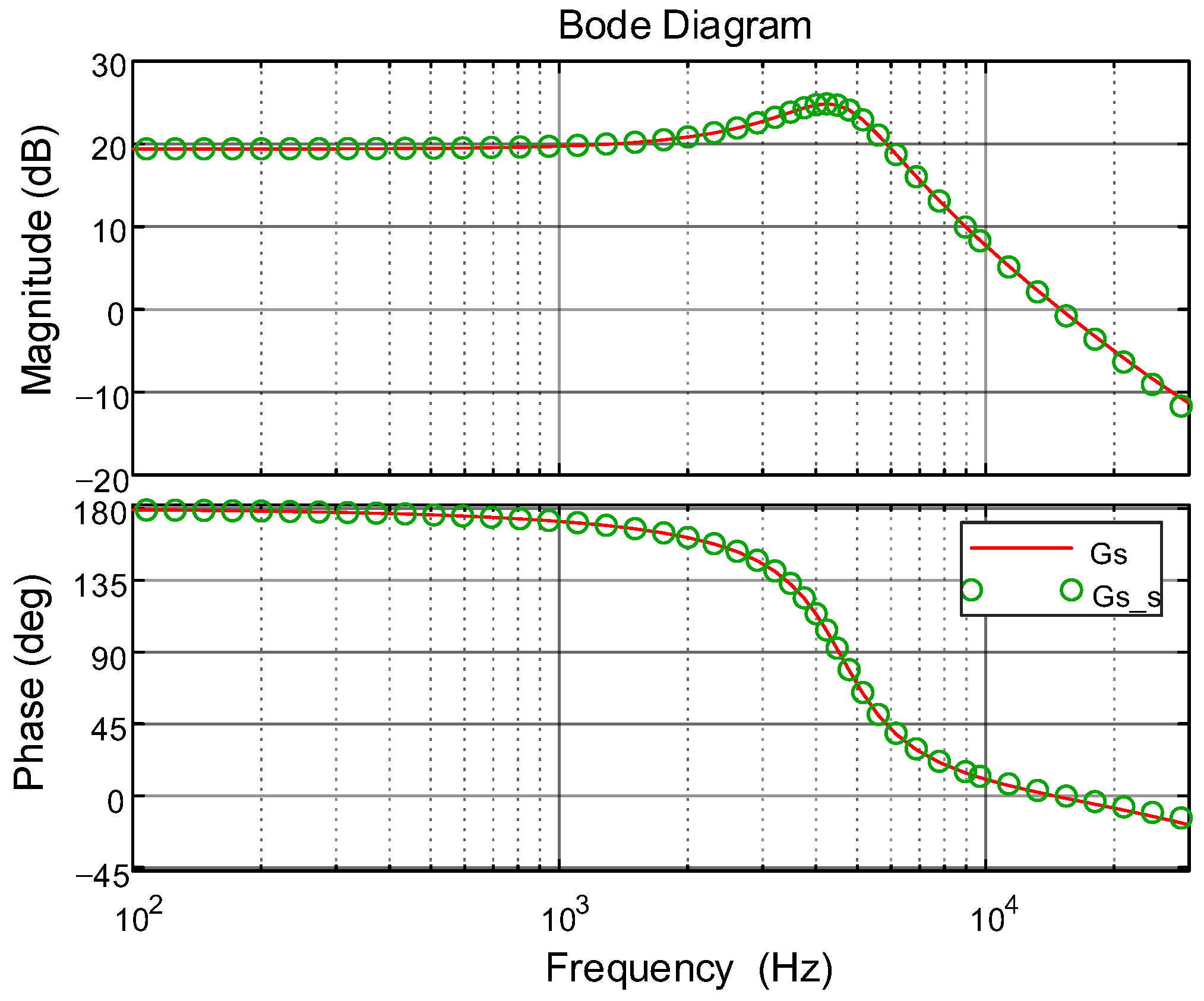
Based on the circuit parameters given in
Table 1, the LED nonlinear model-based TF
iLED/
fsN is deduced as given in Equation (64).
Equation (64) is too complex for the design of a compensation controller. Thus, it can be simplified by dominant poles and right half plane (RHP) zero as in Equation (65). Though simplified, the accuracy of the open-loop TF is reserved as illustrated in
Figure 3.
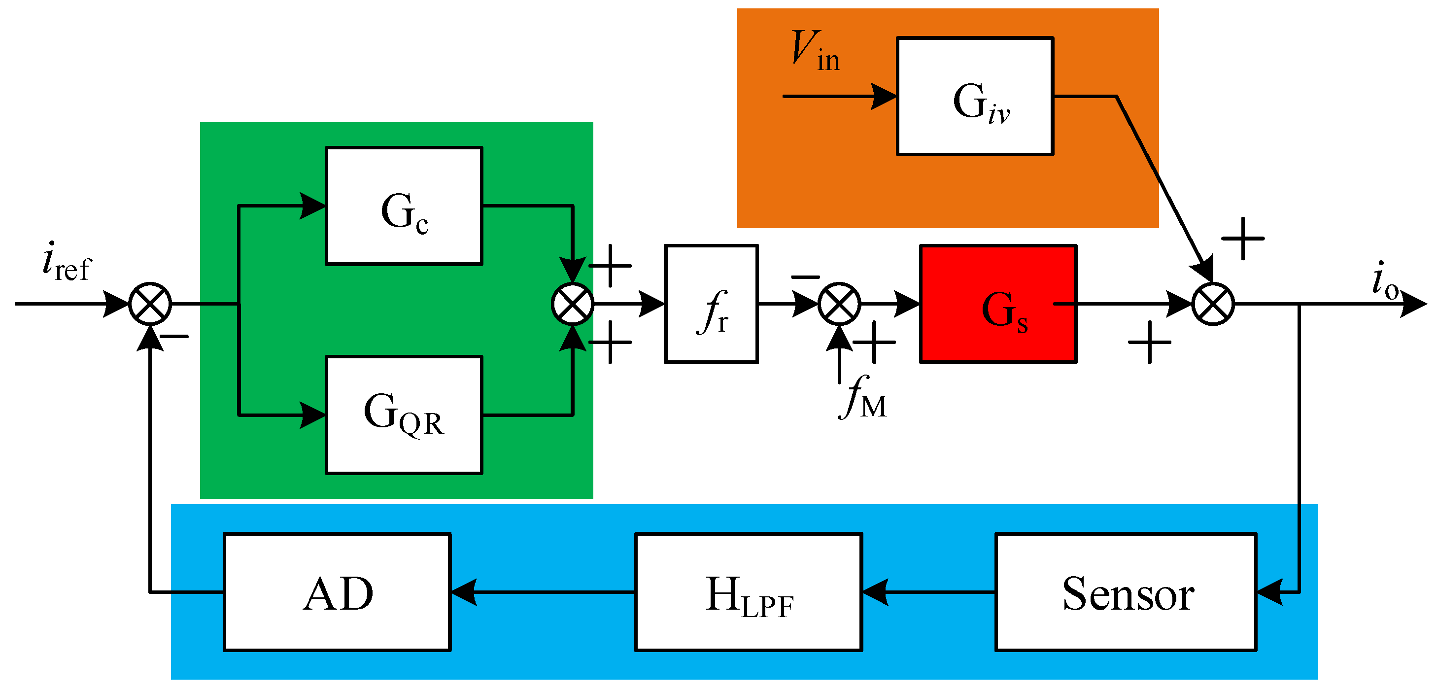
3. Close-Loop Control of LLC Converter with LED Load
The close-loop control diagram of the LLC LED driving converter is illustrated in
Figure 4. As has deduced the output current to normalized switching frequency open-loop TF
Gs, the compensation controller
Gc can be designed with the desired steady state and dynamic performance obtained. However, in order to promote the reliability and duration of the LLC LED driver, the input large capacitance value electrolytic capacitor has been replaced by a small capacitance value film capacitor, which causes that there is alternate current (AC) voltage ripple in the input DC voltage. As the input DC voltage comes from the front-end rectifier, the frequency of the input AC ripple voltage is two times that of grid voltage
fac. The input AC voltage ripple will cause considerable output current ripple, so the active ripple rejection (ARR) method must be adopted.
In order to suppress the input AC voltage-caused output current ripple, a high-gain quasi-resonant controller (QRC)
GQR at the frequency of 2
fac is adopted. As shown in
Figure 4, the QRC is in parallel with the controller
Qc. Controller
Qc takes the role of the average output current regulation and the QRC has a significant effect on the output current ripple rejection.
3.1. Quasi-Resonant Controller-Based ARR
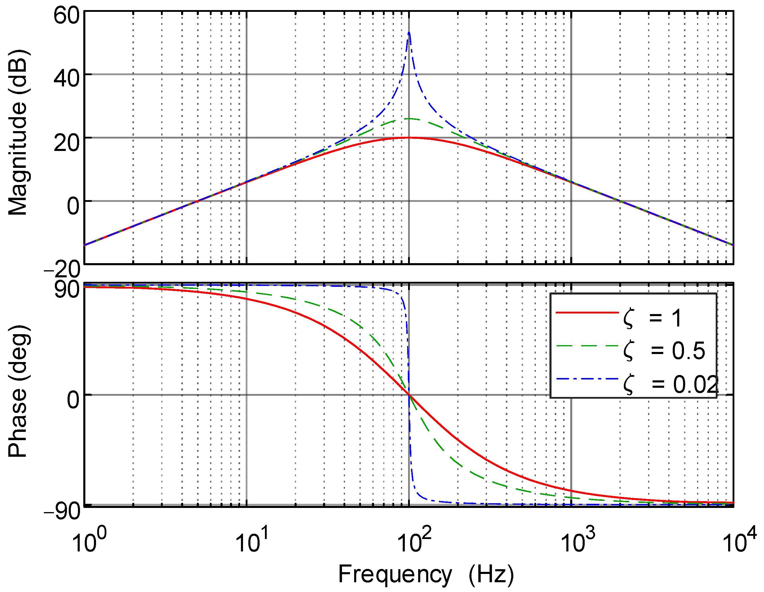
The TF of the QRC is given in Equation (66), in which there are gain
k, center angular frequency
ωo and damping ratio ζ as the three control parameters. Setting the center frequency to be 2
fac (100 Hz), the Bode diagrams of the QRC under different damping ratios ζ are shown in
Figure 5.
From
Figure 5, the following can be seen:
- (1)
The QRC has an adjustable peak amplitude at the center angular frequency ωo. So, the center angular frequency ωo of the QRC can be set to be two times the grid voltage frequency to obtain a maximal gain of the input signal.
- (2)
The value of the damping ratio has an important influence on the amplitude and passband of the QRC. The smaller the damping ratio is, the larger the peak gain and the narrower the passband. So, the value of the damping ratio should be designed under the balance of peak gain and the passband width.
- (3)
Control parameter gain k can promote the gain at the whole frequency range, which is not recommended to be set too large to simplify the design of the compensation controller Qc.
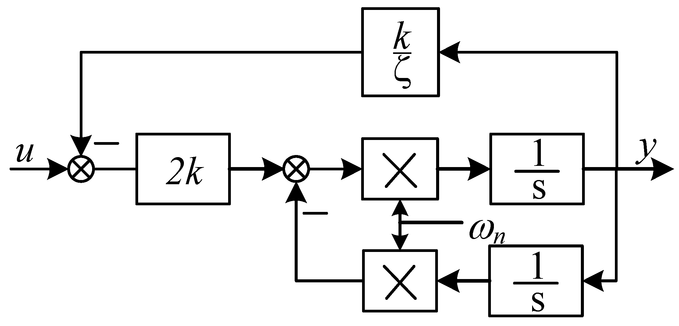
The control diagram of the QRC is illustrated in
Figure 6.
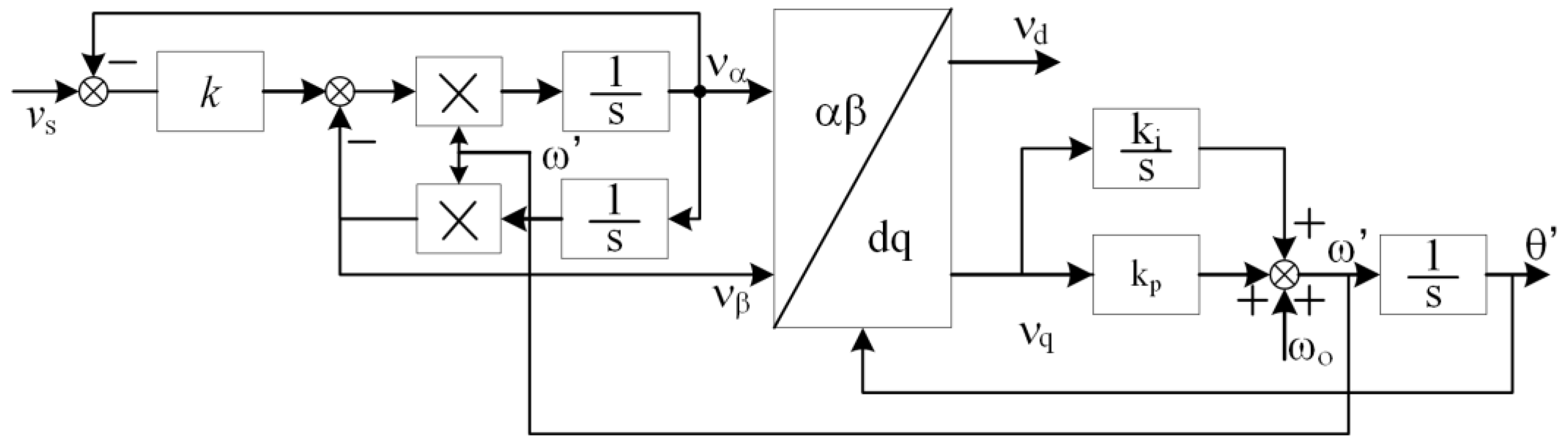
If the frequency of the grid voltage is stable, a small damping ratio value can be chosen to have a large enough gain with good output current ripple rejection performance guaranteed. However, in practice, the grid voltage frequency is varying because of the dynamic changing of source and load power. To obtain a good ARR performance, a second-order general integral (SOGI) single-phase SPLL as shown in
Figure 7 is adopted to trace the grid frequency.
By dynamically changing the center frequency of the QRC according to two times of the SPLL locked grid frequency, the output current ripple can be suppressed to a considerably small level.
3.2. Compensation Controller Design
Now it comes to the design of the compensation controller
Gc. The design of controller
Gc is based on the deduced simplified open-loop TF given in (2). As can be seen that the system type of (2) should be promoted to be one to eliminate the steady-state error. So, compensator
Gc should have an integral element. At the same time, the two dominant poles in (2) will cause too large a declining speed of logarithmic amplitude and phase curves, which is not favorable to stability and dynamic response performance. Thus, two zeros same as that of the dominant poles are added in the compensator
Gc. In addition, to suppress the gain at frequency points no less than the switching frequency, a pole at half of the switching frequency is added to
Gc. Based on the above compensator design principle, the TF of the controller
Gc is given in Equation (67).
In Equation (67), kc is the open-loop gain and ωs is the minimal switching angular frequency. Open loop gain kc of Gc is designed according to the desired phase margin and amplitude crossover frequency ωc.
As shown in the close-loop control diagram in
Figure 4, to filter out the switching frequency noise, there is a second-order low pass filter (LPF) in the feedback loop and its TF G
LPF is given in Equation (68).
In (68), ωf is the cut-off frequency of the LPF and Q is the quality factor. In the design of the LPF, ωf is set to be 20 kHz, which is less than half of the analog-to-digital conversion (ADC) sampling frequency to filter out the high-frequency noise and Q is set to be 0.5 to obtain a smooth filtering performance.
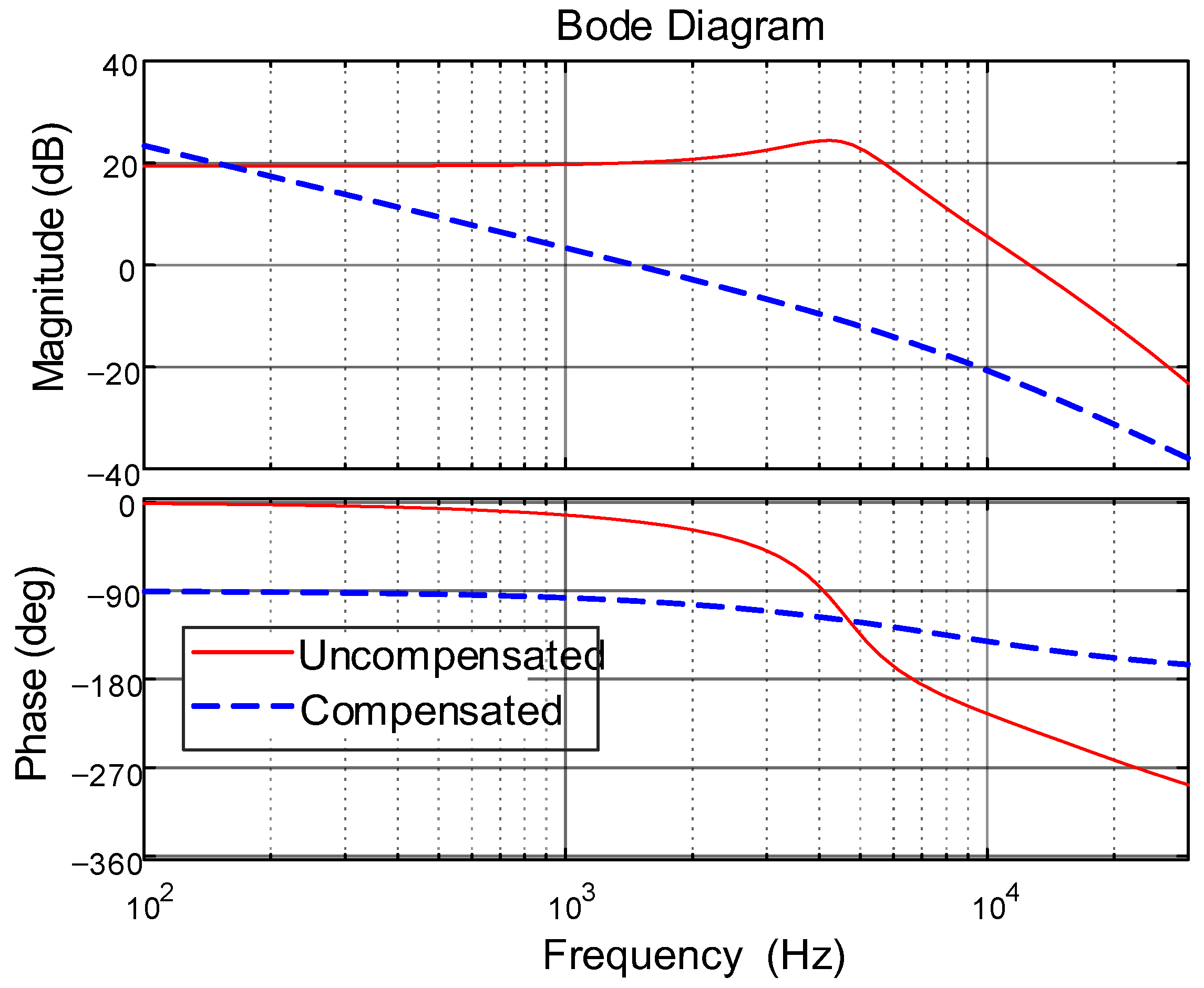
By far, the loop gain
Gall of the LLC LED driving converter can be obtained by multiplying the three TFs shown in Equations (65), (67) and (68). In practical control, the AD sampling frequency is 50 kHz, and the switching frequency equals the resonant frequency of 100 kHz. The Bode diagrams of both TF in Equation (65) and
Gall are illustrated in
Figure 8.
From
Figure 8, it can be seen that without a compensator, the original control system is unstable. Under the designed compensator, the crossover frequency of the compensated control system is set to be 1.46 kHz with a phase margin of 79.6°. The open-loop gain
kc of the compensator
Gc is set to be 1000.
4. Simulation Verification
To verify the correctness and effectiveness of the constructed LLC LED driving converter small signal model, the QRC controller, the SPLL-based output current ripple method and compensation controller design method, the LLC LED driving converter as shown in
Figure 1 simulating prototype is constructed in Simulink and the close-loop controller shown in
Figure 4 is implemented in the simulation experiment. In the simulation, the input DC voltage Vin is 400 V, and the default input AC voltage is a sine wave with a peak voltage of 40 V and frequency 100 Hz. The control parameters damping ratio and gain of the QRC controller are set to be 0.02 and 1, respectively.
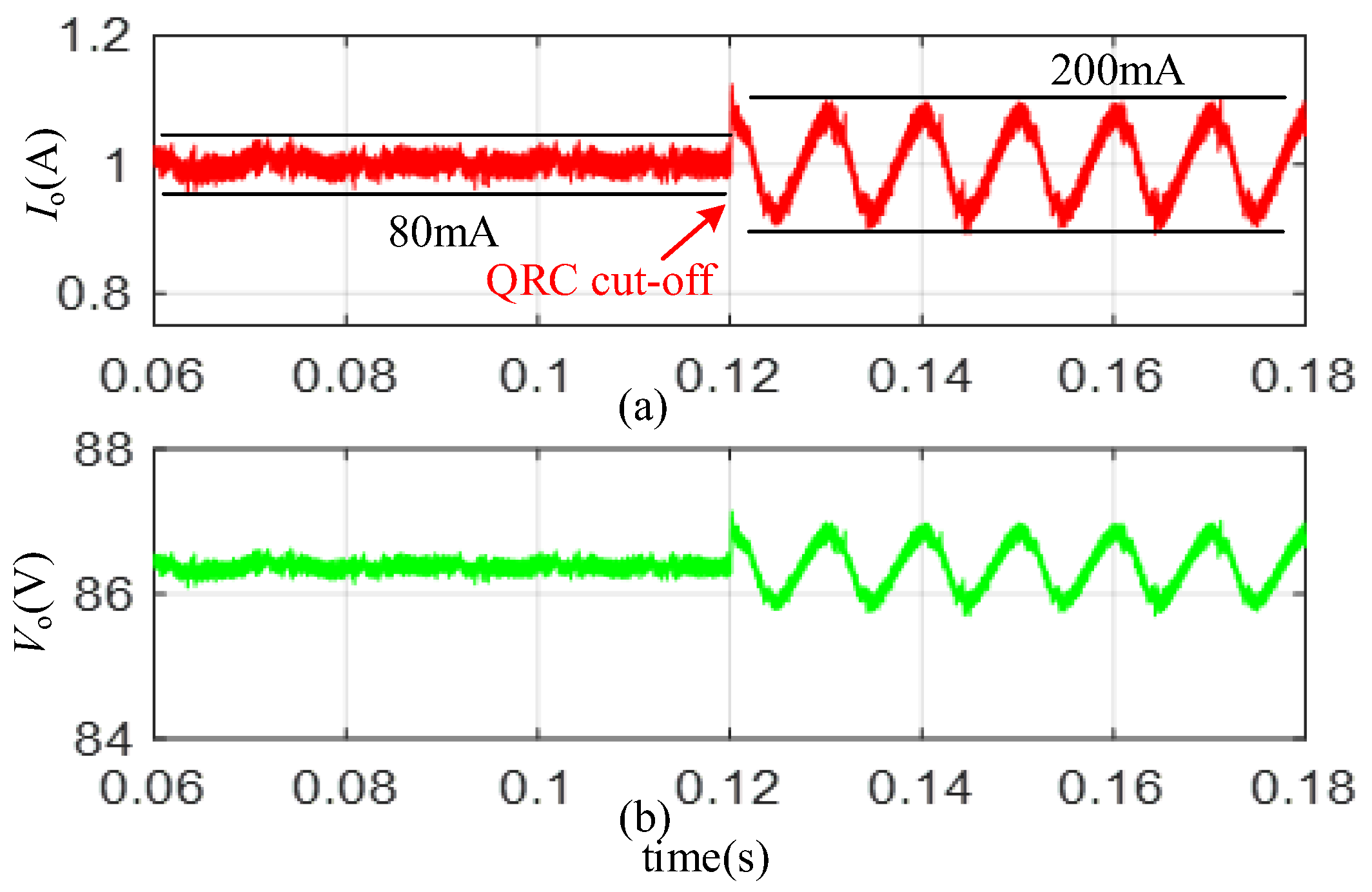
Figure 9 illustrated the output current and voltage waveform under the control of the proposed compensation controller with and without the QRC. Before time 0.12 s, both compensator
Qc and output current ripple rejection controller QRC work, and the output current is controlled to the reference value 1 A with a peak-to-peak current ripple of 80 mA. After 0.12 s, the QRC controller is cut-off and the peak-to-peak output current ripple is increased to 200 mA.
Figure 9 has verified the correctness and effectiveness of the compensation controller and output current ripple rejection controller QRC.
In
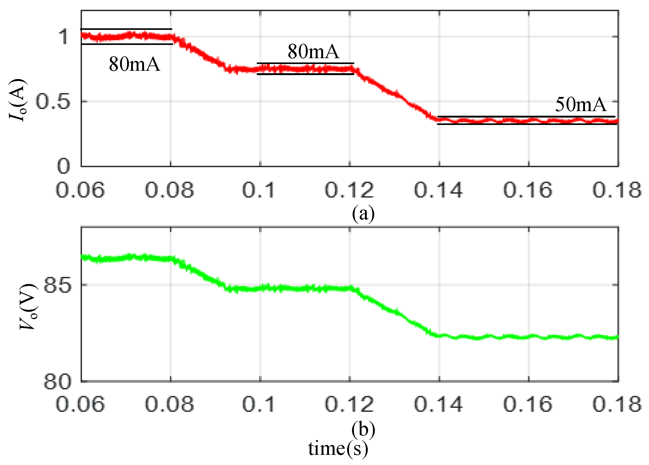
Figure 10, the LLC LED driving converter is controlled with the designed compensator
Qc and ARR controller QRC, and the dynamic output current and voltage are illustrated under dimming conditions. Before 0.08 s, the reference current is 1 A. In the time span from 0.08 to 0.09, the reference current declined linearly from 1 A to 0.75 A. In the time span from 0.09 to 0.12, the reference current keeps being 0.75 A. After that, in the time span from 0.12 to 0.14, the reference current decrease linearly from 0.75 A to 0.35 A once again and stays at 0.35 A.
From
Figure 10, it can be seen that the close-loop controller can closely follow the changing reference current without overshooting.
Figure 10 has further verified that the designed compensator and ARR controller can effectively control the output average current and suppress the output current ripple under different current levels and have good dynamic performance.
In
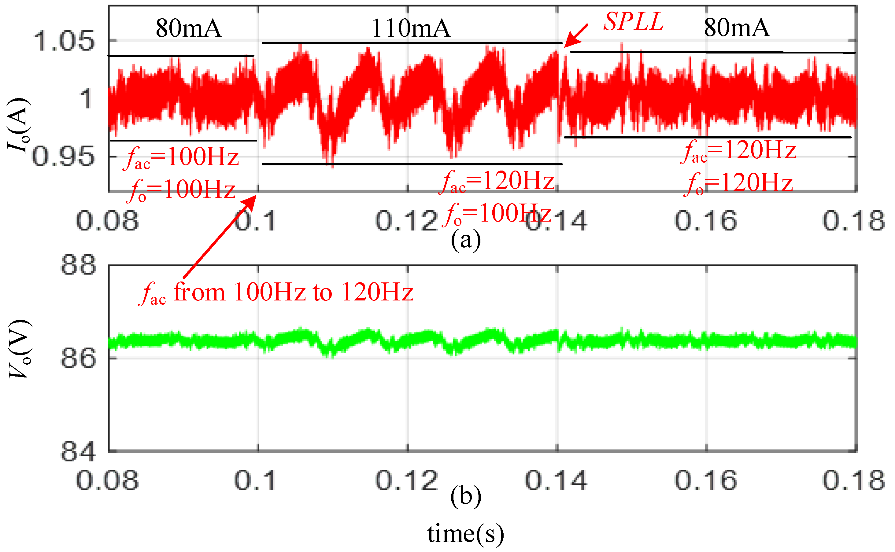
Figure 11, before time 0.1 s, the input AC voltage frequency is 100 Hz, while after 0.1 s, the input AC voltage frequency is jumped to 120 Hz. In the time span from 0.1 s to 0.14 s, the center frequency of the QRC controller still keeps 100 Hz, and the output peak-to-peak current ripple is increased from 80 mA to 110 mA because of the gain decreasing of the QRC when the input voltage frequency deviating from the QRC center frequency. Compared with the 200 mA peak-to-peak current ripple shown in
Figure 9, it can be seen that the QRC can still suppress the output current ripple at the nearby of its center frequency. After 0.14 s, the center frequency of the QRC is updated to be 120 Hz based on the SPLL locked grid frequency. It can be seen that the output peak-to-peak current ripple is decreased from 110 mA to 80 mA again.
Figure 11 has verified that the SPLL-based QRC can effectively suppress the output current ripple even if the grid voltage frequency deviates from the nominal value, which makes it suitable for the weak power grid with large amounts of new energy penetration.


