
Review: Heterojunction Tandem Solar Cells on Si-Based Metal Oxides
 ,
,
Abstract
:
1. Introduction
2. Fabrication Techniques and Device Architecture
2.1. Basics on Tandem Devices
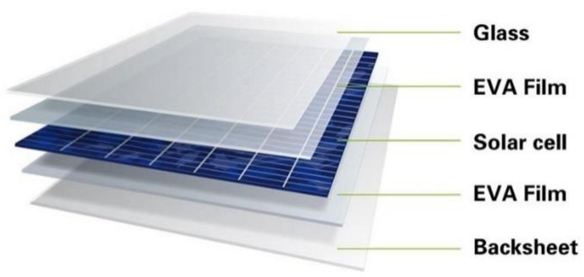
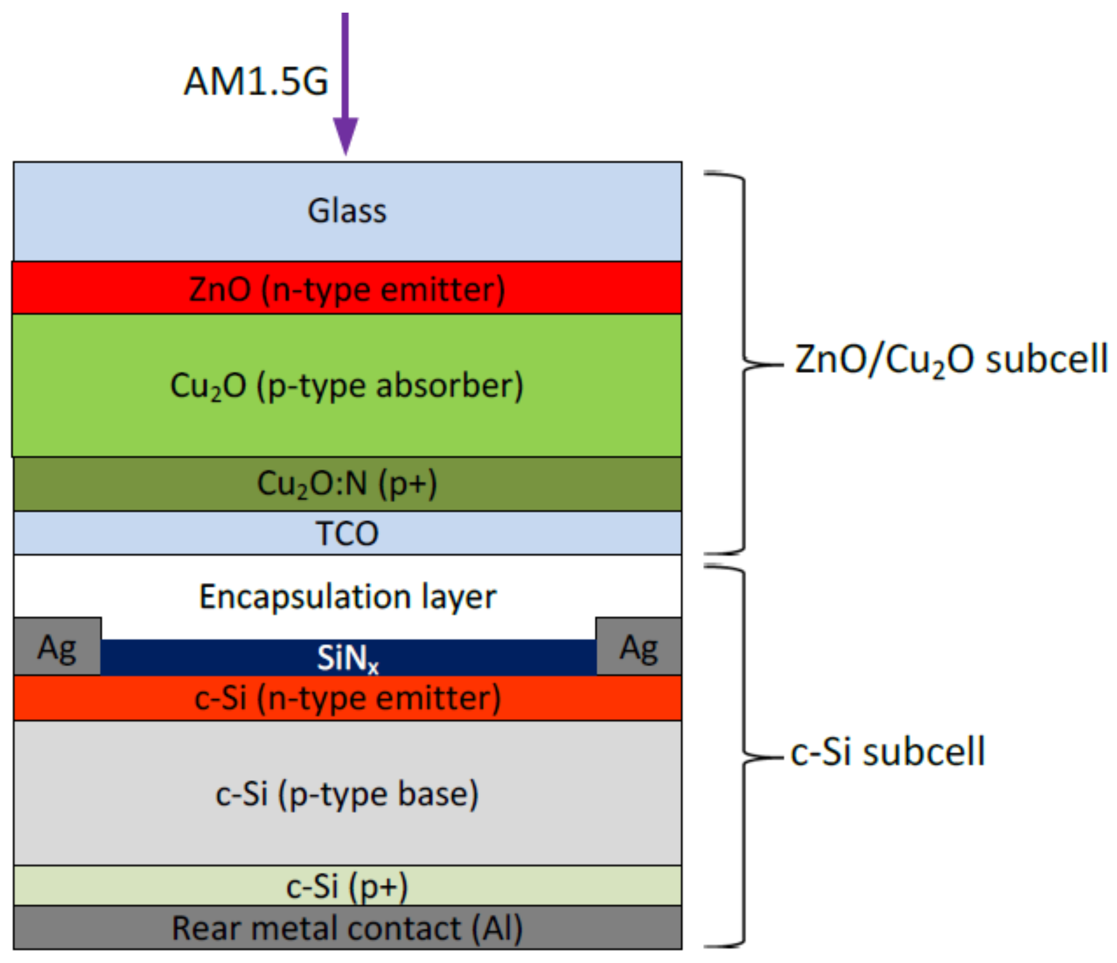
2.2. Device Architecture
2.3. Cu2O Fabrication Techniques
- A.
- Pulsed Laser Deposition (PLD) [37]
- B.
- Magnetron Sputtering (MSP) [38]
- C.
- Metal Organic Chemical Vapor Deposition (MOCVD) [39]
- D.
- Plasma-enhanced Atomic Layer Deposition (ALD) [40]
2.4. ZnO Fabrication Techniques
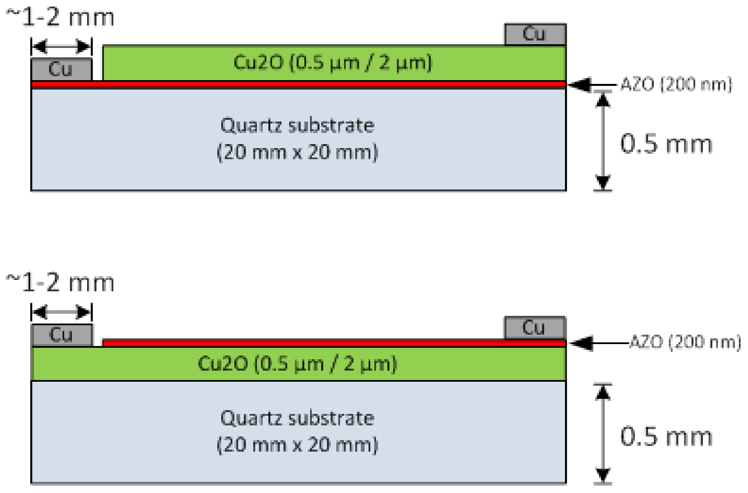
2.5. Fabrication of Cu2O/ZnO Heterojunction
3. Characterization of Cu2O and ZnO Layer Structures
3.1. Characterization of Cu2O Layer Structure
3.1.1. Basic Information
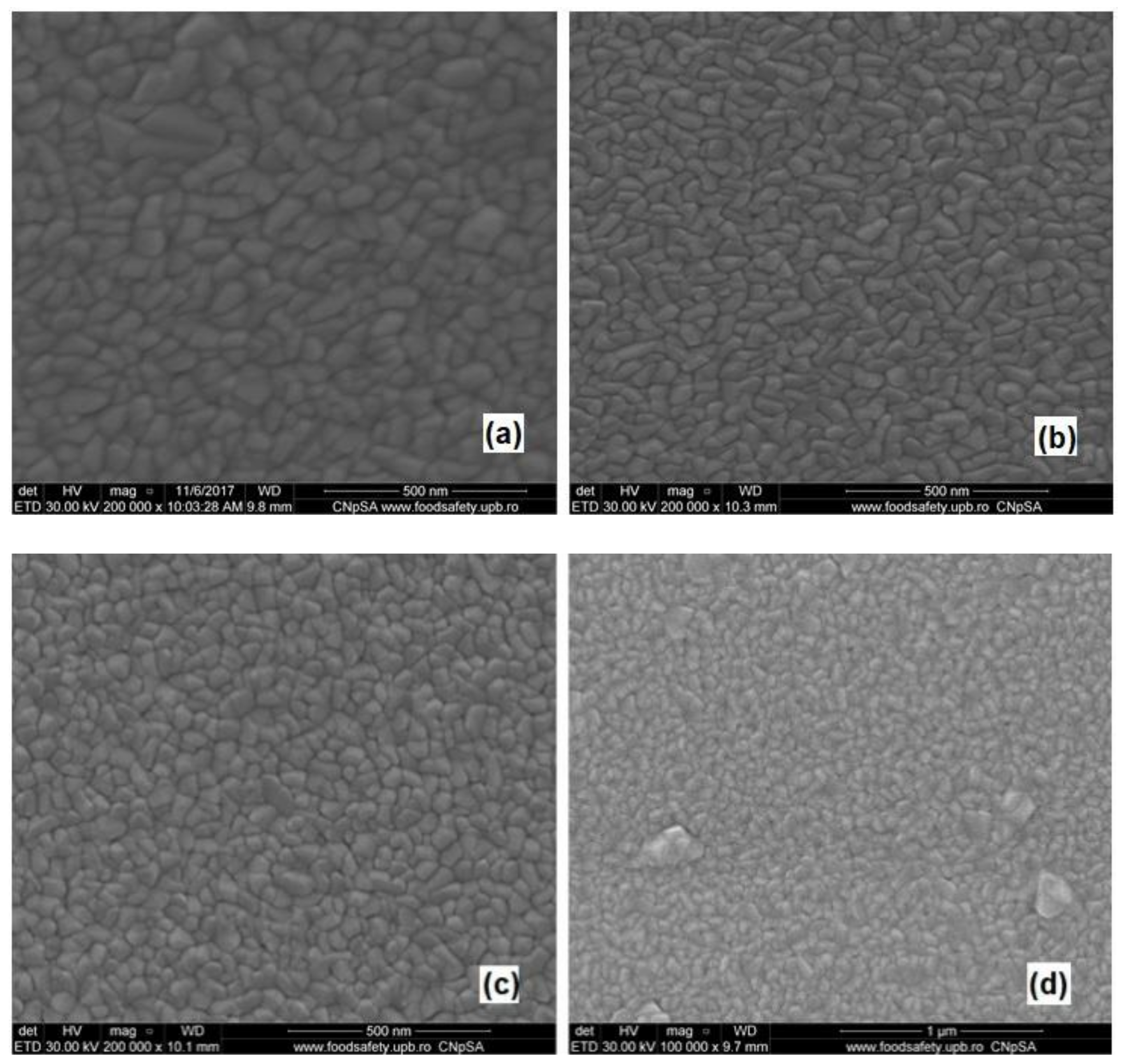
3.1.2. Morphological Characterization of the Cu2O: N Thin Films
- A.
- Scanning Electron Microscopy (SEM)
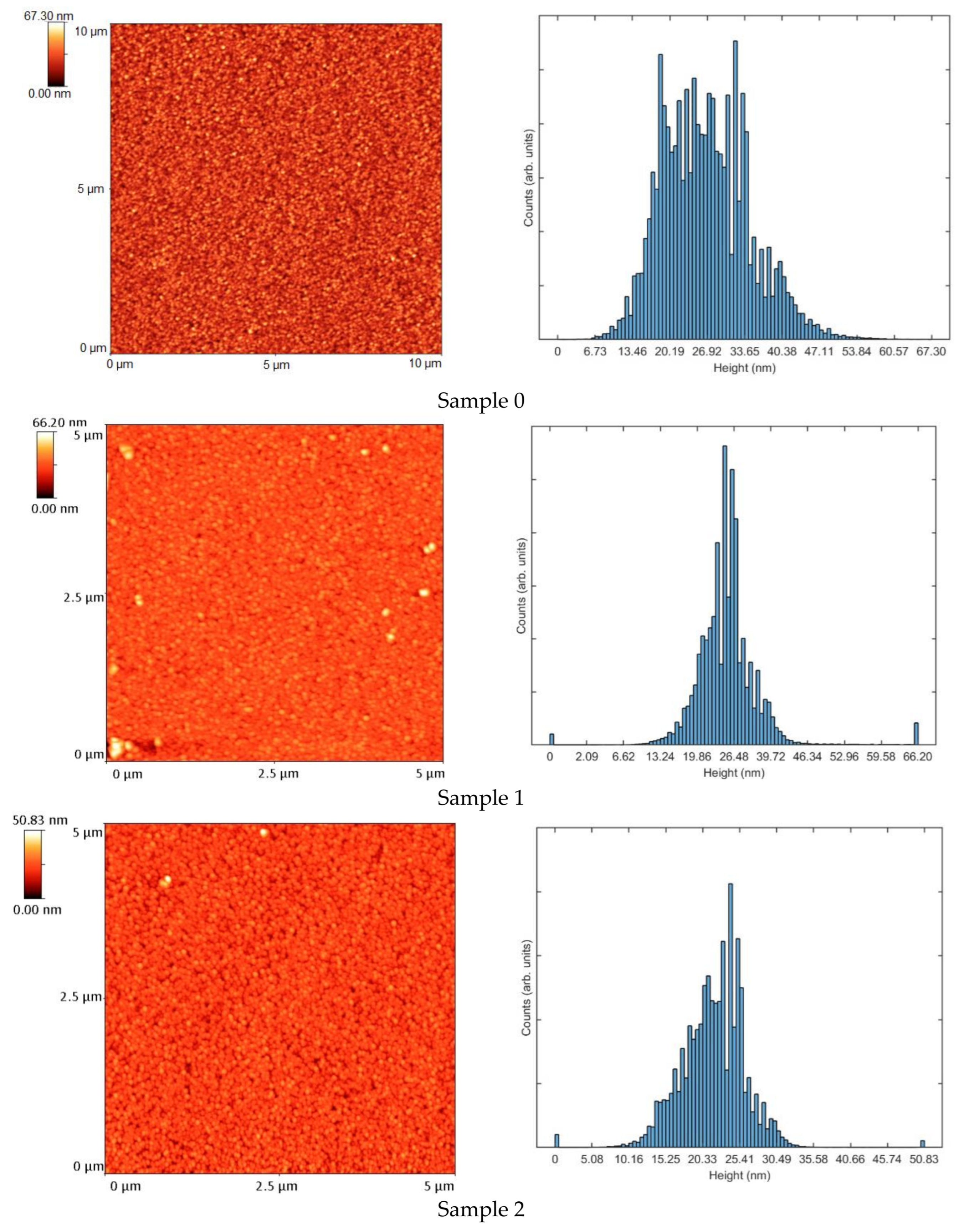
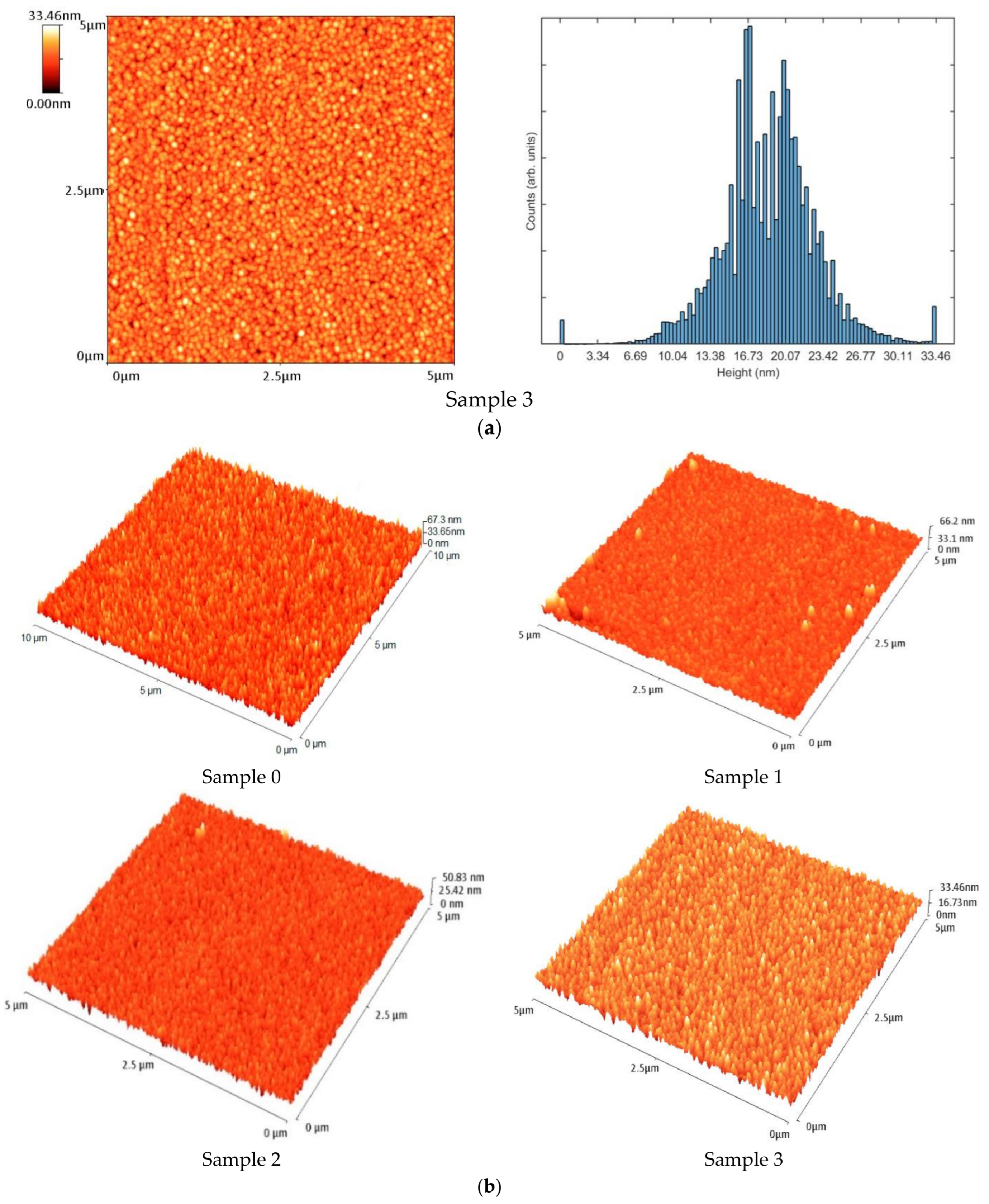
- B.
- Atomic Force Microscopy (AFM)
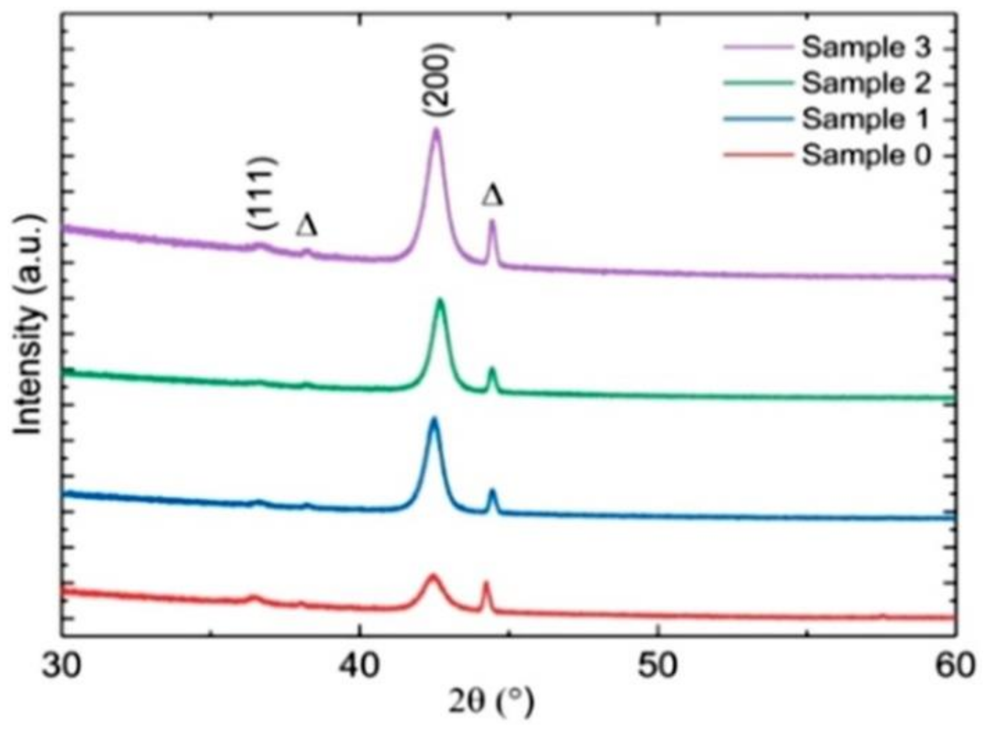
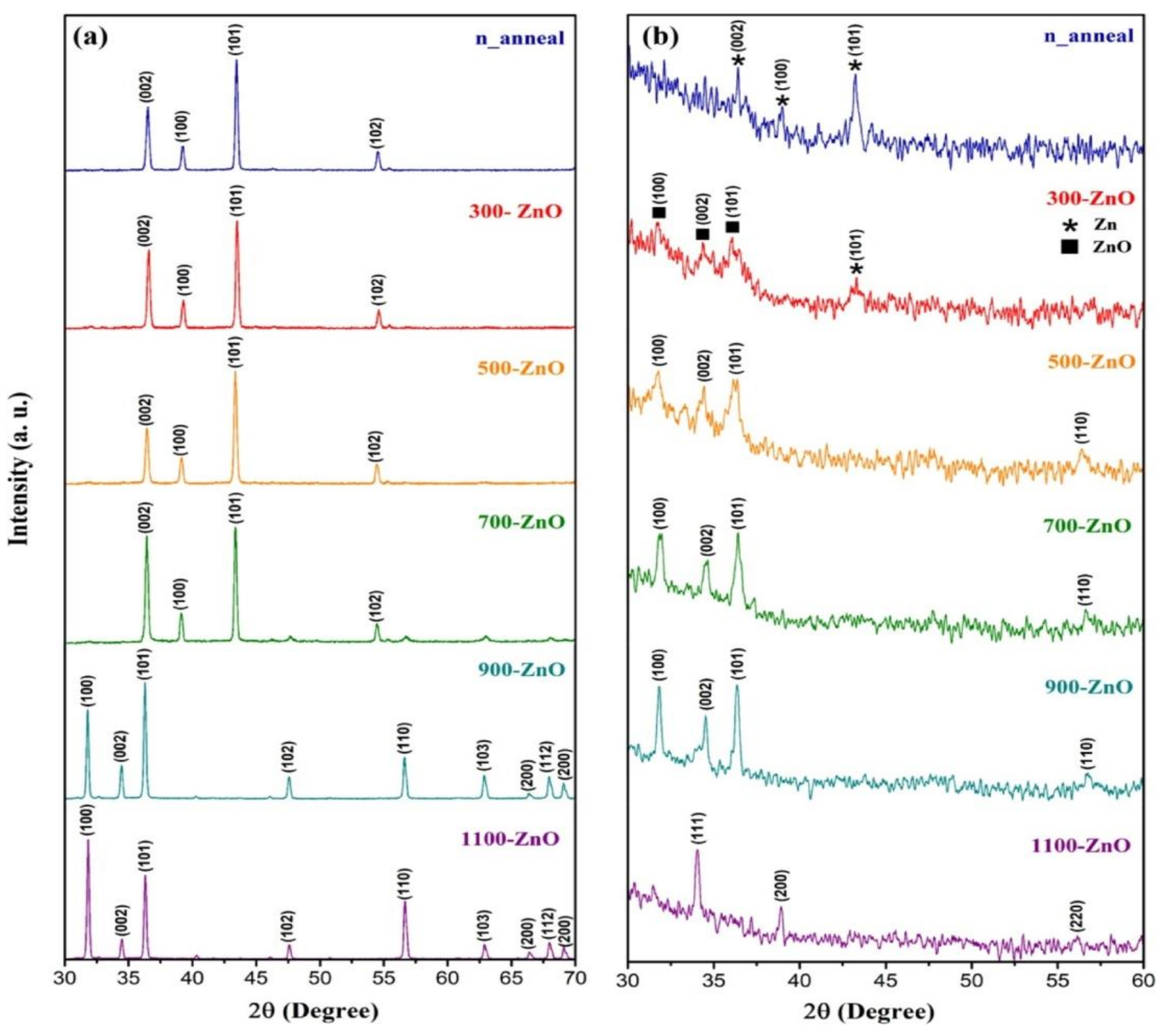
3.1.3. Structural Characterization by XRD of the Cu2O:N Thin Films
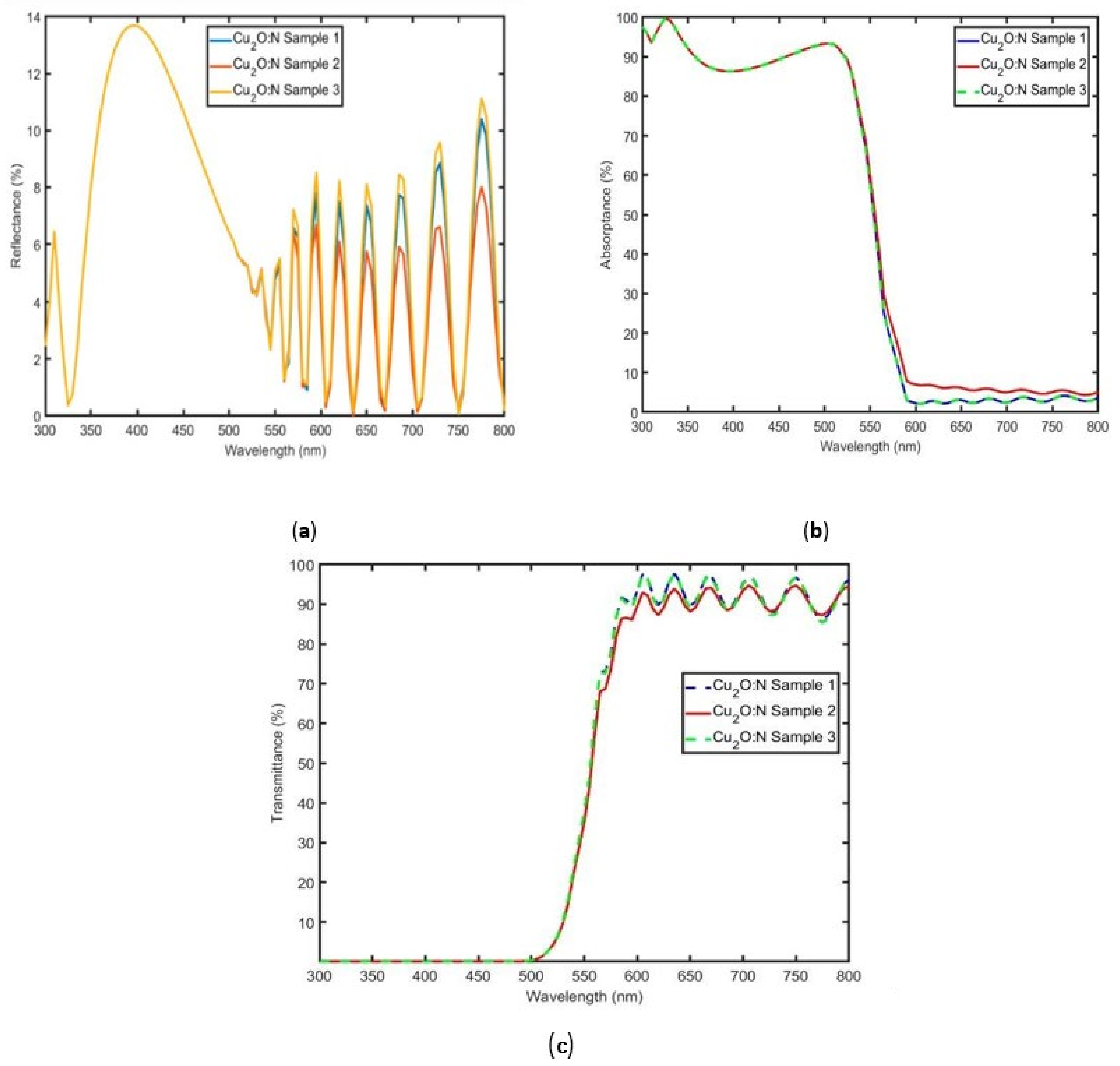
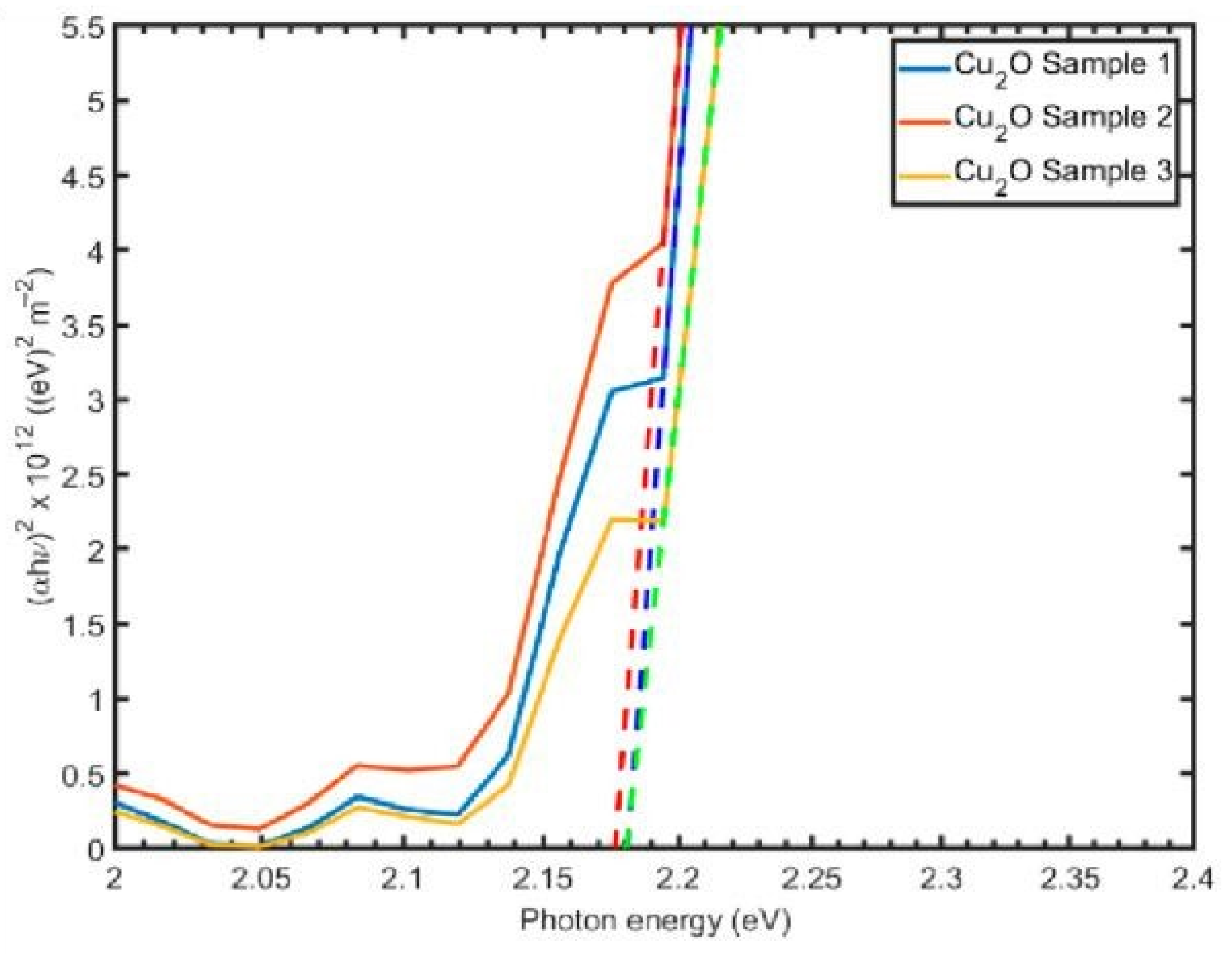
3.1.4. Optical Characterization of the Cu2O:N Thin Films
- A.
- FTIR Spectroscopy characterization.
- B.
- Spectroscopic Ellipsometry (SE) Characterization
3.2. Characterization of ZnO Layer Structure
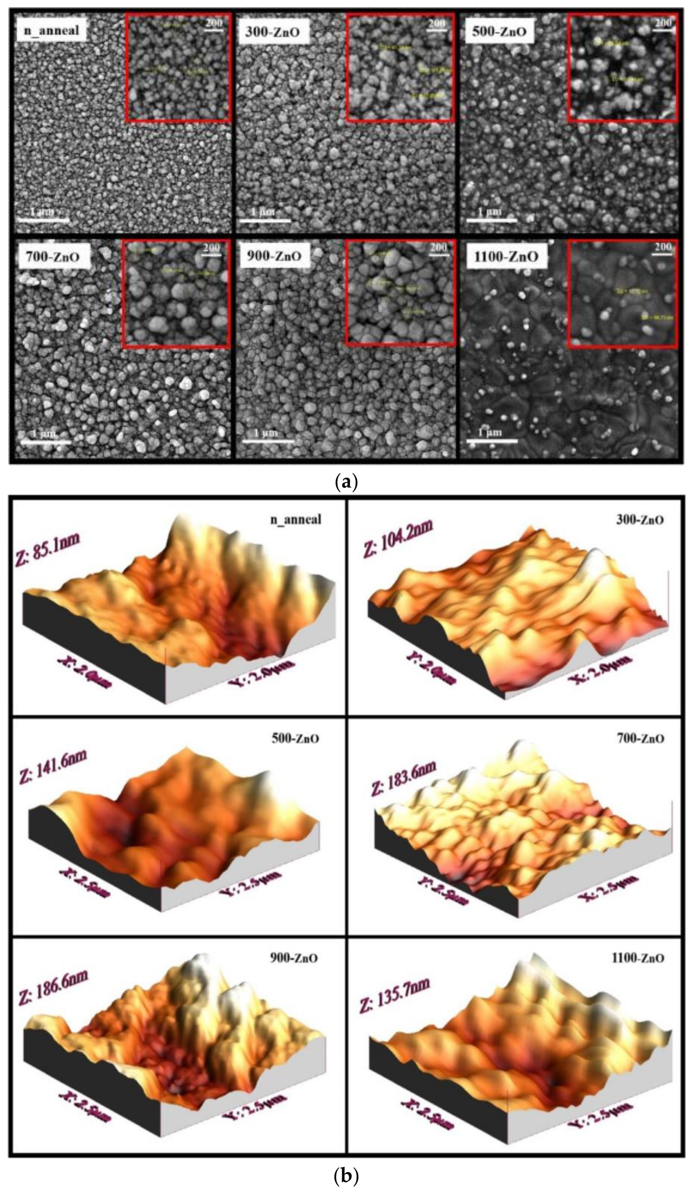
3.2.1. The Structural Properties of ZnO Nanostructures
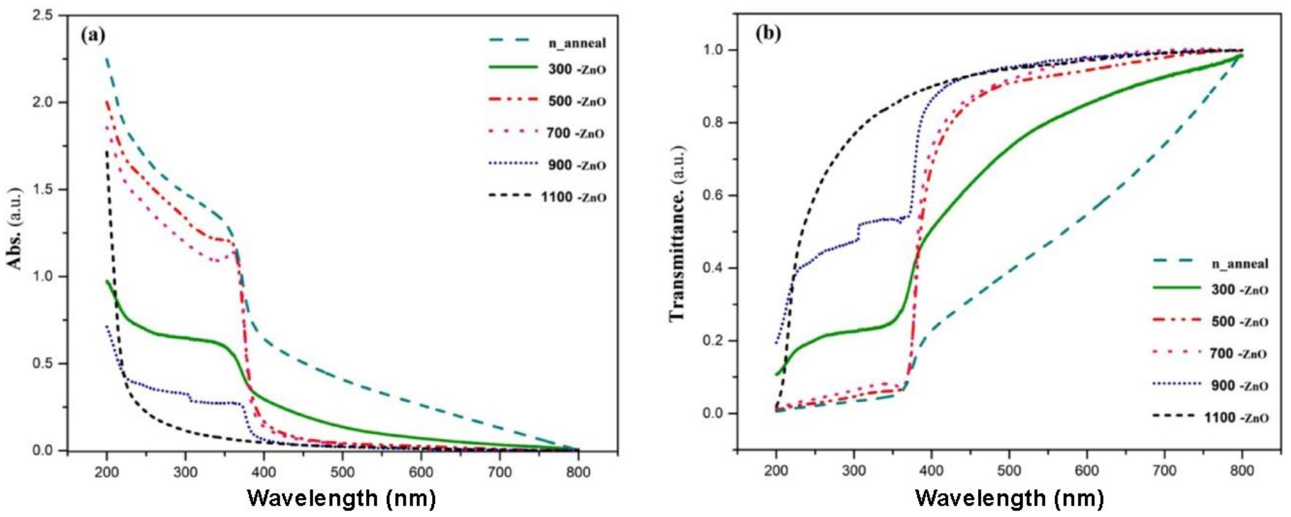
3.2.2. Optical Properties of ZnO Thin Films
- A.
- UV-VIS Spectroscopy
- B.
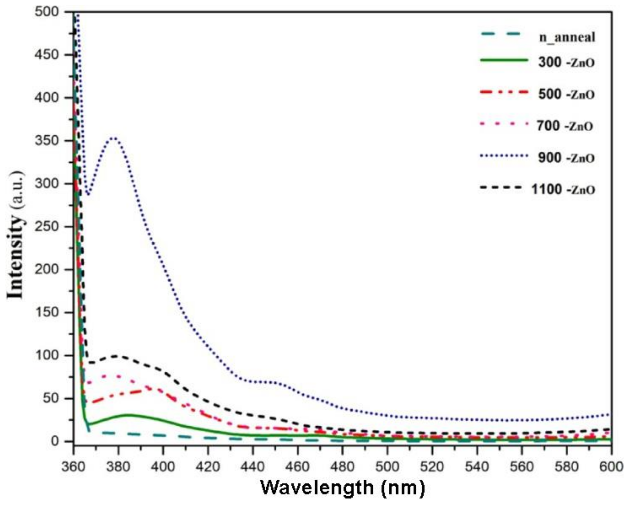
- Photoluminescence (PL) Spectroscopy
- C.
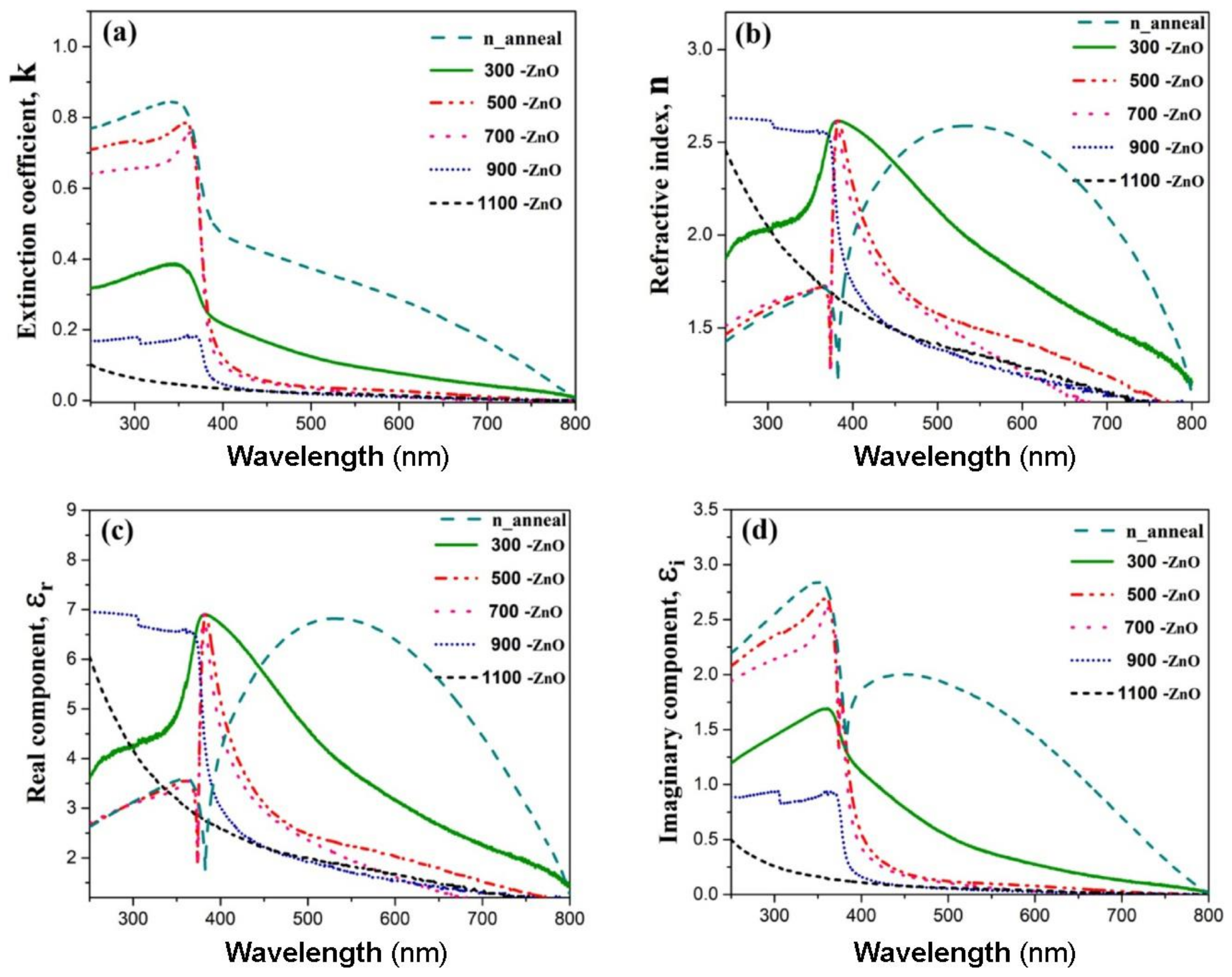
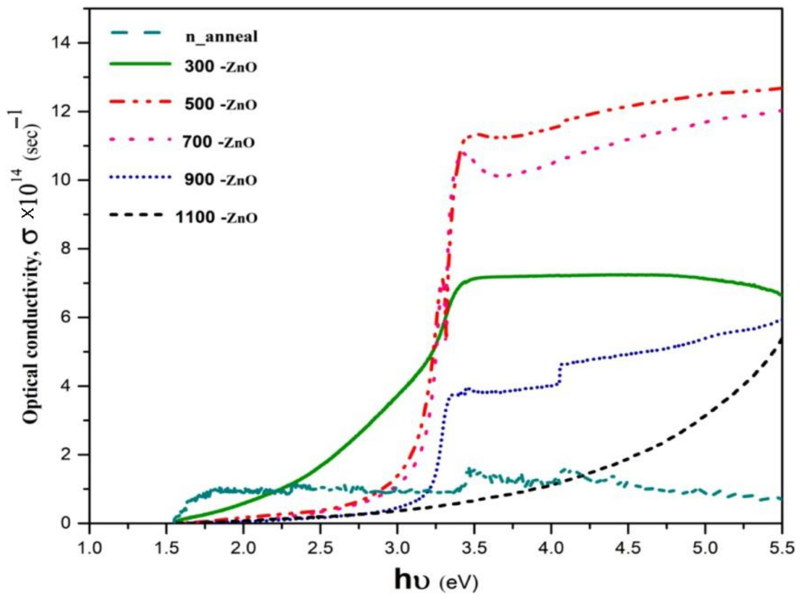
- Determination of Optical Constants
4. Merits and Comparative Analysis of AZO/Cu2O HTSC
4.1. Merits of AZO/Cu2O Heterojunction Tandem Solar Cells (HTSC)
4.2. Comparative Analysis of HTSC with Other High Performance Solar Cells
5. Numerical Modelling of Heterojunction Tandem Cu2O/ZnO Solar Cells
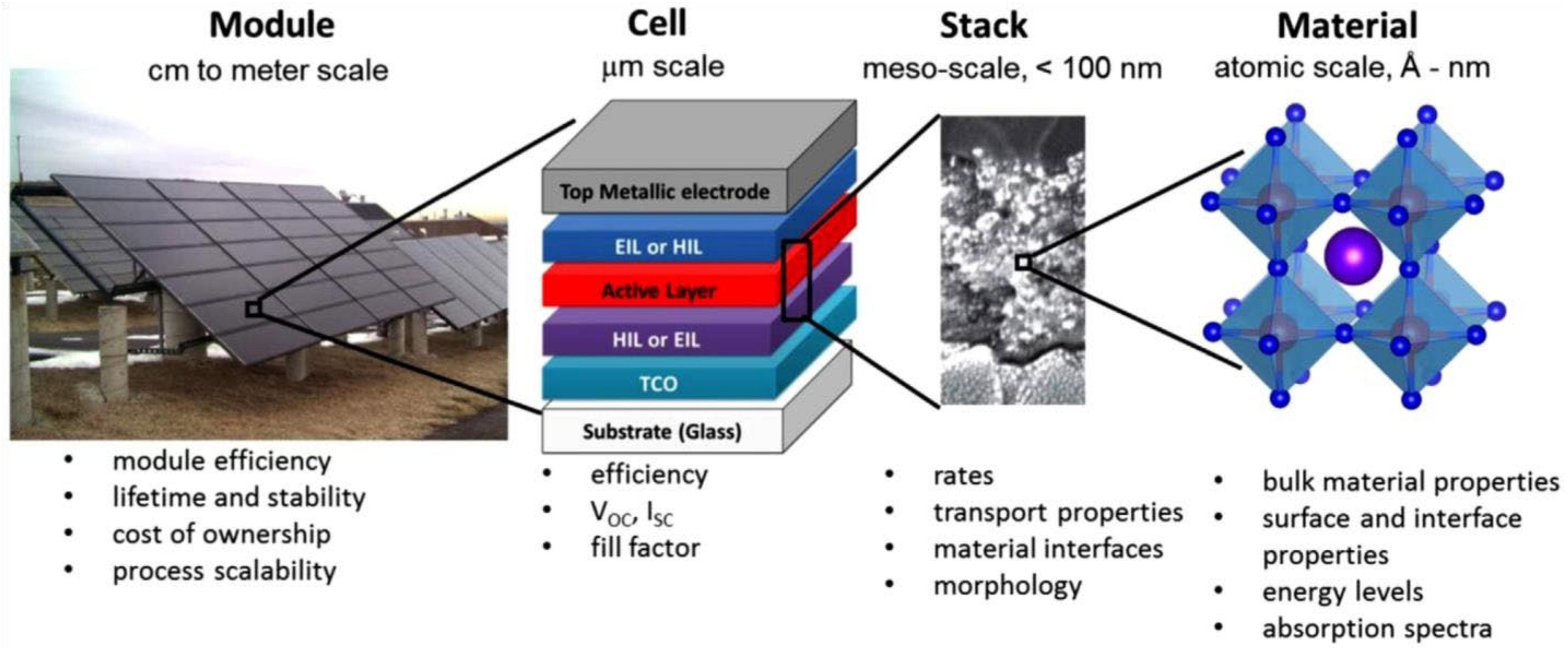
5.1. Multiscale Modelling of PV Technology
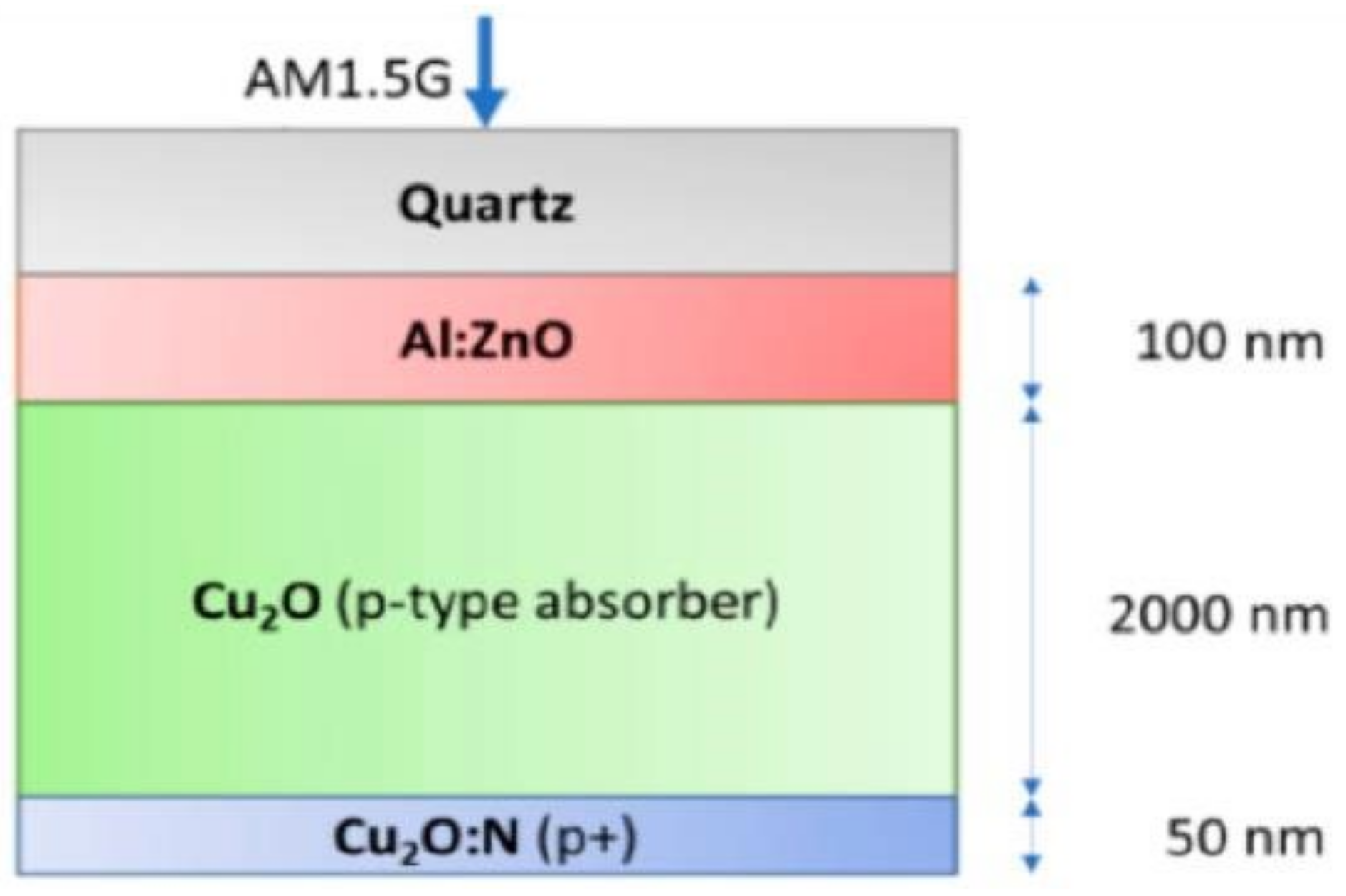
5.2. Diagram of the Cu2O/ZnO Solar Cell Simulation Model
5.3. Simulation Methodology
5.4. Electrical Numerical Modelling for the Two Sub-Cells of the HTSC
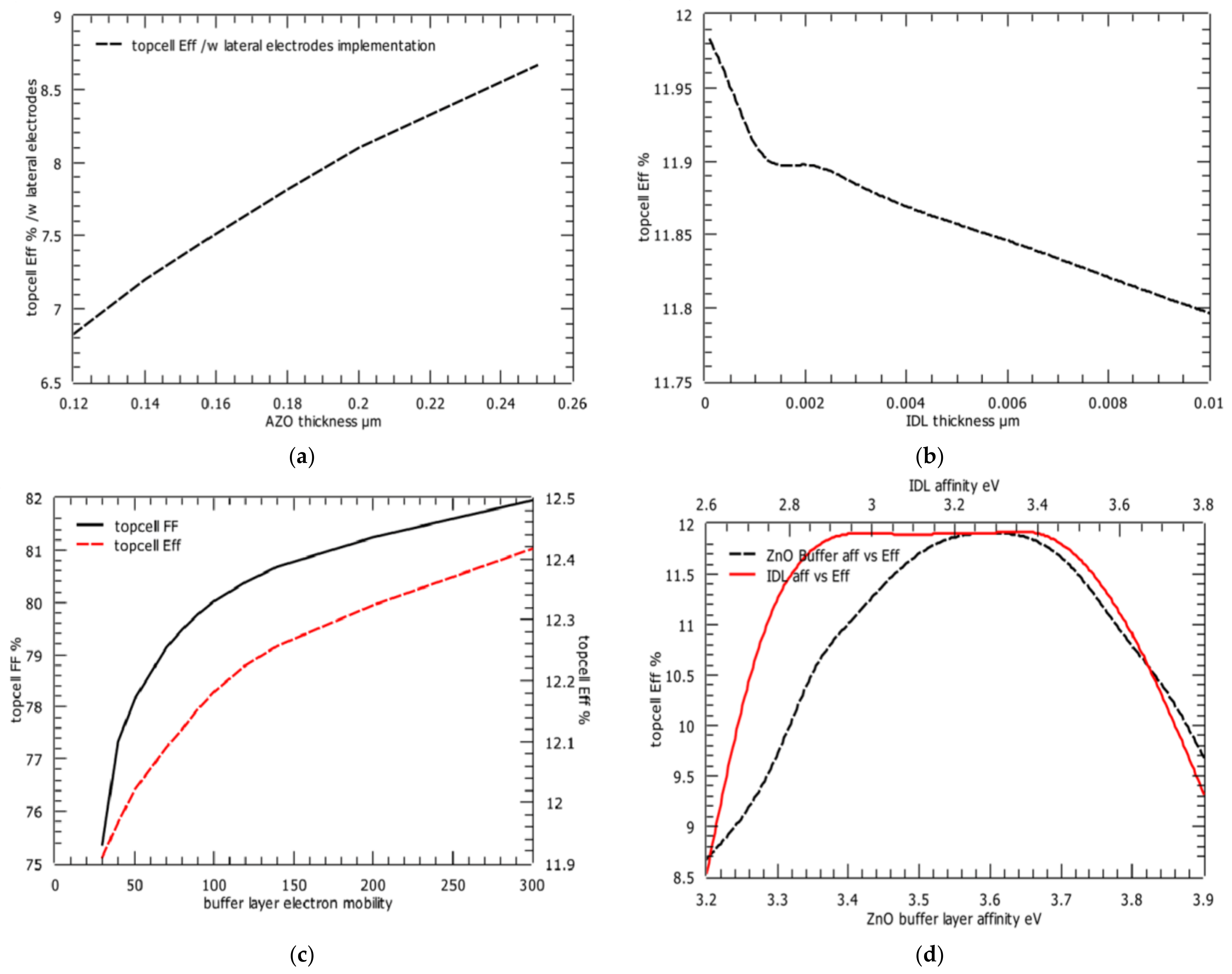
5.4.1. Electrical Modelling of the Top Sub-Cell
- a buffer electron mobility value under 100 cm2/Vs would influence FF and η;
- a comparison of different buffer and IDL materials can be done from the point of view of their affinity. The optimal affinity interval for the buffer layer is 3.4–3.6 eV; it would define the lower conduction band offset with Cu2O absorber layer. The optimal affinity interval for IDL is 2.95–3.4 eV.
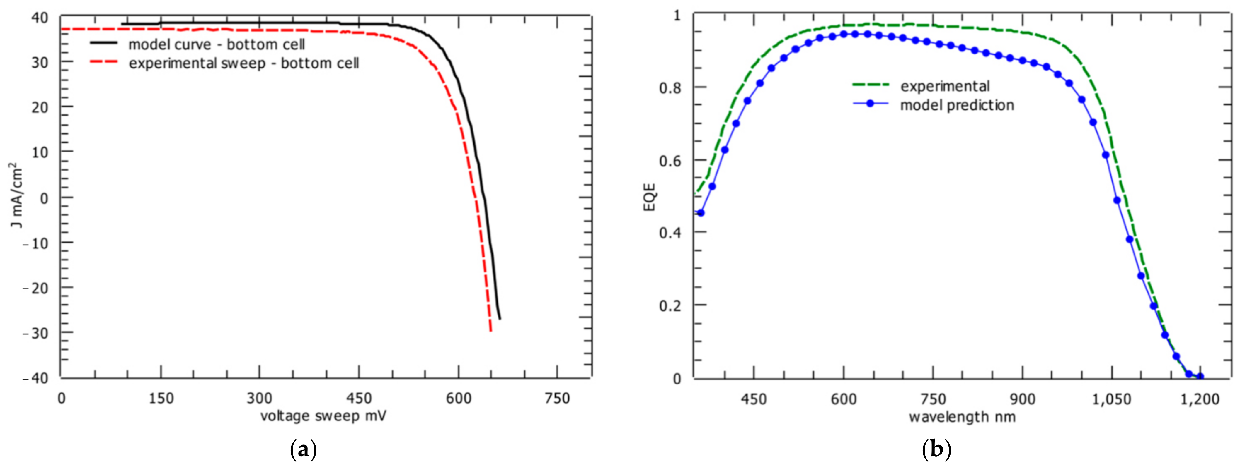
5.4.2. Electrical Modelling of the Bottom Sub-Cell
5.5. Optical Numerical Modelling for the Top Sub-Cell of the HTSC
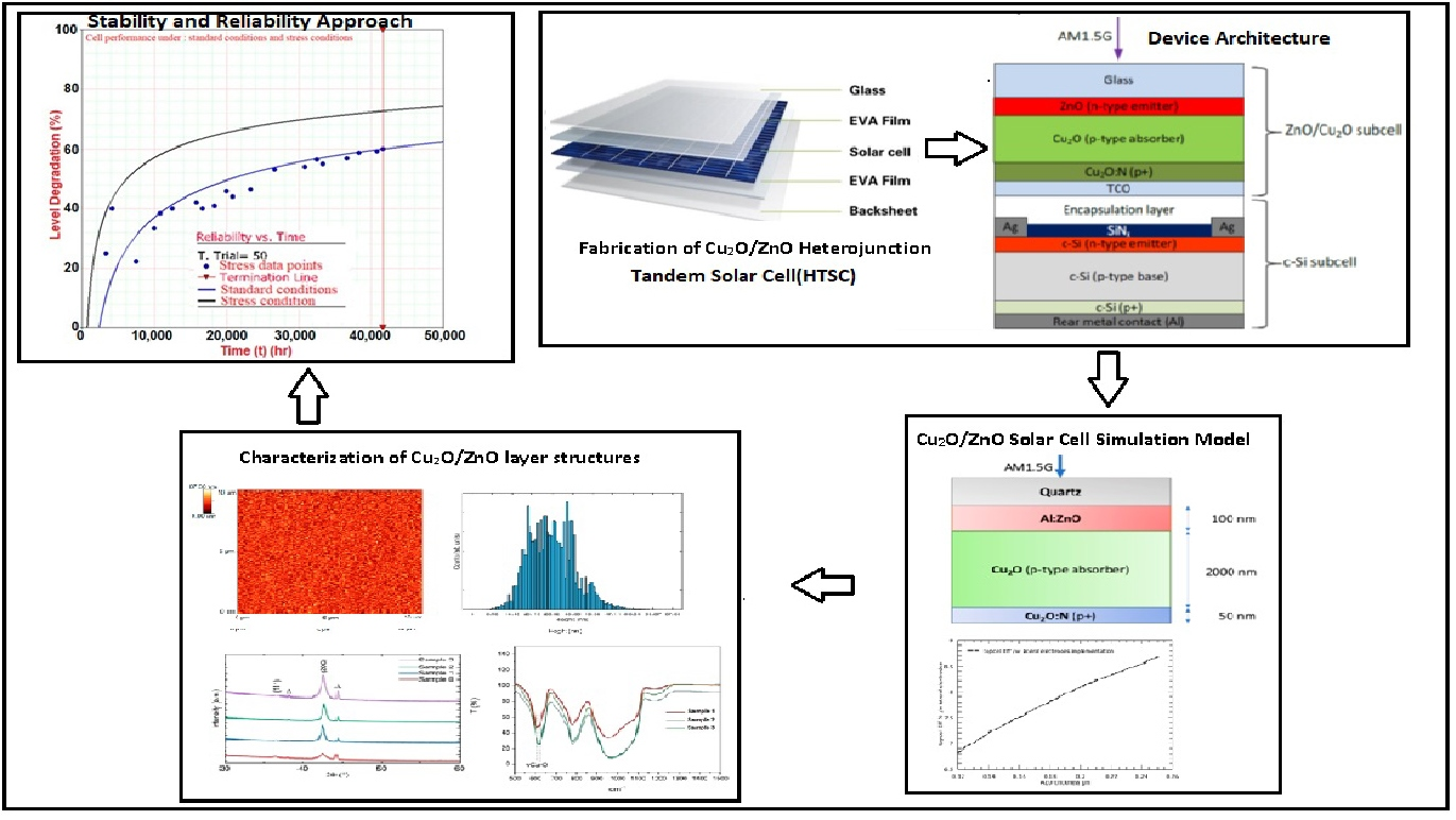
6. Stability and Reliability Approach
6.1. Stability Aspects
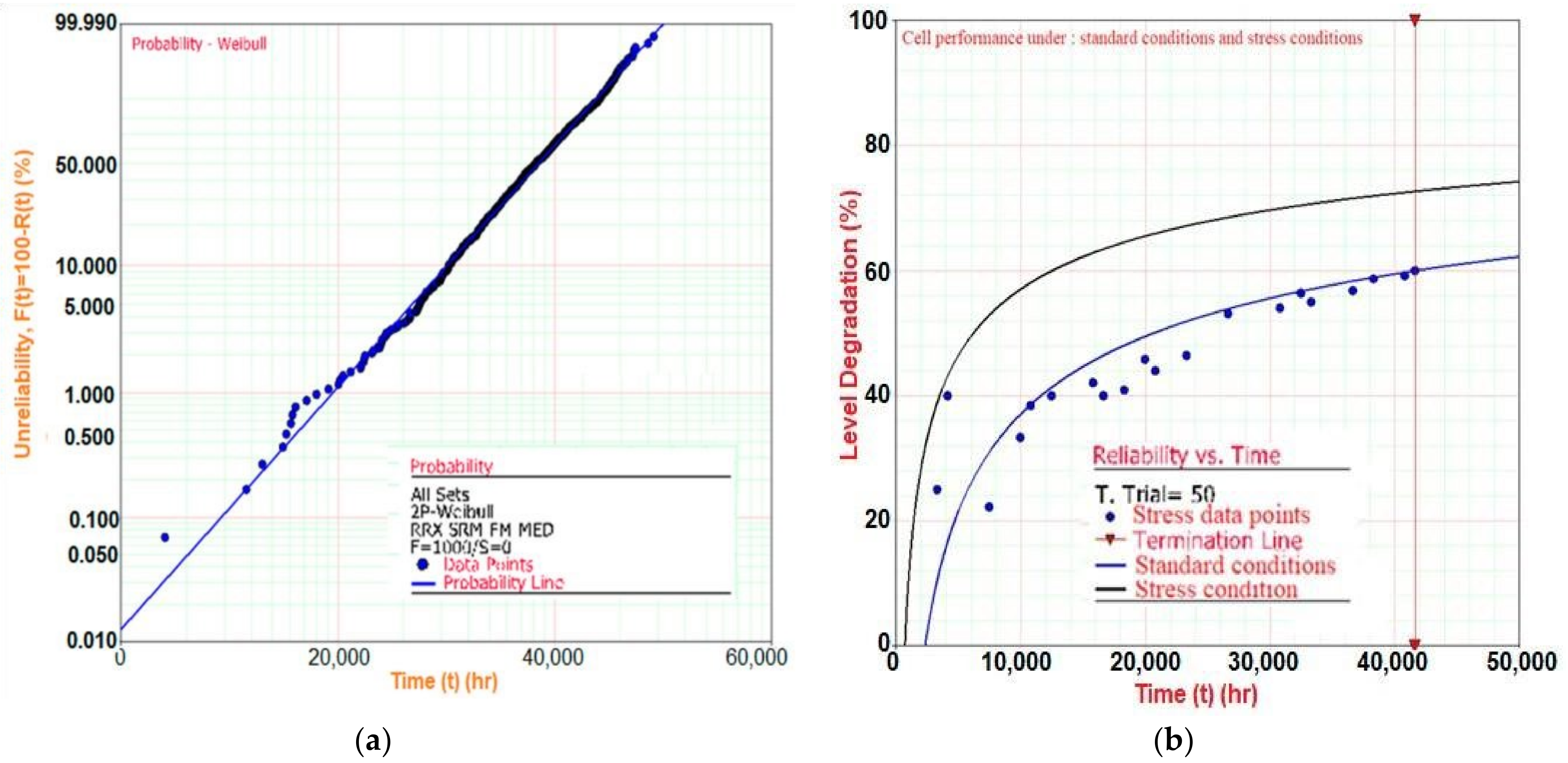
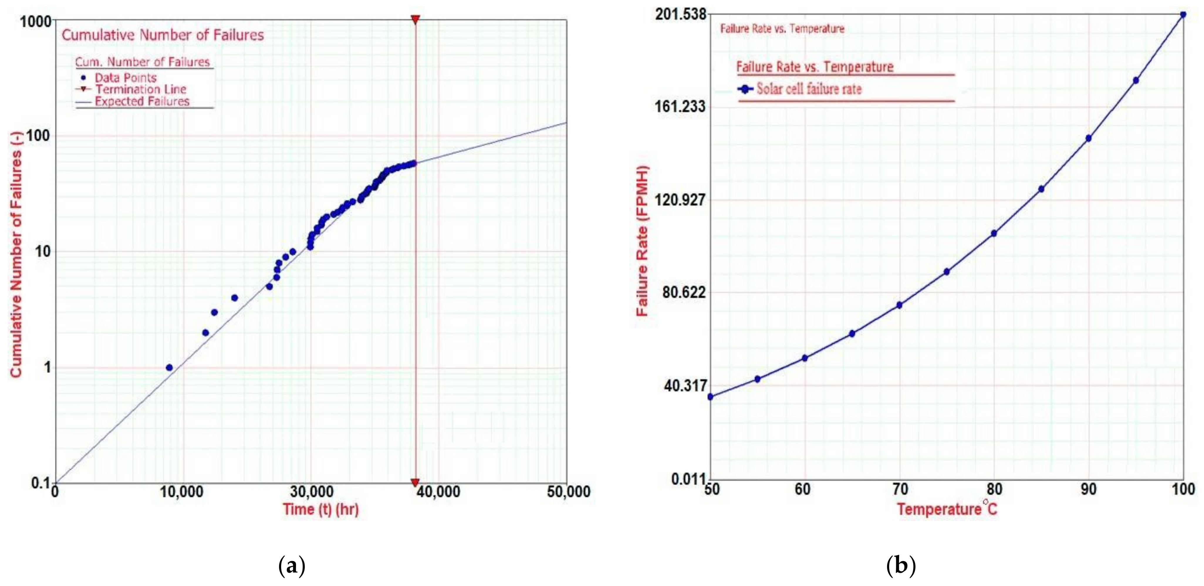
6.2. Methodological Tools for HTSC Reliability
6.3. HTSC Thermal Stability Characteristics
6.4. Reliability of HTSC Based on Si and ZnO
7. Conclusions and Prospects
7.1. Conclusions
- 1.
- 2.
- There were discussed state-of-the-art power conversion efficiencies for HTSC, as well as a comparison analysis with other tandem solar cells such as PSCs.
- 3.
- An unified approach of three main essential issues of HTSC was developed, respectively: (a) experimental evaluation based on fabrication and characterization of these solar devices; (b) their modelling and simulation in order to establish optimized solar cells; (c) thermal stability required for industrial applications of HTSC.
- 4.
- It was analyzed that the HTSC device architecture stressed on four-terminal tandem configuration combines a conventional crystalline silicon sub-cell with a ZnO/Cu2O sub-cell in a stack of independently connected cells.
- 5.
- Cu2O and ZnO layers could be deposited by different methods, namely: (a) magnetron sputtering; (b) electrodeposition; (c) pulsed laser deposition; (d) plasma deposition; (e) photochemical deposition; (f) atomic layer deposition a.o.
- 6.
- Characterization of Cu2O layer structure was defined by: (a) morphological and structural evaluation (SEM, AFM and XRD); (b) optical evaluation (FTIR Spectroscopy, Spectroscopic Ellipsometry). It was remarked that N-doped cuprous oxide heterojunction solar cell could be considered as a bright candidate for high-efficiency solar devices.
- 7.
- Characterization of ZnO layer structure was determined by: (a) structural characterization (SEM, AFM, XRD); (b) optical characterization (UV-VIS Spectroscopy; Photoluminescence Spectroscopy).
- 8.
- Numerical modelling of Cu2O/ZnO HTSC was studied by: (a) electrical modelling and simulation stressing on J-V characteristics and EQE curve; at the same time, the influence of interface defects on the HTSC efficiency could be put in evidence; (b) optical modelling and simulation would be useful for optical losses’ optimization. The performant simulation tools, namely SILVACO and PC1D, could be of great interest for evaluation of optimized parameters.
- 9.
- Stability and reliability approach was discussed. The degradation degree of analyzed solar cells, as well as the solar cell lifetime in normal operation conditions, could be established.
- 10.
- Tandem Solar Cells like PSCs would be considered to be the most promising candidates for integrating with other systems to realize new innovative technologies. The next-generation applications of perovskite-based solar cells include tandem PV cells, space applications, PV-integrated energy storage systems, PV cell-driven catalysis, and BIPVs. The good stability of these devices would be the main challenge to be considered for future applications.
7.2. Prospects
Author Contributions
Funding
Institutional Review Board Statement
Informed Consent Statement
Data Availability Statement
Acknowledgments
Conflicts of Interest
Abbreviations
| ALD | Atomic Layer Deposition |
| AALD | Atmospheric Atomic Layer Deposition |
| AFM | Atomic Force Microscopy |
| AZO | Al-doped ZnO |
| bcc | body-centered cubic |
| Cu2O | Cuprous oxide |
| CVD | Chemical Vapor Deposition |
| d.c. MSP | Direct Current Magnetron Sputtering |
| EC | European Commission |
| ECD | Electro-Chemical Deposition |
| EQE | External quantum efficiency |
| EVA | Ethylene vinyl acetate |
| fcc | face-centered cubic |
| FF | Fill factor |
| FTIR | Fourier transform infrared spectroscopy |
| HASS | High accelerated stress screening |
| HALT | High accelerated life test |
| HTSC | Tandem heterojunction solar cells |
| IBS | Ion Beam Sputtering |
| IDL | Interface defect layer |
| IEA PVPS | International Energy Agency Photovoltaic Power System Programme |
| JRC | Joint Research Centre |
| MSP | Magnetron Sputtering |
| η | Efficiency |
| OPV | Organic photovoltaic |
| PL | Photoluminescence |
| PLD | Pulsed Laser Deposition |
| PV | Photovoltaics |
| r.f. MSP | Radio Frequency Magnetron Sputtering |
| SC | Solar cell |
| SE | Spectroscopic Ellipsometry |
| SEM | Scanning electron microscopy |
| STHSC | Silicon-based tandem heterojunction solar cell |
| UV-VIS | Ultraviolet-visible |
| VAPE | Vacuum Arc Plasma Evaporation |
| XRD | X-ray diffraction |
| ZnO | Zinc Oxide |
References
- Available online: https://ec.europa.eu/energy/en/topics/renewable-energy/renewable-energy-directive (accessed on 1 June 2021).
- European Commission. The Roadmap for Transforming the EU into a Competitive, Low-Carbon Economy by 2050. Available online: https://ec.europa.eu/clima/citizens/eu_en (accessed on 22 June 2015).
- Proposal for a Directive of the European Parliament and the Council. Directive on the Promotion of the Use of Energy from Renewable Sources (Recast), 2016/0382(COD). Available online: http://eur-lex.europa.eu/legal-content/EN/TXT/HTML/?uri=CELEX:52016PC0767R(01)&from=EN (accessed on 30 November 2016).
- Obama, B. The irreversible momentum of clean energy. Science 2017, 355, 126–129. [Google Scholar] [CrossRef] [PubMed] [Green Version]
- Available online: http://www.iea-pvps.org (accessed on 10 April 2018).
- Available online: http://www.ren21.net (accessed on 1 March 2022).
- Available online: https://ec.europa.eu/jrc/en (accessed on 30 May 2022).
- Gambhir, A.; Sandwel, P.; Nelson, J. The future costs of OPV–A bottom-up model of material and manufacturing costs with uncertainty analysis. Sol. Energy Mater. Sol. Cells 2016, 156, 49–58. [Google Scholar] [CrossRef]
- Petrova-Koch, V.; Hezel, R.; Goetzberger, A. High Efficient Low-Cost Photovoltaics: Recent Developments; Springer: Berlin/Heidelberg, Germany, 2008. [Google Scholar]
- Louwen, A.; van Sark, W.G.J.H.M.; Faaij, A.P.C.; Schropp, R.E.I. Re-assessment of net energy production and greenhouse gas emissions avoidance after 40 years of photovoltaics development. Nat. Commun. 2016, 7, 13728. [Google Scholar] [CrossRef] [PubMed] [Green Version]
- Yu, X.; Marks, T.J.; Facchetti, A. Metal oxides for optoelectronic applications. Nat. Mater. 2016, 15, 383–396. [Google Scholar] [CrossRef]
- Zielinska-Raczynska, S.; Ziemkiewicz, D.; Czajkowski, G. Electro-optical properties of Cu2O for P excitons in the regime of Franz-Keldysh oscillations. Phys. Rev. B 2018, 97, 165205. [Google Scholar] [CrossRef] [Green Version]
- Khattak, Y.H.; Baig, F.; Ullah, S.; Marí, B.; Beg, S.; Khan, K. Effect of Cu2O hole transport layer and improved minority carrier life time on the efficiency enhancement of Cu2NiSnS4 based experimental solar cell. J. Renew. Sustain. Energy 2018, 10, 043502. [Google Scholar] [CrossRef]
- Tsur, Y.; Riess, I. Self-compensation in semiconductors. Phys. Rev. B 1999, 60, 8138. [Google Scholar] [CrossRef]
- Dong, C.J.; Yu, W.X.; Xu, M.; Cao, J.J.; Chen, C.; Yu, W.W.; Wang, Y.D. Valence band offset of Cu2O/In2O3 heterojunction determined by X-ray photoelectron spectroscopy. J. Appl. Phys. 2011, 110, 073712. [Google Scholar] [CrossRef]
- Pavan, M.; Rühle, S.; Ginsburg, A.; Keller, D.A.; Barad, H.-N.; Sberna, P.M.; Nunes, D.; Martins, R.; Anderson, A.Y.; Zaban, A.; et al. TiO2/Cu2O all-oxide heterojunction solar cells produced by spray pyrolysis. Sol. Energy Mater. Sol. Cells 2015, 132, 549–556. [Google Scholar] [CrossRef] [Green Version]
- Lahmar, H.; Setifi, F.; Azizi, A.; Schmerber, G.; Dinia, A. On the electrochemical synthesis and characterization of p-Cu2O/n-ZnO heterojunction. J. Alloys Compd. 2017, 718, 36–45. [Google Scholar] [CrossRef]
- Takiguchi, Y.; Miyajima, S. Device simulation of cuprous oxide heterojunction solar cells. Jpn. J. Appl. Phys. 2015, 54, 112303. [Google Scholar] [CrossRef]
- Nordseth, Ø.; Kumar, R.; Bergum, K.; Fara, L.; Dumitru, C.; Craciunescu, D.; Dragan, F.; Chilibon, I.; Monakhov, E.; Foss, S.E.; et al. Metal Oxide Thin-Film Heterojunctions for Photovoltaic Applications. Materials 2018, 11, 2593. [Google Scholar] [CrossRef] [Green Version]
- Nordseth, Ø.; Kumar, R.; Bergum, K.; Fara, L.; Foss, S.E.; Haug, H.; Dragan, F.; Craciunescu, D.; Sterian, P.; Chilibon, I.; et al. Optical analysis of a ZnO/Cu2O subcell in a silicon-based tandem heterojunction solar cell. Green Sustain. Chem. 2017, 7, 57–69. [Google Scholar] [CrossRef] [Green Version]
- Minami, T.; Nishi, Y.; Miyata, T. Efficiency enhancement using a Zn1−xGex-O thin film as an n-type window layer in Cu2O based heterojunction solar cells. Appl. Phys. Express 2016, 9, 052301. [Google Scholar] [CrossRef]
- Gunnæs, A.E.; Gorantla, S.; Løvvik, O.M.; Gan, J.; Carvalho, P.A.; Svensson, B.G.; Monakhov, E.V.; Bergum, K.; Jensen, I.T.; Diplas, S. Epitaxial Strain-Induced Growth of CuO at Cu2O/ZnO Interfaces. J. Phys. Chem. C 2016, 120, 23552–23558. [Google Scholar] [CrossRef]
- White, P.T.; Niraj, L.N.; Kylie, C.R. Tandem Solar Cells Based on High-Efficiency c-Si Bottom Cells: Top Cell Requirements for >30% Efficiency. IEEE J. Photovolt. 2014, 4, 208–214. Available online: https://ieeexplore.ieee.org/document/6626569 (accessed on 9 October 2013). [CrossRef]
- Jacobsen, E.C. Analysis of the ZnO/Cu2O Thin Film Heterojunction for Intermediate Band Solar Cell Applications, see the Chapters 3–6, Respectively: Literature Review, Proposed Design, Methodology and Experimental Setups, Experimental Results and Discussion. Master’s Thesis, NTNU-Norwegian University of Science and Technology, Trondheim, Norway, June 2015; 113p. Available online: https://core.ac.uk/download/pdf/154672771.pdf (accessed on 1 June 2015).
- Tsakalakos, L. (Ed.) Nanotechnology for Photovoltaics; CRC Press: Boca Raton, FL, USA, 2010; Taylor and Francis Group: Abingdon, UK, 2010; 458p. [Google Scholar] [CrossRef]
- De Vos, A. Detailed balance limit of the efficiency of tandem solar cells. J. Phys. D Appl. Phys. 1980, 13, 839. [Google Scholar] [CrossRef]
- National Renewable Energy Laboratory. Research Cell Efficiency Records; National Renewable Energy Laboratory: Washington, DC, USA, 2015.
- Nordseth, Ø.; Fara, L.; Kumar, R.; Foss, S.E.; Dumitru, C.; Muscurel, V.-F.; Drăgan, F.; Crăciunescu, D.; Bergum, K.; Haug, H.; et al. Electro-optical modeling of a ZnO/Cu2O subcell in a silicon-based tandem heterojunction solar cell. In Proceedings of the 33rd European Photovoltaic Solar Energy Conference and Exhibition, Amsterdam, The Netherlands, 25–29 September 2017; pp. 172–177. [Google Scholar]
- Bergum, K.; Riise, H.N.; Gorantla, S.; Lindberg, P.F.; Jensen, I.J.T.; Gunnæs, A.E.; Galeckas, A.; Diplas, S.; Svensson, B.G.; Monakhov, E. Improving carrier transport in Cu2O thin films by rapid thermal annealing. J. Phys. Condens. Matter 2018, 30, 075702. [Google Scholar] [CrossRef]
- Gan, J.; Venkatachalapathy, V.; Svensson, B.G.; Monakhov, E. Influence of target power on properties of CuxO thin films prepared by reactive radio frequency magnetron sputtering. Thin Solid Films 2015, 594, 250–255. [Google Scholar] [CrossRef]
- Ashida, A.; Sato, S.; Yoshimura, T.; Fujimura, N. Control of native acceptor density in epitaxial Cu2O thin films grown by electrochemical deposition. J. Cryst. Growth 2017, 468, 245–248. [Google Scholar] [CrossRef]
- Kwon, J.-D.; Kwon, S.-H.; Jung, T.-H.; Nam, K.-S.; Chung, K.-B.; Kim, D.-H.; Park, J.-S. Controlled growth and properties of p-type cuprous oxide films by plasma enhanced atomic layer deposition at low temperature. Appl. Surf. Sci. 2013, 285, 373–379. [Google Scholar] [CrossRef]
- Avila, J.R.; Peters, A.W.; Li, Z.Y.; Ortuno, M.A.; Martinson, A.B.F.; Cramer, C.J.; Hupp, J.T.; Farha, O.K. Atomic layer deposition of Cu(I) oxide films using Cu(II) bis(dimethylamino-2-propoxide) and water. Dalton Trans. 2017, 46, 5790–5795. [Google Scholar] [CrossRef] [PubMed]
- Izaki, M.; Mizuno, K.-T.; Shinagawa, T.; Inaba, M.; Tasaka, A. Photochemical construction of photovoltaic device composed of p-copper(I) oxide and n-zinc oxide. J. Electrochem. Soc. 2006, 153, C668–C672. [Google Scholar] [CrossRef]
- Jeong, S.; Aydil, E.S. 2010 Structural and electrical properties of Cu2O thin films deposited on ZnO by metal organic chemical vapor deposition. J. Vac. Sci. Technol. A 2010, 28, 1338–1343. [Google Scholar] [CrossRef]
- Siddiqui, H.; Parra, M.R.; Pandey, P.; Singh, N.; Qureshi, M.S.; Haque, Z. A review: Synthesis, characterization and cell performance of Cu2O based material for solar cells. Orient. J. Chem. 2012, 28, 1533–1545. [Google Scholar] [CrossRef]
- Available online: http://www.sputtering-targets.net/blog/advantages-and-disadvantages-of-pulsed-laser-deposition-pld/ (accessed on 8 August 2018).
- Available online: https://julissazhang.wixsite.com/sputtertargets/single-post/2019/12/10/advantages-and-disadvantages-of-magnetron-sputtering (accessed on 1 August 2018).
- Available online: https://www.universitywafer.com/advantages-disadvantages-mocvd.html#:~:text=Metal%20Organic%20Chemical%20Vapor%20Deposition%20Advantages%20and%20Disadvantages,process%20include%20achieving%20a%20uniform%2C%20high-conductivity%20thin%20film (accessed on 1 March 2022).
- Available online: https://www.researchgate.net/publication/332277595_New_Development_of_Atomic_Layer_Deposition_Processes_Methods_and_Applications (accessed on 1 April 2019).
- Ozaveshe Oviroh, P.; Rokhsareh, A.; Pan, D.; Coetzee, R.A.; Jen, T.C. New development of atomic layer deposition: Processes, methods and applications. Sci. Technol. Adv. Mater. 2019, 20, 465–496. [Google Scholar] [CrossRef] [Green Version]
- Fara, L.; Chilibon, I.; Nordseth, Ø.; Craciunescu, D.; Savastru, D.; Vasiliu, C.; Baschir, L.; Fara, S.; Kumar, R.; Monakhov, E.; et al. Complex Investigation of High Efficiency and Reliable Heterojunction Solar Cell Based on an Improved Cu2O Absorber Layer. Energies 2020, 13, 4667. [Google Scholar] [CrossRef]
- Minami, T.; Miyata, T.; Ihara, K.; Minamino, Y.; Tsukada, S. Effect of ZnO film deposition methods on the photovoltaic properties of ZnO–Cu2O heterojunction devices. Thin Solid Films 2006, 494, 47–52. [Google Scholar] [CrossRef]
- Al-Ghamdi, A.A.; Al-Hartomy, O.A.; El Okr, M.; Nawar, A.M.; El-Gazzar, S.; El-Tantawy, F.; Yakuphanoglu, F. Semiconducting properties of Al doped ZnO thin films. Spectrochim. Acta Part A Mol. Biomol. Spectrosc. 2014, 131, 512–517. [Google Scholar] [CrossRef]
- Pal, D.; Singhal, J.; Mathur, A.; Singh, A.; Dutta, S.; Zollner, S.; Chattopadhyay, S. Effect of substrates and thickness on optical properties in atomic layer deposition grown ZnO thin films. Appl. Surf. Sci. 2017, 421, 341–348. [Google Scholar] [CrossRef]
- Habibi, A.; Vatandoust, L.; Aref, S.M.; Naghshara, H. Formation of high performance nanostructured ZnO thin films as a function of annealing temperature: Structural and optical properties. Surf. Interfaces 2020, 21, 100723. [Google Scholar] [CrossRef]
- Ievskaya, Y.; Hoye, R.L.Z.; Sadhanala, A.; Musselman, K.P.; MacManus-Driscoll, J.L. Fabrication of ZnO/Cu2O heterojunctions in atmospheric conditions: Improved interface quality and solar cell performance. Sol. Energy Mater. Sol. Cells 2015, 135, 43–48. [Google Scholar] [CrossRef] [Green Version]
- Minami, T.; Nishi, Y.; Miyata, T. High-efficiency Cu2O-based heterojunction solar cells fabricated using a Ga2O3 thin film as ntype layer. Appl. Phys. Express 2013, 6, 044101. [Google Scholar] [CrossRef] [Green Version]
- Minami, T.; Nishi, Y.; Miyata, T.; Abe, S. Photovoltaic properties in Al doped ZnO/non-doped Zn1-xMgxO/Cu2O heterojunction solar cells. ECS Trans. 2012, 50, 59–68. [Google Scholar] [CrossRef]
- Nishi, Y.; Miyata, T.; Minami, T. The impact of heterojunction formation temperature on obtainable conversion efficiency in n-ZnO/p-Cu2O solar cells. Thin Solid Films 2013, 528, 72–76. [Google Scholar] [CrossRef]
- Lee, Y.S.; Chua, D.; Brandt, R.E.; Siah, S.C.; Li, J.V.; Mailoa, J.P.; Lee, S.W.; Gordon, R.G.; Buonassisi, T. Atomic layer deposited gallium oxide buffer layer enables 1.2 V open-circuit voltage in cuprous oxide solar cells. Adv. Mater. 2014, 26, 4704–4710. [Google Scholar] [CrossRef]
- Minami, T.; Nishi, Y.; Miyata, T.; Nomoto, J. High-Efficiency Oxide Solar Cells with ZnO/Cu2O Heterojunction Fabricated on Thermally Oxidized Cu2O Sheets. Appl. Phys. Express 2011, 4, 062301. [Google Scholar] [CrossRef]
- Lee, S.W.; Lee, Y.S.; Heo, J.; Siah, S.C.; Chua, D.; Brandt, R.E.; Kim, S.B.; Mailoa, J.P.; Buonassisi, T.; Gordon, R.G. Improved Cu2O-based solar cells using atomic layer deposition to control the cu oxidation state at the p–n junction. Adv. Energy Mater. 2014, 4, 1301916. [Google Scholar] [CrossRef]
- Lee, Y.S.; Heo, J.; Siah, S.C.; Mailoa, J.P.; Brandt, R.E.; Kim, S.B.; Gordon, R.G.; Buonassisi, T. Ultrathin amorphous zinc-tinoxide buffer layer for enhancing heterojunction interface. Energy Environ. Sci. 2013, 6, 2112–2118. [Google Scholar] [CrossRef] [Green Version]
- Boughelout, A.; Makaluso, R.; Crupi, I.; Megna, B.; Aida, M.S.; Kecchouane, M. Improved Cu2O/AZO Heterojunction by Inserting a Thin ZnO Interlayer Grown by Pulsed Laser Deposition. J. Electron. Mater. 2019, 48, 4381–4388. [Google Scholar] [CrossRef] [Green Version]
- Mittiga, A.; Salza, E.; Sarto, F.; Tucci, M.; Vasanthi, R. Heterojunction solar cell with 2% efficiency based on a Cu2O substrate. Appl. Phys. Lett. 2006, 88, 163502. [Google Scholar] [CrossRef]
- Salisu, I.K.; Yunusa, A.; Mustafa, M.K.; Ahmad, M.K. and Mohd Khairul, A, Cuprous Oxide (Cu2O) Based Solar Cell Thickness Dependence. Br. J. Phys. Stud. 2022, 1, 1–7. [Google Scholar] [CrossRef]
- Minami, T.; Tanaka, H.; Shimakawa, T.; Sato, H.; Miyata, T. High-efficiency oxide heterojunction solar cells using Cu2O sheets. Jpn. J. Appl. Phys. 2004, 43, L917–L919. [Google Scholar] [CrossRef]
- Hussain, S.; Cao, C.; Nabi, G.; Khan, W.S.; Usman, Z.; Mahmood, T. Effect of electrodeposition and annealing of ZnO on optical and photovoltaic properties of the p-Cu2O/n-ZnO solar cells. Electrochim. Acta 2011, 56, 8342–8346. [Google Scholar] [CrossRef]
- Katayama, J.; Ito, K.; Matsuoka, M.; Tamaki, J. Performance of Cu2O/ZnO solar cell prepared by two-step electrodeposition. J. Appl. Electrochem. 2004, 34, 687–692. [Google Scholar] [CrossRef]
- Fujimoto, K.; Oku, T.; Akiyama, T. Fabrication and characterization of ZnO/Cu2O solar cells prepared by electrodeposition. Appl. Phys. Express 2013, 6, 086503. [Google Scholar] [CrossRef]
- Izaki, M.; Shinagawa, T.; Mizuno, K.-T.; Ida, Y.; Inaba, M.; Tasaka, A. Electrochemically constructed p-Cu2O/n-ZnO heterojunction diode for photovoltaic device. J. Phys. D Appl. Phys. 2007, 40, 3326–3329. [Google Scholar] [CrossRef]
- Marin, A.T.; Muñoz-Rojas, D.; Iza, D.C.; Gershon, T.; Musselman, K.P.; MacManus-Driscoll, J.L. Novel atmospheric growth technique to improve both light absorption and charge collection in ZnO/Cu2O thin film solar cells. Adv. Funct. Matter 2013, 23, 3413–3419. [Google Scholar] [CrossRef]
- Musselman, K.P.; Wisnet, A.; Iza, D.C.; Hesse, H.C.; Scheu, C.; MacManus-Driscoll, J.L.; Schmidt-Mende, L. Strong efficiency improvements in ultra-low-cost inorganic nanowire solar cells. Adv. Mater. 2010, 22, E256–E258. [Google Scholar] [CrossRef]
- Jeong, S.S.; Mittiga, A.; Salza, A.; Masci, A.; Passerini, A. Electrodeposited ZnO/Cu2O heterojunction solar cells. Electrochim. Acta 2008, 53, 2226–2231. [Google Scholar] [CrossRef]
- World Intellectual Property Organization. Solar Cell, Multijunction Solar Cell, Solar Cell Module and Solar Power Generation System, WIPO/PCT, Japan. Patent. WO2019058605A1, 28 March 2019. Available online: https://patentimages.storage.googleapis.com/2e/f5/dc/eb1e0778922963/WO2019058605A1.pdf (accessed on 28 March 2019).
- Wang, Y.; Ghanbaja, J.; Horwat, D.; Yu, L.; Pierson, J.F. Nitrogen chemical state in N-doped Cu2O thin films. Appl. Phys. Lett. 2017, 110, 131902. [Google Scholar] [CrossRef]
- Nordseth, Ø.; Chilibon, I.; Kumar, R.; Bergum, K.; Vasiliu, C.; Iordanescu, R.; Baschir, L.; Savastru, D.; Kiss, A.; Parau, A.; et al. Characterization of Cuprous Oxide Thin Films Prepared by Reactive Direct Current Magnetron Sputtering. Sens. Transducers 2018, 220, 37–44. [Google Scholar]
- Bennett, J.M.; Mattson, L. Introduction to Surface Roughness and Scattering; Optical Society of America: Washington, DC, USA, 1989. [Google Scholar]
- Nordseth, O.; Kumar, R.; Bergum, K.; Chilibon, I.; Fara, L.; Foss, S.E.; Monakhov, E. Nitrogen-doped Cu2O hin films for photovoltaic applications. Materials 2019, 12, 3038. [Google Scholar] [CrossRef] [Green Version]
- JCPDS 78-2076 for Cu2O; International Centre for Diffraction Data-JCPDS: Newtown Square, PA, USA, 1996.
- Nakano, Y.; Saeki, S.; Morikawa, T. Optical bandgap widening of p-type Cu2O films by nitrogen doping. Appl. Phys. Lett. 2009, 94, 022111. [Google Scholar] [CrossRef] [Green Version]
- Reddy, M.H.P.; Pierson, J.F.; Uthanna, S. Structural, surface morphological, and optical properties of nanocrystal line Cu2O and CuO films formed by RF magnetron sputtering: Oxygen partial pressure effect. Phys. Status Solidi A 2012, 209, 1279–1286. [Google Scholar] [CrossRef]
- Sberna, P.M.; Crupi, I.; Moscatelli, F.; Privitera, V.; Simone, F.; Miritello, M. Sputtered cuprous oxide thin films and nitrogen doping by ion implantation. Thin Solid Films 2016, 600, 71–75. [Google Scholar] [CrossRef]
- Ogwu, A.A.; Darma, T.H. A reactive magnetron sputtering route for attaining a controlled core-rim phase partitioning in Cu2O/CuO thin films with resistive switching potential. J. Appl. Phys. 2013, 113, 183522. [Google Scholar] [CrossRef]
- Su, J.; Niu, Q.; Sun, R.; An, X.; Zhang, Y. Investigation of Cu2O films sputtered with ceramic target: Effect of RF power. J. Optoelectron. Adv. Mater. 2018, 20, 441–444. [Google Scholar]
- Gong, J.B.; Dong, W.L.; Dai, R.C.; Wang, Z.P.; Zhang, Z.M.; Ding, Z.J. Thickness dependence of the optical constants of oxidized copper thin films based on ellipsometry and transmittance. Chin. Phys. B 2014, 23, 087802. [Google Scholar] [CrossRef]
- Liau, L.C.-K.; Tang, C.-H. Effect of a Cu2O buffer layer on the efficiency in p-Cu2O/ZnO hetero-junction photovoltaics using electrochemical deposition processing. J. Appl. Electrochem. 2022, 52, 1459–1467. [Google Scholar] [CrossRef]
- Li, J.; Mei, Z.; Liu, L.; Liang, H.; Azarov, A.; Kuznetsov, A.; Liu, Y.; Ji, A.; Meng, Q.; Du, X. Probing defects in nitrogen-doped Cu2O. Sci. Rep. 2014, 4, 7240. [Google Scholar] [CrossRef] [PubMed] [Green Version]
- Hashim, M.S.; Khaleel, R.S. The bioactivities of prepared Ti, Zn, TiO2, ZnO and Al2O3 nanoparticles by rapid breakdown anodization technique. Surf. Interfaces 2020, 20, 100640. [Google Scholar] [CrossRef]
- Powder Diffraction Journal-Volume 1-ICDD. Available online: https://www.icdd.com/powder-diffraction-journal-volume-1/ (accessed on 25 April 2020).
- Full text of “Standard X-ray Diffraction Powder Patterns:-13-Data for 58 Substances”. Available online: https://archive.org/stream/standardxraydiff2513morr/standardxraydiff2513morr_djvu.txt (accessed on 25 April 2020).
- Özdoğan, M.; Yiğen, S.; Çelebi, C.; Utlu, G. The comparison of transient photocurrent spectroscopy measurements of Pulsed Electron Deposited ZnO thin film for air and vacuum ambient conditions. Thin Solid Films 2019, 680, 48–54. [Google Scholar] [CrossRef]
- Zou, T.; Huang, J.; Hu, Y.; Tang, K.; Zhang, Z.; Zhou, X.; Shen, Y.; Zhang, J.; Wang, L.; Lu, Y. CdZnTe thick film radiation detectors with B and Ga co-doped ZnO contacts. Surf. Coat. Technol. 2019, 360, 64–67. [Google Scholar] [CrossRef]
- Singh, G.; Pandey, P.M. Uniform and graded copper open cell ordered foams fabricated by rapid manufacturing: Surface morphology, mechanical properties and energy absorption capacity. Mater. Sci. Eng. A 2019, 761, 138035. [Google Scholar] [CrossRef]
- Urper, O.; Baydogan, N. Effect of Al concentration on optical parameters of ZnO thin film derived by Sol-Gel dip coating technique. Mater. Lett. 2020, 274, 128000. [Google Scholar] [CrossRef]
- Chou, H.S.; Di Yang, K.; Xiao, S.H.; Patil, R.A.; Lai, C.C.; Vincent Yeh, W.C.; Ho, C.H.; Liou, Y.; Ma, Y.R. Temperature dependent ultraviolet photoluminescence in hierarchical Zn, ZnO and ZnO/Zn nanostructures. Nanoscale 2019, 11, 13385–13396. [Google Scholar] [CrossRef]
- Munawar, T.; Iqbal, F.; Yasmeen, S.; Mahmood, K.; Hussain, A. Multi metal oxide NiOCdO-ZnO nanocomposite–synthesis, structural, optical, electrical properties and enhanced sunlight driven photocatalytic activity. Ceram. Int. 2020, 46, 2421–2437. [Google Scholar] [CrossRef]
- Giannouli, M. Current Status of Emerging PV Technologies: A Comparative Study of Dye-Sensitized, Organic, and Perovskite Solar Cells. Int. J. Photoenergy 2021, 2021, 6692858. [Google Scholar] [CrossRef]
- Auf der Maur, M. Multiscale Approaches for the Simulation of Optoelectronics Devices. J. Green Eng. 2016, 5, 133–156. [Google Scholar] [CrossRef]
- Aeberhard, U.; Czaja, P.; Ermes, M.; Pieters, B.E.; Chistiakova, G.; Bittkau, K.; Richter, A.; Ding, K.; Giusepponi, S.; Celino, M. Towards a Multiscale Approach to the Simulation of Silicon Hetero-junction Solar Cells. J. Green Eng. 2016, 5, 11–32. [Google Scholar] [CrossRef] [Green Version]
- Connolly, J.P.; Koduvelikulathu, L.J.; Mencaraglia, D.; Rimada, J.C.; Nejim, A.; Sanchez, G. Multiscale approaches to high efficiency photovoltaics. Renew. Energy Environ. Sustain. 2016, 1, 6. [Google Scholar] [CrossRef]
- Lloyd, M.A.; Siah, S.C.; Brandt, R.E.; Serdy, J.; Johnson, S.W.; Lee, Y.S.; Buinassisi, T. Intrinsic defect engineering of cuprous oxide to enhance electrical transport properties for photovoltaic applications. In Proceedings of the IEEE 40th Photovoltaic Specialists Conference (PVSC), Denver, CO, USA, 8–13 June 2014; pp. 3443–3445. [Google Scholar]
- Tolstova, Y.; Omelchenko, S.T.; Blackwell, R.E.; Shing, A.M. Polycrystalline Cu2O photovoltaic devices incorporating Zn (O, S) window layers. Sol. Energy Mat. Sol. Cells 2017, 160, 340–345. [Google Scholar] [CrossRef] [Green Version]
- Robertson, J.; Falabretti, B. Band o sets of high K gate oxides on III-V semiconductors. J. Appl. Phys. 2006, 100, 014111. [Google Scholar] [CrossRef]
- Brandt, R.E.; Young, M.; Hejin, H.P.; Dameron, A.; Chua, D.; Lee, S.Y.; Teeter, G.; Gordon, R.; Buonassisi, T. Band o_sets of ntype electron-selective contacts on cuprous oxide (Cu2O) for photovoltaics. Appl. Phys. Lett. 2014, 105, 263901. [Google Scholar] [CrossRef]
- PV Lighthouse. Available online: https://www.pvlighthouse.com.au/ (accessed on 20 January 2020).
- Baker-Finch, S.C.; McIntosh, K.R. OPAL 2: Rapid optical simulation of silicon solar cells. In Proceedings of the 38th IEEE Photovoltaic Specialists Conference, Austin, TX, USA, 3–8 June 2012; pp. 265–271. [Google Scholar]
- Dumitru, C.; Muscurel, V.; Nordseth, O.; Fara, L.; Sterian, P. Optimization of electro-optical performance and material parameters for a tandem metal oxide solar cell. In Proceedings of the International Conference on Computational Science and Its Applications–ICCSA, Melbourne, Australia, 2–5 July 2018; pp. 573–582. [Google Scholar]
- Murali, D.S.; Kumar, S.; Choudhary, R.J.; Wadikar, A.D.; Jain, M.K.; Subrahmanyam, A. Synthesis of Cu2O from CuO thin films: Optical and electrical properties. AIP Adv. 2015, 5, 047143. [Google Scholar] [CrossRef]
- Todorov, T.K.; Reuter, K.B.; Mitzi, D.B. High-efficiency solar cell with earth-abundant liquid-processed absorber. Adv. Mater. 2010, 22, E156–E159. [Google Scholar] [CrossRef]
- Hodes, G.; Cahen, D. Photovoltaics: Perovskite cells roll forward. Nat. Photonics 2014, 8, 87–88. [Google Scholar] [CrossRef]
- Hailegnaw, B.; Kirmayer, S.; Edri, E.; Hodes, G.; Cahen, D. Rain on methylammonium lead iodide based perovskites: Possible environmental effects of perovskite solar cells. J. Phys. Chem. Lett. 2015, 6, 153–157. [Google Scholar] [CrossRef]
- Reliability Engineering Software Products–ReliaSoft. Available online: https://www.reliasoft.com.reliasoft.com (accessed on 20 January 2019).
- Sharma, V.; Chandel, S.S. Performance and degradation analysis for long term reliability of solar photovoltaic systems: A review. Renew. Sustain. Energy Rev. 2013, 27, 753–767. [Google Scholar] [CrossRef]
- Guo, D.; Brinkman, D.; Shaik, A.R.; Ringhofer, C.; Vasileska, D. Metastability and reliability of CdTe solar cells. J. Phys. D Appl. Phys. 2018, 51, 153002. [Google Scholar] [CrossRef]
- Fara, L.; Craciunescu, D. Reliability analysis of photovoltaic systems for specific applications. In Reliability and Ecological Aspects of Photovoltaic Modules; Gok, A., Ed.; Intech Open: London, UK, 2020; pp. 79–92. [Google Scholar]
- Ye, F.; Zeng, J.J.; Qiu, Y.B.; Cai, X.M.; Wang, B.; Wang, H.; Zhang, D.P.; Fan, P.; Roy, V.A.L. Deposition-rate controlled nitrogen-doping into cuprous oxide and its thermal stability. Thin Solid Films 2019, 674, 44–51. [Google Scholar] [CrossRef]
- Wibowo, A.; Marsudi, M.A.; Amal, M.I.; Ananda, M.B.; Stephanie, R.; Ardy, H.; Diguna, L.J. ZnO nanostructured materials for emerging solar cell applications. RSC Adv. 2020, 10, 42838–42859. [Google Scholar] [CrossRef]
- Abdu, Y.; Musa, A.O. Copper (I) oxide (Cu2O) based solar cells-A review. Bayero J. Pure Appl. Sci. 2009, 2, 8–12. [Google Scholar]
- Chevallier, C.; Bose, S.; Hamady, S.O.S.; Fressengeas, N. Numerical investigations of the impact of buffer germanium composition and low cost fabrication of Cu2O on AZO/ZnGeO/Cu2O solar cell performances. EPJ Photovolt. 2021, 12, 3. [Google Scholar] [CrossRef]
- Soonmin, H. A Review of Metal Oxide Thin Films in Solar Cell Applications. Int. J. Thin Film Sci. Technol. 2022, 11, 37–45. [Google Scholar] [CrossRef]
- Liu, Y.; Li, Y.; Wu, Y.; Yang, G.; Mazzarella, L.; Procel-Moya, P.; Tamboli, A.C.; Weber, K.; Boccard, M.; Isabella, O.; et al. High-Efficiency Silicon Heterojunction Solar Cells: Materials, Devices and Applications. Mater. Sci. Eng. R 2020, 142, 100579. [Google Scholar] [CrossRef]
- Ehsan, R.; Zubair, A. Review on two-terminal and four-terminal crystalline-silicon/perovskite tandem solar cells; progress, challenges, and future perspectives. Energy Rep. 2022, 8, 5820–5851. [Google Scholar] [CrossRef]
- Park, J.H.; Ji, S.G.; Park, I.J.; Hwang, S.K.; Lim, H.W.; Kim, J.Y. Sub-cell characterization of two-terminal perovskite/silicon tandem solar cells. Cell Rep. Phys. Sci. 2022, 3, 101076. [Google Scholar] [CrossRef]
- Chander, S.; Kant Tripathi, S. Recent advancement in efficient metal oxide-based flexible perovskite solar cells: A short review. Mater. Adv. 2022, 3, 7198–7211. [Google Scholar] [CrossRef]
- McMahon, W.E.; Geisz, J.F.; Buencuerpo, J.; Warren, E.L. A framework for comparing the energy production of photo voltaic modules using 2-, 3-, and 4-terminal tandem cells. Sustain. Energy Fuels 2023, 7, 461–470. [Google Scholar] [CrossRef]
- Available online: https://www.researchgate.net/publication/359389404_Analysis_of_Silicon-perovskite_Tandem_Solar_Cells_with_Transition_Metal_Oxides_as_Carrier_Selective_Contact_Layers (accessed on 1 March 2022).


| Type of Junction | PCE % | Voc | Deposition Method | Ref. |
|---|---|---|---|---|
| Cu2O-based junctions developed in vacuum | ||||
| AZO/Ga2O3/Cu2O | 5.38 | 0.8 | PLD on Cu2O sheet | [48] |
| AZO/Zn0.91Mg0.09O/Cu2O | 4.3 | 0.8 | PLD on Cu2O sheet | [49] |
| AZO/ZnO/Cu2O | 4.12 | 0.72 | PLD on Cu2O sheet | [50] |
| AZO/Ga2O3/Cu2O | 3.97 | 1.2 | ALD | [51] |
| AZO/ZnO/Cu2O | 3.83 | 0.69 | PLD on Cu2O sheet | [52] |
| AZO/a-ZTO/Cu2O | 2.85 | 0.62 | ALD | [53] |
| AZO/a-ZTO/Cu2O | 2.65 | 0.55 | ALD | [54] |
| AZO/Cu2O | 2.53 | 0.55 | PLD on Cu2O sheet | [55] |
| ITO/ZnO/Cu2O | 2.01 | 0.6 | IBS | [56] |
| ZnO:Ga/Cu2O | 1.52 | 0.41 | VAPE | [57] |
| AZO/Cu2O | 1.39 | 0.4 | dc-MSP | [57] |
| AZO/Cu2O | 1.21 | 0.41 | PLD | [58] |
| AZO/Cu2O | 0.24 | 0.34 | electrodeposition | [59] |
| Cu2O-based junctions developed without vacuum | ||||
| ZnO/Cu2O | 0.12 | 0.19 | ECD | [60] |
| ZnO/Cu2O | 1.43 | 0.54 | ECD | [61] |
| ZnO/Cu2O | 1.28 | 0.59 | ECD | [62] |
| ZnO/Cu2O/Cu2O+ | 0.9 | 0.32 | ECD | [63] |
| ZnO/Cu2O | 0.47 | 0.28 | ECD | [64] |
| ZnO/Cu2O | 0.41 | 0.32 | ECD | [65] |
| ZnO/Cu2O | 1.46 | 0.49 | AALD | [47] |
| ITO/Zn0.79Mg0.21O/Cu2O | 2.2 | 0.65 | AALD | [47] |
| Sample Name | Gas Flow Conditions | Grains Size (nm) |
|---|---|---|
| Sample 0 | Ar/O2 was fixed at 42.5/7.5 sccm undoped | 20–90 |
| Sample 1 | (Ar/O2 was fixed at 42.5/7.5 sccm) N-doped 3 sccm | 20–48 |
| Sample 2 | (Ar/O2 was fixed at 42.5/7.5 sccm) N-doped 1 sccm | 30–54 |
| Sample 3 | (Ar was varied at 41.5 sccm, O2 was fixed at 7.5 sccm) | 40–88 |
| Sample Deposited on Quartz | RRMS (nm) | Height Distribution Standard Deviation (nm) |
|---|---|---|
| Sample 0 | 6.3 | 7.8 |
| Sample 1 | 4.7 | 5.8 |
| Sample 2 | 4.2 | 4.5 |
| Sample 3 | 3.9 | 4.2 |
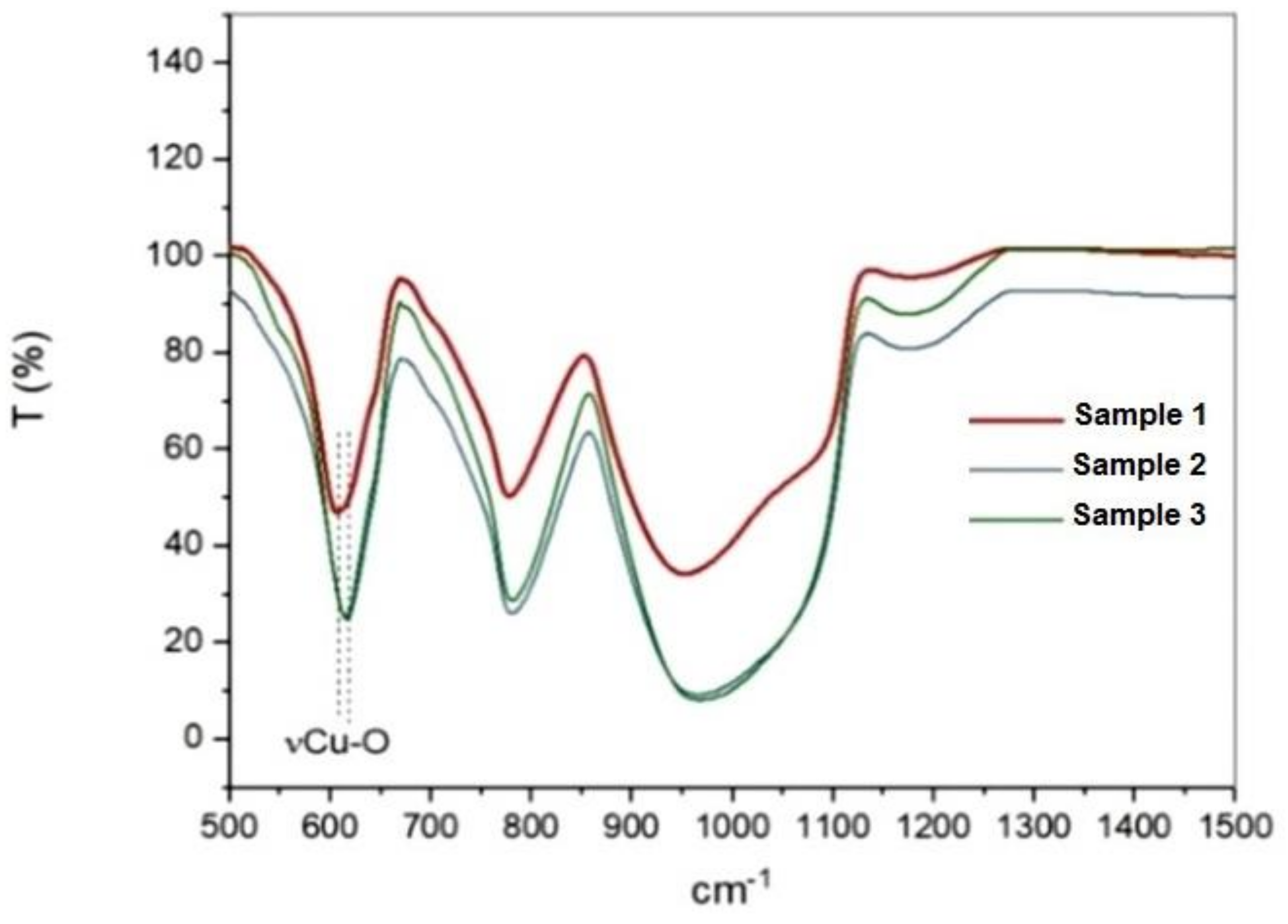
| Sample Name | ν Cu2O (cm−1) |
|---|---|
| Sample 1 | 608 |
| Sample 2 | 616 |
| Sample 3 | 615 |
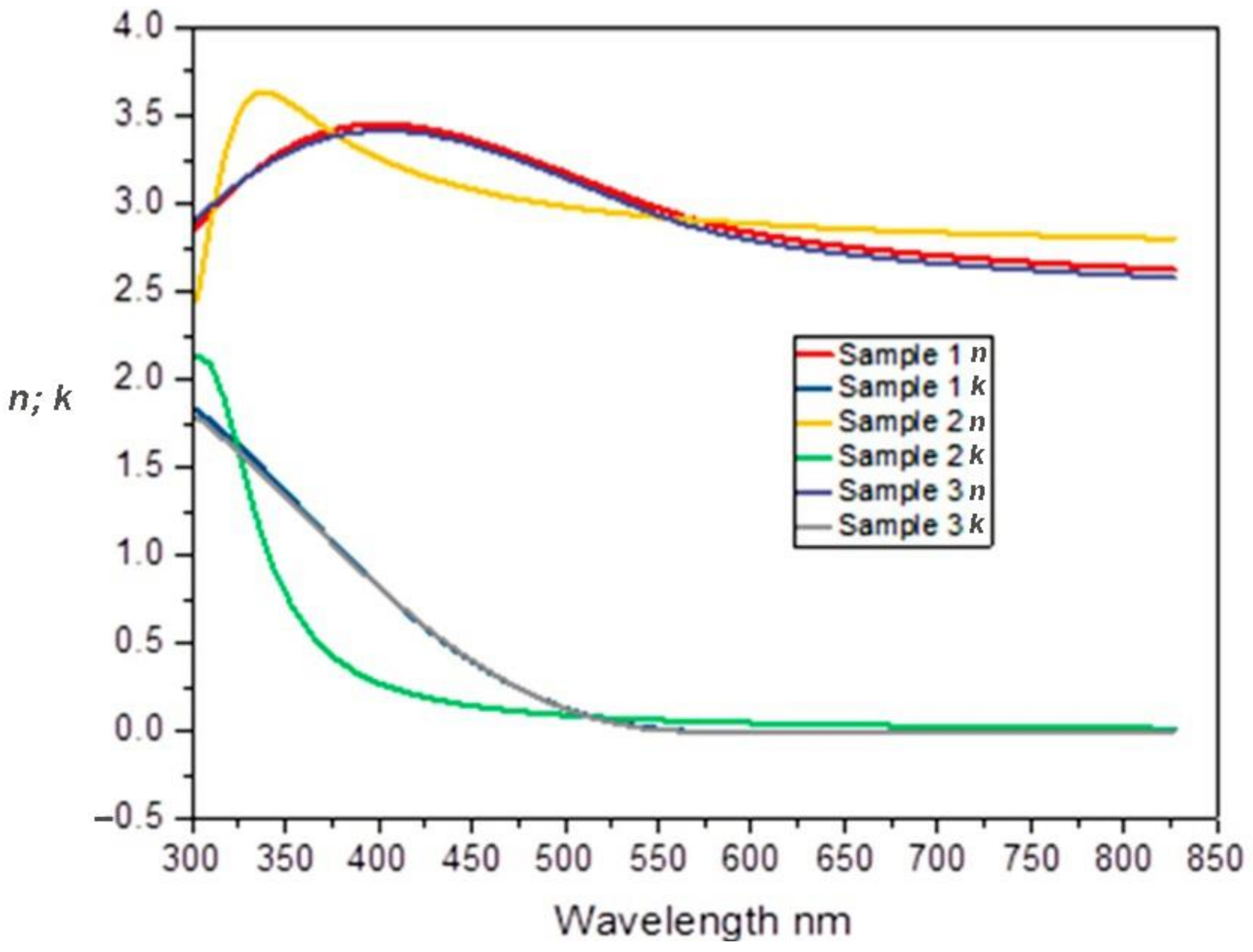
| Sample Name | Sample 1 | Sample 2 | Sample 3 |
|---|---|---|---|
| Band gap (eV): | 2.17 | 2.14 | 2.17 |
| Surface roughness (nm): | 15.9 | 19.6 | 17.2 |
| Efficiency (%) | Active Layer/Absorber | Carrier Transporting Material | Innovative Materials/Techniques | Institution/Company | |
|---|---|---|---|---|---|
| DSSC | 13.0 | TiO2 dye-sensitized semiconductor | Cobalt redox couple electrolyte | Panchromatic porphyrin sensitizers | EPFL |
| PSC | 25.2 | FAPbI 3-based perovskite | Spiro-MeOTAD | Minimizing the deformation of photoactive layers by changing the type and ratio of ions | UNIST |
| Tandem PSC/Si | 29.5 | Monolithic perov-skite PbI2-based top cell/Si bottom cell | Methyl-substituted carbazole monolayer/C60 | Self-assembled carbazole-based monolayer with methyl group substitution | Oxford PV |
| Tandem PSC/CIGS | 24.2 | Monolithic two-terminal triple-cation PSC/CIGS | Poly [bis(4-phenyl) (2,4,6-trimethylphenyl) amine] (PTAA)/C60 | Rubidium-based self-assembled monolayer | HZB |
| OPV | 18.2 | PBDB-T-2F:BTP-eC9 | PEDOT:PSS | Chlorinated nonfullerene acceptor | SJTU/BUAA |
| Parameter Name | Parameter Value |
|---|---|
| Open circuit voltage, VOC (mV) | 625.16 |
| Fill Factor, FF (%) | 76.83 |
| Series resistance, RS (ohm/cm2): | 0.196 |
| Shunt resistance, RSH (ohm/cm2): | 2382.8 |
Disclaimer/Publisher’s Note: The statements, opinions and data contained in all publications are solely those of the individual author(s) and contributor(s) and not of MDPI and/or the editor(s). MDPI and/or the editor(s) disclaim responsibility for any injury to people or property resulting from any ideas, methods, instructions or products referred to in the content. |
© 2023 by the authors. Licensee MDPI, Basel, Switzerland. This article is an open access article distributed under the terms and conditions of the Creative Commons Attribution (CC BY) license (https://creativecommons.org/licenses/by/4.0/).
Share and Cite
Fara, L.; Chilibon, I.; Craciunescu, D.; Diaconu, A.; Fara, S. Review: Heterojunction Tandem Solar Cells on Si-Based Metal Oxides. Energies 2023, 16, 3033. https://doi.org/10.3390/en16073033
Fara L, Chilibon I, Craciunescu D, Diaconu A, Fara S. Review: Heterojunction Tandem Solar Cells on Si-Based Metal Oxides. Energies. 2023; 16(7):3033. https://doi.org/10.3390/en16073033
Chicago/Turabian StyleFara, Laurentiu, Irinela Chilibon, Dan Craciunescu, Alexandru Diaconu, and Silvian Fara. 2023. "Review: Heterojunction Tandem Solar Cells on Si-Based Metal Oxides" Energies 16, no. 7: 3033. https://doi.org/10.3390/en16073033