1. Introduction
The Tesla coil and Tesla Tower’s introduction in the early 20th century triggered the research on wireless power transfer (WPT) [
1]. Nicola Tesla was able to light a light bulb held barehanded within a certain distance of the Tesla Tower. In the last decade, the demand for electronic handheld and compact devices (mobile phones, laptops, tablets, etc.) has increased, which led Massachusetts Institute of Technology (MIT) researchers in 2007 to introduce a wireless power transfer method called strong magnetic coupling resonances [
2]. The researchers of this paper were able to deliver power to a 60 W light bulb at a distance of 2 m. The research and development of WPT technology are currently ongoing, and are nearing a standardization and commercialization phase. Currently, WPT technology can supply charges to electronic handheld devices, autonomous devices, and electric vehicles.
WPT technology utilizes electromagnetic fields to transmit power to the receiver, which can be accomplished through various methods, including inductive WPT, capacitive WPT [
3], radio frequency [
4], and laser [
5]. Inductive and capacitive WPTs are particularly effective for delivering power over short distances [
6]. Currently, researchers studying WPT are developing a system with better distance, better power, and better efficiency [
7,
8,
9,
10]. At present, WPT research is focused on exploring the system architecture and optimization design [
11]. The most basic circuit for making a WPT system uses a voltage source and coils in the primary and secondary circuit [
12]. The current through the coils enables a magnetic field around the coils and creates self-inductance and mutual inductance between the coils [
13]. However, this minimum WPT circuit delivers a smaller amount of power compared to a direct connection. Therefore, to increase the amount of power absorbed by the load, an additional inductor or capacitor is needed in the primary or secondary circuit, or in both. This method is known as the compensation technique [
14,
15].
The coil design is an essential factor in the WPT circuit [
16,
17], since it influences the parasitic resistances. High parasitic resistance can decrease the transmitted power, while low parasitic resistance leads to increased power and high efficiency [
18]. Thus, researchers want to reduce or even eliminate the effect of the coils’ parasitic resistance on the primary and secondary side by designing a WPT system that works at the resonant frequency. Hence, the L (coil) and C (capacitor) pair component is mainly used on the primary side and secondary side to form the series–series (SS), series–parallel (SP), parallel–series (PS), and parallel–parallel (PP) WPT circuits [
19]. Researchers have explored the optimal operating points to find the best transfer efficiency or best power by analyzing and avoiding the frequency splitting issues. Frequency splitting is a WPT phenomenon where the peak divides if the coupling coils are greater than the critical coupling [
20]. Therefore, if frequency splitting occurs, the inductance, capacitance, or distance needs to be optimized for better power delivery [
21]. Current research on WPT optimization has been reviewed in [
22]. The optimization approach has been applied in various methods, such as impedance matching [
23,
24,
25], parameter optimization [
26,
27], and the use of artificial intelligence [
28,
29].
Since research on series WPT circuits usually focuses on the dual-capacitor circuit, the single-capacitor circuit is under evaluated and under reviewed. This circuit can be considered a simple compensation circuit, since there is no capacitor on the secondary side. Finding the resonant frequency operations in this circuit is challenging, since it only has a primary-side capacitor. Therefore, the question regarding what will happen if we omit the capacitor on the secondary side needs to be answered.
This study proposes carrying out an optimization approach in a primary-side single-capacitor WPT circuit to obtain high-power WPT. This study focuses on the formal methods by compensating for the circuit with the optimum point of the capacitor and frequency. The maximum power objective function is calculated from the steady-state analysis process. Furthermore, a formula determining the optimum points from the capacitor and frequency values is presented. By choosing the capacitor and the frequency value as the optimum points, we also prove that the optimal condition can be maintained, even when there is a change in the system coupling coefficient or load.
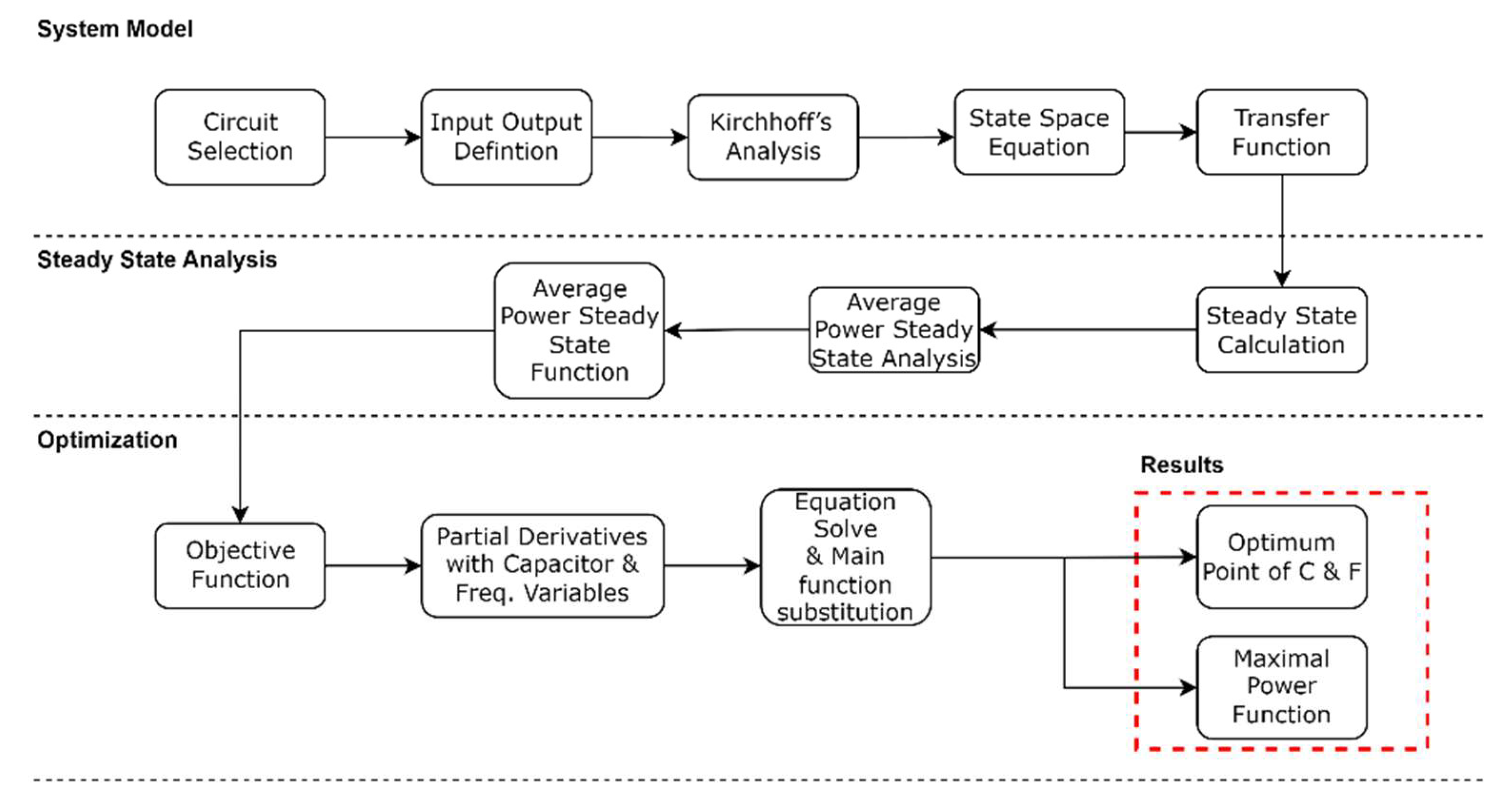
2. Methods
The proposed approach (
Figure 1) consists of three phases: a system model, a steady-state analysis, and an optimization phase. The system model formulizes the transfer function from the primary-side single-capacitor circuit. The state-space variables are obtained corresponding to the input and output definition using Kirchhoff’s circuit law. Next, the state-space matrix is formed and calculated using the state-space equation to obtain the system transfer function [
30]. The second phase consists of analyzing the system’s steady-state conditions. In this phase, a steady-state function is obtained by considering the input signal and the system transfer function. The last phase is the optimization phase, which maximizes the objective function obtained from the steady-state equation. A partial derivative from the objective function, with respect to the capacitor and frequency, was obtained. The solutions from the simultaneous partial derivative equation produce an optimum point capacitor and a frequency equation. The function of the maximal power is obtained by substituting both optimum point equations with an objective function.
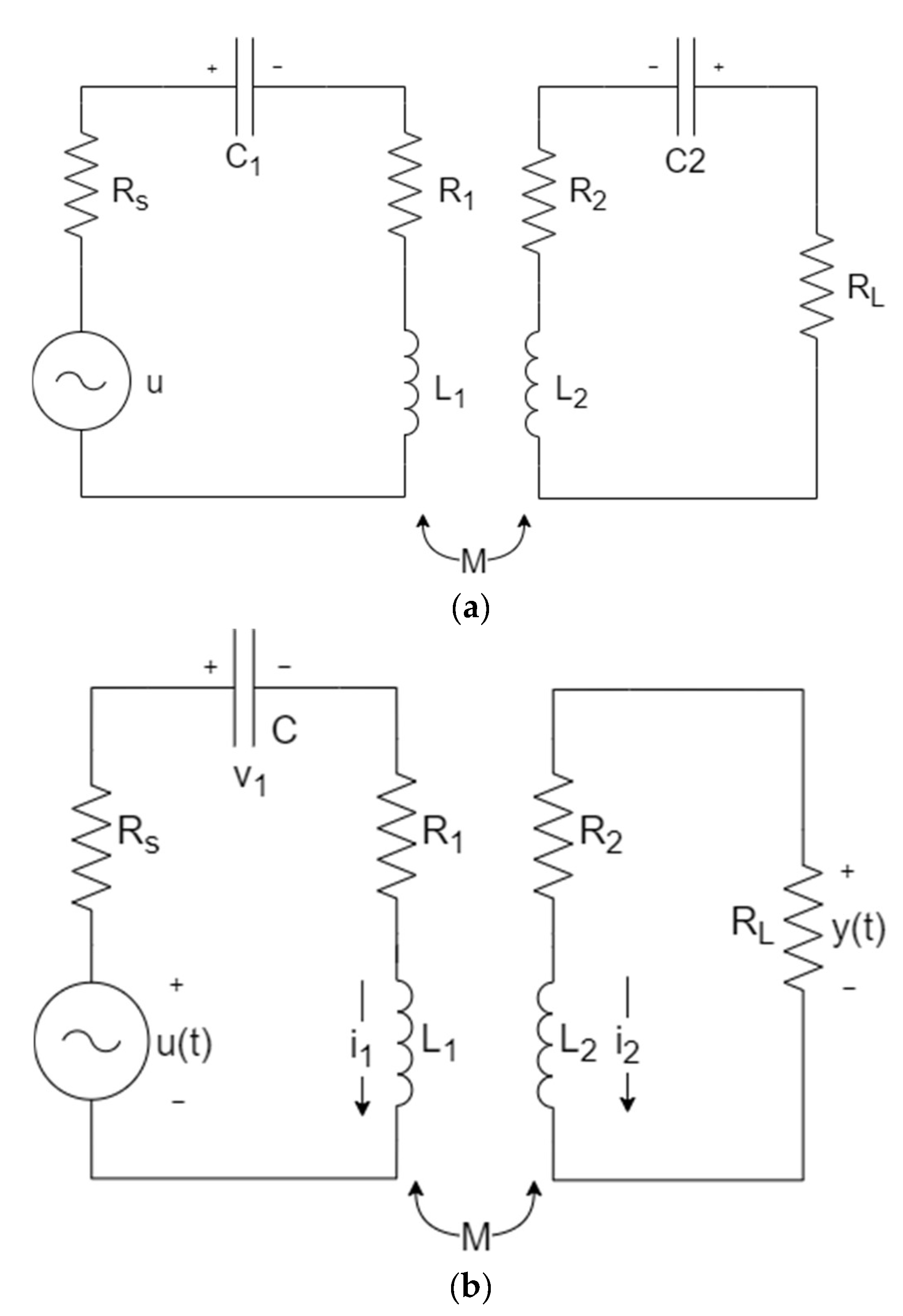
2.1. Circuit Topologies of Wireless Power Transfer
Figure 2a is a schematic of the most popular series type of WPT circuit, where the WPT circuit transfer power originates at the power source on the primary side to load
on the secondary side. A couple of inductors (
and
) are necessary to realize wireless power transfer using an electromagnetic field. The circuit is compensated with capacitors on both sides to apply the idea of resonance, as is shown in
Figure 2a.
Figure 2b shows a schematic of the series connection type of the WPT system, where the capacitor
on the secondary side is omitted. We cannot simply use the idea of resonance because of the lack of symmetry. Instead, we will optimize circuit component parameters to obtain the maximal power at the load
independent of resonance. The primary circuit consists of an input voltage source (
u) with an internal resistance
), a capacitor (
C), the transmitter inductor (
), and the internal resistance (
). The secondary circuit consists of the receiver inductor (
with its internal resistance (
) and the load (
Let
M and
K be the mutual inductance and coupling coefficients between the transmitter and receiver inductors, which can be replaced by Equation (1).
2.2. Circuit Equation
We will analyze the wireless power transfer circuit in
Figure 2b. Let us start with the circuit equation in the form of Equation (2).
where
are state-space variables,
u is the input, and
y is the output. Equivalently, we define our state-space representations as Equation (3).
where
The transfer of Function (2) from
u to
y is given by
2.3. Steady-State Function
Our circuit equation stimulated by a periodic input has a periodic solution where the period is the same as the input since the differential equation is a linear time-invariant system. If the system is stable, i.e., all the eigenvalues of matrix
A have a negative real part, then the periodic solution will be asymptotically stable. In other words, any solution starting with any initial value will behave as the periodic solution when enough time has passed; thus, the periodic solution is often called a steady-state solution [
31]. In the beginning, it is important to obtain the steady-state function to obtain the exact calculation under the steady-state conditions [
32,
33]. In this computation, we use the symbolic computation [
34] of the
y(
t) output, described as
. A similar approach was also conducted by [
35] to perform the time domain analysis and modeling before the optimization process. Since this study analyzes the circuit’s behavior using the sine wave input, the input function
u(t) can be described as Equation (7), where
is the amplitude of the input voltage.
From the sinusoidal input of Equation (7), the steady-state function of
can be described by Equation (8) [
36].
is the power at the load
in the steady state. The average of
over a period is called the average power at the load
. From Equations (8) and (9), the average power can be calculated using Equations (9)–(11).
2.4. Objective Function and Optimization
Most research obtains a high power level at load
by calculating the capacitor and frequency values using the resonant calculation, given by Equation (12). This resonant calculation is generally used for common WPT dual-capacitor circuits (
Figure 2a). However, this resonant calculation cannot be used with our proposed circuit (
Figure 2b) since it only contains a single capacitor, and thus, it lacks symmetry. Therefore, in this section, we propose a method to obtain a high-power level by finding the optimum point of the capacitor and frequency values for
.
As in Equation (9), the equation contains the equation, as in Equation (8). The equation is linear with , which is our obtained transfer function from Equation (6). Hence, is affected by many parameters, which include the input voltage from the voltage source () and its internal resistance (), the coils ( and ) and their parasitic resistance ( and ), the coupling coefficient (K), the capacitor value (C), the frequency (, and the load resistor (. Then, we can conduct the optimization and simplify the computation by noticing the design considerations described as follows:
The voltage from the voltage source () is at a constant value and has a fixed internal resistance (. Therefore, as we see in Equations (8) and (9), has a linear relationship with the load power .
Designing and fabricating the coil will affect its parasitic resistance [
18]. Accordingly, it is important to consider the fixed proportional change of the coil resistance (
) that depends on the coils
and
.
The coupling coefficient (
K) depends on the mutual inductance (
M) and the value of the
and
coils. In addition, the transfer distance between the coils affects the
K value [
16,
18].
The most suitable way to gain a high-power level during the charging process is by changing the capacitor and frequency, as shown in [
23,
25].
Therefore, to simplify
, we introduce new variables as described in Equation (13). We introduce the
and
variables as a constant ratio between the coil and its parasitic resistance.
At this point, the optimization is conducted with the objective function
. Let
be the optimum point on
), and then this point holds for Equation (14).
By solving Equation (14), we obtain
and
as in Equations (15) and (16).
Finally, by substituting Equations (15) and (16) with
F, we obtain the maximum function as described in Equation (17).
3. Verification and Simulation Results
We used the Simulation Program with Integrated Circuit Emphasis (SPICE) software to verify our method. We demonstrated our computation using the circuit topology, as shown in
Figure 2b. The component value was taken from [
21] using the 1-volt constant voltage input from the voltage source, which is shown in
Table 1.
Next, we setup the simulation environment to verify our steady-state function, average power, and results obtained from our proposed optimization.
3.1. Steady-State Analysis
The steady-state analysis aims to show whether our proposed WPT system, shown in
Figure 2b, is stable and has a periodic (steady-state) solution when enough time has passed. Therefore, we can use our steady-state functions
(Equation (8)) and
(Equation (9)) to obtain steady-state voltage and
power without waiting for the transient response. A system’s state-space complete response (solutions) can be described by Equation (18), where the first term in the equations of
and
is the initial response, while the second is the steady-state response.
x(0) is a vector taken from the state-space variables
(capacitor voltage),
(primary coil current), and
(secondary coil current) in Equation (5).
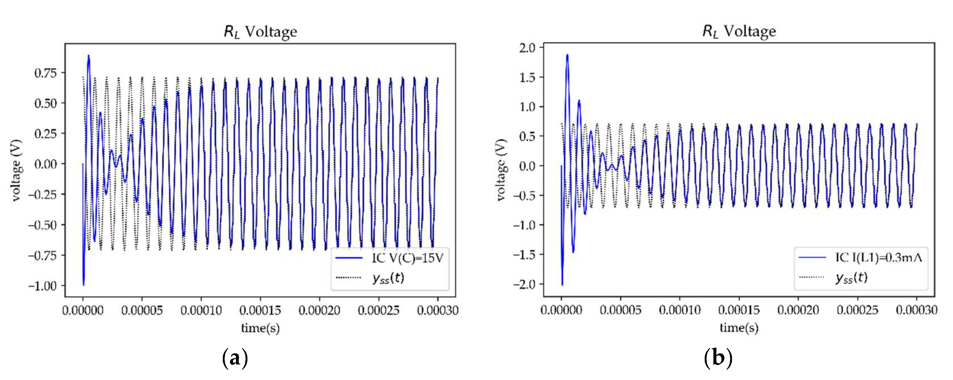
Hence, to obtain a representation from our proposed steady-state function and show the steady-state conditions from our system, we compared the
and
computations with SPICE simulations. The simulations were performed on our proposed circuit in
Figure 2b and the components were configured as in
Table 1. At this step, we calculated the frequency
and capacitor (
C) using the resonant frequency from the primary circuit described in Formula (19).
Using Formula (19), we calculated
to obtain the resonant frequency of 100 kHz. The transient analysis simulations were ran with intervals of 0–0.3 ms using a 1 V sine wave input. The simulations were configured by giving the
x(0) initial conditions a random value, which is defined in
Table 2.
We plotted the transient simulation results for the
voltage and compared them to the
model in
Figure 3. The first setup results represented in
Figure 3a show the unsteady
voltage when the initial condition of 15 volts is given to the capacitor. The
voltage begins to steady after 0.1 ms. When the 0.3 mA initial condition is given to
(setup 2), the unsteady behavior occurs at the beginning from 0 to 0.9 ms, as shown in
Figure 3b. Results from
Figure 3 show that, under the steady-state condition, the
model gives similar values compared to the simulation. Therefore,
is a stable solution.
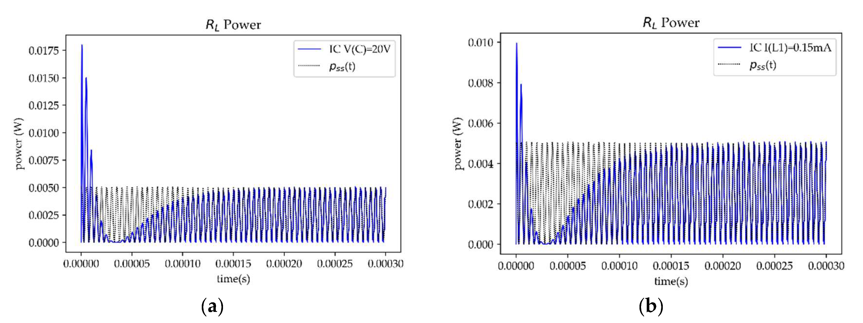
The comparison of
with the SPICE transient simulation result is presented in
Figure 4. The initial condition given to the capacitor (setup 3) and
(setup 4) generates unsteady behavior at the beginning of the simulations. However, when the time reaches 0.3 ms, the simulation result shows that the system began to reach the steady-state condition, and it has similar outputs with the
calculations. Therefore, the steady state’s average power calculations can be obtained using
, since this function shows the stable solution.
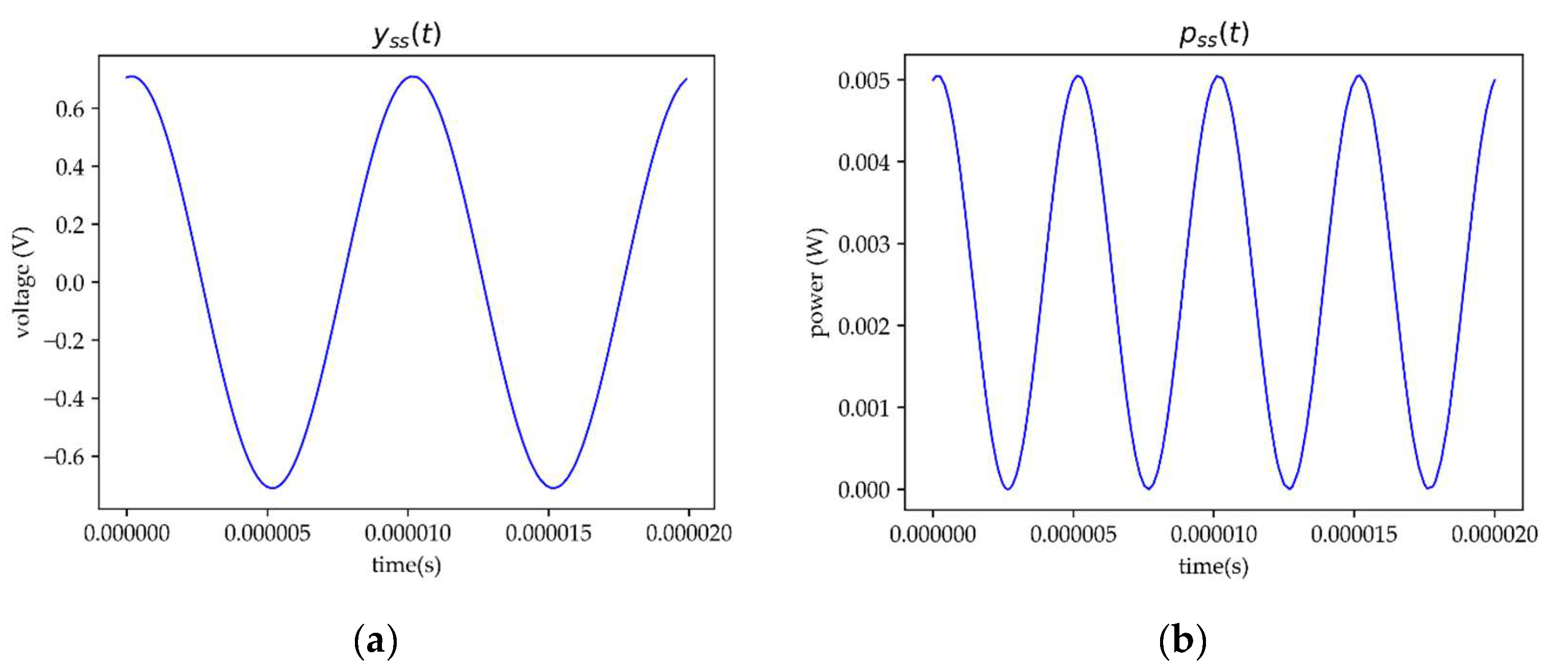
3.2. Comparison of Average Power at the Load between the Unoptimized and the Optimized Capacitor Frequency Values
This section compares the unoptimized and optimized average power calculations for our single-capacitor circuit, shown in
Figure 2b. First, the component value is set using the values in
Table 1. Then, for the unoptimized condition, the capacitor and frequency values are calculated using the primary-side resonant frequency from Formula (19). Therefore, we obtained
and the frequency 100 kHz. Then, using Equations (8) and (9), we computed and plotted
and
in
Figure 5. From Equations (10) and (11), the average power calculations were obtained as 2.5 mW.
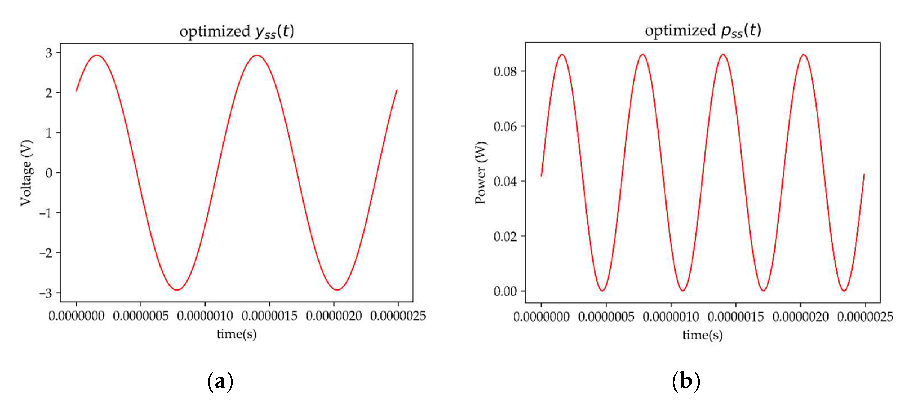
Next, we optimized the capacitor and frequency values (
C–
f) using our proposed method to obtain
and
as in Equations (15) and (16). The calculation shows that
rad/s. From
, the frequency was obtained at 803.6 kHz. Afterward, we substituted the
value into Equation (15) to obtain
=
, since
as mentioned in Equation (13), and
. Then, the
C value was found to be equal to 1.56 nF. Using this optimal
C–
f value, we computed and plotted
, and
, as presented in
Figure 6. The average power obtained from the calculations of Equations (10) and (11) was 0.043 Watts. By comparing the unoptimized condition in
Figure 5 and the optimized condition in
Figure 6, we determined that the load’s average power
improved significantly after
C–
f was optimized.
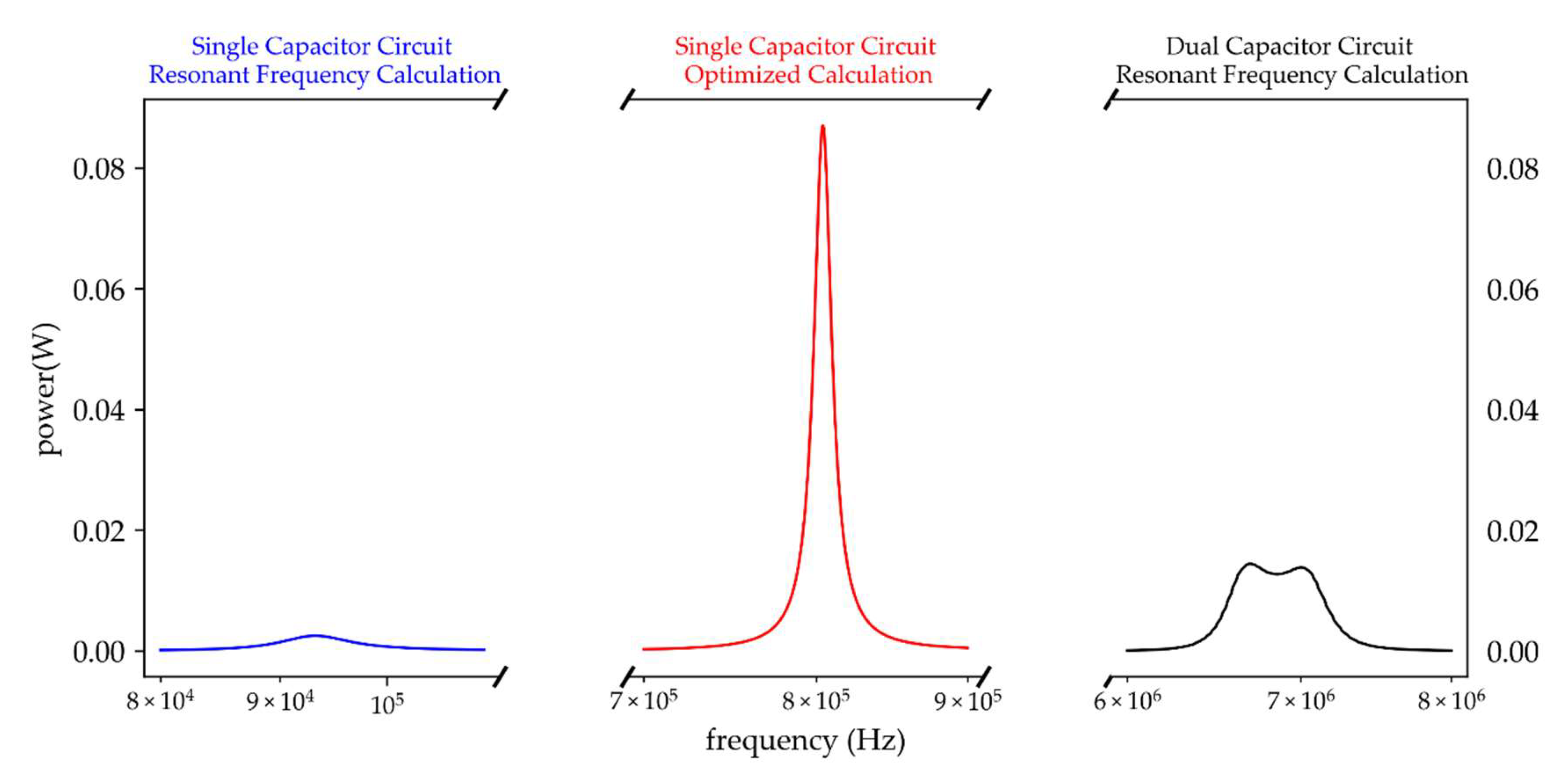
3.3. Comparison of Power at the Load between Optimized Single-Capacitor and Dual-Capacitor Resonant Calculations
To verify that our proposed design method can obtain a high-power level that is high enough compared to the resonant calculations (even if the circuit loses symmetry and not using the idea of resonance), we performed SPICE simulations using the scenarios as follows:
Single-capacitor WPT circuit (
Figure 2b) using the idea of primary-circuit resonance for
C–
f from Equation (18).
Single-capacitor WPT circuit (
Figure 2b) with an optimized
C–
f condition using the proposed Formulas (15) and (16).
Common dual-capacitor WPT circuit (
Figure 2a) using the idea of primary-circuit resonance for
C–
f from Equation (12).
The SPICE simulation uses each circuit’s environment setup, shown in
Figure 2, and the fundamental component values, presented in
Table 1. Since our proposed formula in scenario 2 introduces new variables, we converted the component values in
Table 1 into those presented in
Table 3 using Equation (13). At the same time, the
C–
f method calculation for each scenario is described in
Table 4.
After calculating each configuration’s capacitor and frequency (
C–
f), we ran the SPICE AC analysis simulation.
Figure 7 presents the results of the SPICE small-signal AC analysis. From these results, we can verify that our proposed design method for a single-capacitor circuit using the proposed optimized
C–
f is able to obtain a high enough power level compared to that of the common dual-capacitor circuit using the idea of resonance. Furthermore, our proposed formula for obtaining an optimized
C–
f can be used even if our single-capacitor circuit loses symmetry and does not use the idea of resonance.
3.4. Optimization during Changes in the Coupling Coefficient (K)
In this section, we conduct
C–
f optimization while the coupling coefficient (
K) changes, simulating distance variations between coils [
16]. Our proposed optimization maintained a high-power level, which we verified by performing the
C–
f computation in conjunction with the changes in
K using the SPICE simulations. We used all the circuit component values from
Table 1 except
K, which we set as a free variable. Next, we compared the fixed
C–
f (
C = 1.56 nF and
f = 803.6 kHz) with the optimized
C–
f when the coupling coefficient
K is swept from 0.03 to 0.5. Finally, we computed the optimized
C–
f using Equations (15) and (16) and observed the results, presented in
Figure 8. The fixed
C–
f demonstrates power degradation as
K increases. However, the optimized
C–
f maintains the optimal power level, starting when the
K coupling coefficient is larger than 0.1.
The verification of the optimization conducted via the SPICE simulation using
K’s value is shown in
Table 5. We ran the simulations of AC analysis using the linear time sweep with 1000 points and computed the optimized
C–
f value results, which are shown in
Table 5. The simulation plot is presented in
Figure 8b. As shown in
Figure 8a, power degradation occurs when
K is between 0.1 and 0.2, and it further decreases when
K reaches 0.5. However, when the
C–
f is optimized, the
power shows a stable 0.14 Watt result.
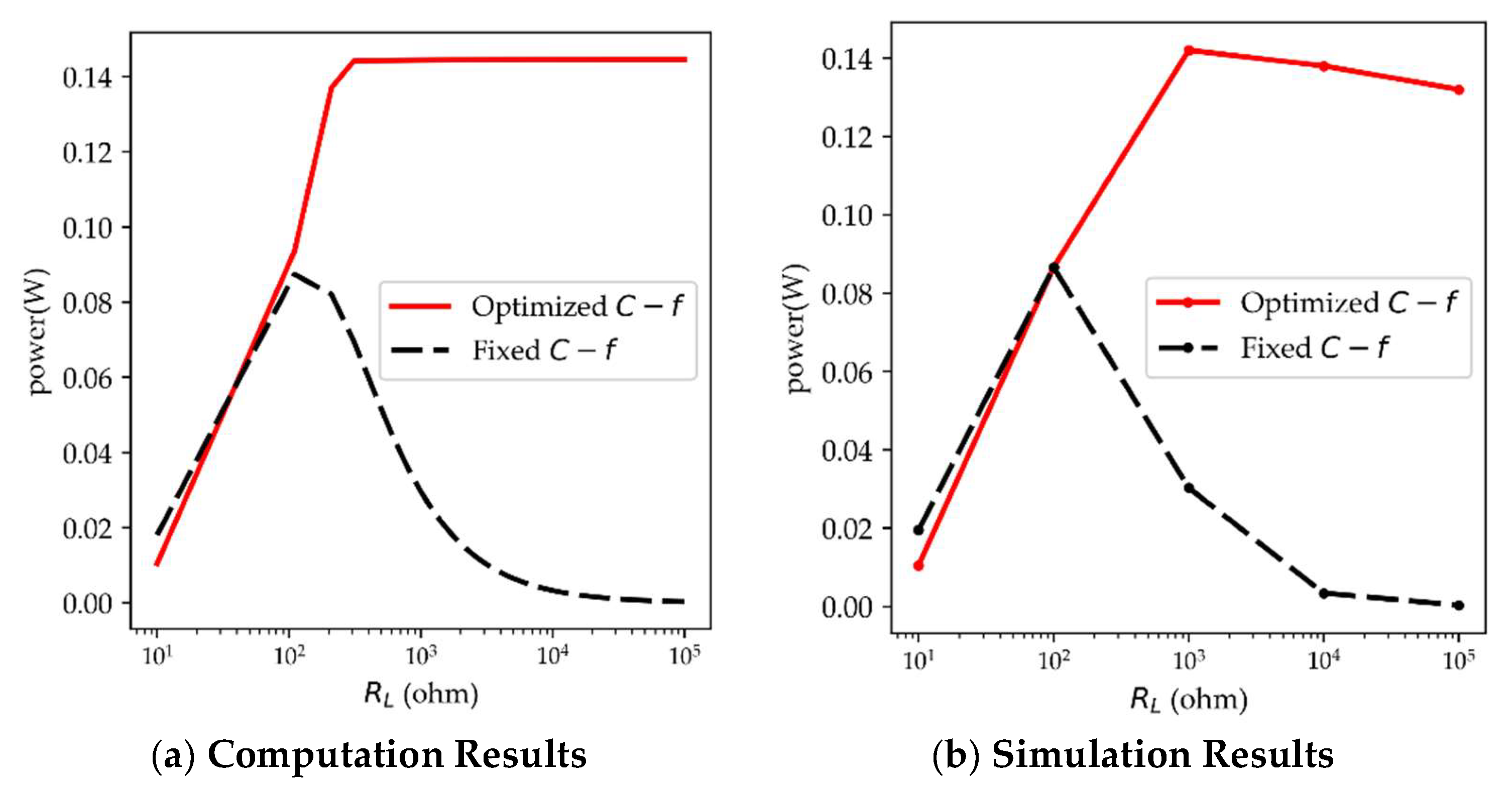
3.5. Optimization during Changes in Load ()
This section aims to verify our proposed optimization under different types of loads by observing the optimization results during changes in load (
). The optimization was performed using the topology shown in
Figure 2b and the component setup listed in
Table 1, with
being set as the free variable. To evaluate the performance of our proposed optimization, we compared the fixed
C–
f (
C = 1.56 nF and
f = 803.6 kHz) with the optimized
C–
f computed using Equations (15) and (16). The
C–
f optimization was carried out while varying
from 10
to 100 k
(with 1000 data samples), and the results observed are plotted in
Figure 9a. The computation results demonstrate that the fixed
C–
f experiences power degradation as the
increases. In contrast, our proposed optimized
C–
f shows a stable optimal result starting when
reaches 100
.
The optimization verification was conducted in the SPICE simulation environment. To evaluate the effectiveness of our proposed optimization, we observed the
power consumption while fixing the
C–
f at 1.56 nF and 803.6 kHz for different values of
, which are listed in
Table 6. The simulations were ran through the AC analysis with a linear time sweep of 1000 points. The obtained results were compared with the optimized
C–
f listed in
Table 6, and the comparison results are presented in
Figure 9b.
4. Discussion
This study was conducted in three phases to achieve a high-power level with the load
. The first phase consisted of finding the system model for the primary-side single-capacitor WPT system, which was represented using the transfer function shown in Equation (2). In the second phase, steady-state analysis was performed, and the steady-state function
power
was obtained, as shown in Equation (9). The simulations with the initial condition presented in
Figure 3 and
Figure 4 indicate that
is a stable solution. Therefore, the average power of
can be calculated using the integration formula presented in Equations (10) and (11).
Optimization was carried out to maximize
and to achieve a high-power level absorbed by
. Therefore,
was set as the objective function. This study used the partial derivation of the capacitor and frequency to obtain the optimum point
, as in Equation (15), and
, as in Equation (16). The optimum function for
power can be obtained by substituting
and
into the objective function. A contour map is presented in
Figure 10 to show a better perspective of the optimization results. In
Figure 10, many peaks can be observed around the selection value for the capacitor and frequency. The
power obtained from the primary-circuit resonance frequency
C–
f is far smaller than that from the optimized
C–
f.
This study compared the optimized
C–
f results with: (1) the single-capacitor primary-side resonant frequency calculation, and (2) the dual-capacitor circuit with the resonant frequency calculation. The comparison results show that the optimized
C–
f can deliver the highest power to the
, as shown in
Figure 7. Next, this study presented the optimized
C–
f system behavior during coupling coefficient
K or load
changes. The results are presented in
Figure 8 and
Figure 9. Equations (15) and (16) were used to find the extremum point
C and
f, which can be used to maintain the optimal condition during changes to the
K or
value.
Table 5 shows interesting results when the coupling coefficient
K =
0.
13. At this value of
K, the optimized capacitor calculation is 40.4 pF, and the optimal frequency is 5.032 MHz. These optimized capacitor and frequency values are considered outliers compared to the other results in
Table 5. Therefore, this study investigated further by conducting a numerical analysis using narrower values of
K. The calculation was performed using Equations (15) and (16), and the results are presented in
Figure 11a. The critical point for the frequency is calculated at 29.56 MHz when
K = 0.131. Similar situations happen during the numerical analysis with the narrower
(100
–10 k
), as presented in
Figure 11b. The critical point for the frequency is calculated at 26.47 MHz when
. Hence, these two situations are marked as important since they border the maximum power.
Figure 11 shows the high-power area; in this area, we can select any critical points of a capacitor, frequency, coupling coefficient, or load resistor to suit the required condition.
This study demonstrates that the critical point
K or
can be determined from the numerical calculations. Additionally, the critical capacitors and frequency can maintain optimal conditions during coupling coefficient or load changes, allowing for optimal solutions to be selected based on system requirements. The optimization can be improved in future research by utilizing Equations (15) and (16) to obtain the critical values of the capacitor and frequency; then, constrained optimization techniques can be applied, such as the Karush–Kuhn–Tucker conditions [
37], to satisfy the system requirement regarding the constrained condition in the frequency, capacitor, coupling coefficients, or load.


