Article

Integration of Sodium Metal Halide Energy Storage Systems in Telecommunication Microgrids: Performance Analysis of DC-DC Converter Topologies

1
Department of Electrical and Electronic Engineering, University of Cagliari, Via Marengo 2, 09123 Cagliari, Italy
2
Department of Information Engineering, University of Florence, Via S. Marta 3, 50139 Firenze, Italy
*
Author to whom correspondence should be addressed.
Energies 2023, 16(5), 2169; https://doi.org/10.3390/en16052169
Submission received: 21 December 2022 / Revised: 13 February 2023 / Accepted: 20 February 2023 / Published: 23 February 2023

Abstract

:
The present paper proposes an integrated method for modelling and designing Energy Storage Systems (ESSs) based on Sodium Metal Halide Batteries (SMHBs). The implementation of the proposed methodology for designing an SMHB-ESS used for supporting telecommunication DC microgrids is presented. The motivation concerning this specific case study is the role assumed by battery technology in improving the reliability and robustness of telecommunication DC microgrids. In this context, the SMHBs, due to their operative temperature, dynamic power response and robustness against cell breakdown, represent one of the most suitable technologies, mainly when challenging environmental conditions occur. The motivation for implementing an integrated design approach is the non-linear behaviour of SMHBs, which requires a high accuracy in battery modelling and in managing DC-DC interfacing for full SMHB capacity exploitation. To highlight the advantages of this novel approach, a comparison between the SMHB- ESS designs considering, as the DC-DC converter, a buck–boost topology actually implemented in the commercial systems and a Dual-Active-Bridge (DAB) converter, specifically developed for this kind of battery, was investigated. Considering different operating conditions in a specific DC telecommunication microgrid, the designed configurations of SMHB ESSs were simulated. Finally, a comparison of simulation results is presented and discussed, highlighting that DABs, despite their greater complexity compared to buck–boost converters, present advantages in terms of flexibility, dynamic performances and efficiency, increasing the available SMHB capacity by 10%.

1. Introduction

The worldwide demand for information and communication technologies has registered exponential growth in the last few years, resulting in an increasing request for telecommunication infrastructures. Specifically, telecom companies have developed tailored solutions to guarantee a reliable communication system able to cover areas unserved by power systems and characterised by prohibitive locations and challenging weather conditions. The solutions actually implemented allow for the supply of telecommunication equipments both in islanded or grid-connected configurations. In particular, the classification of telecom power systems highlights that most of them can be included in the cluster of DC microgrids. In this case, the telecommunication devices are interfaced with each other, complying with specific DC standards. In this context, the energy storage systems (ESSs) assume a fundamental role because they assure the stabilisation of DC microgrids, the reinforcement of power quality in the presence of unpredictable variations in the demand/supply, and reliability during power system outages. At present, the ESSs implemented in DC telecommunication microgrids are based on electrochemical batteries. Currently, the battery technologies used in these applications are mainly lead–acid and lithium-ion batteries [1,2,3,4,5]. One of the most promising electrochemical technologies for ESSs in DC telecommunication microgrids is Sodium Metal Halide Batteries (SMHBs). They can provide short-time and high-peak-power pulses at any operating state of charge (SoC) [6,7]. Moreover, they are independent of climatic conditions due to their high inner operative temperature. Another specific feature is the sodium metal halide cells’ capability to work under short-circuit conditions. This property allows for bypassing the faulty cell using itself as a short circuit, preserving the battery string functionality and reliability of the ESSs. Furthermore, recent studies [8] have shown that, by accurately modelling SMHBs, it is possible to fully exploit the available capacity concerning previous models [8,9]. In fact, the non-linear behaviour of SMHBs makes the battery energy management challenging at SoC values lower than 30% when standard electrical models are used. This is due to the iron doping of SMHBs, which increases the battery power density and power pulse response but introduces significant non-linearity for SoC values lower that 40%. For this reason, the available SMHB capacity in commercial products is limited to safely performing battery management, fixing the minimum SoC value in a range between 40–20%. The electrical modelling reported in [8] overcomes this issue by reconstructing iron doping effects and allowing for an accurate mimicking of SMHBs voltage evolutions for any load condition until an SoC of 10%. This solution opens new opportunities for increasing the available capacity in SMHBs and detecting cell faults at any SoC value. The implementation of the advanced modelling also implies the possibility of increasing the operative battery capacity or reducing the number of cells per string concerning that commonly installed in SMHBs for telecommunication applications, keeping the operating ESS capacity unchanged. However, to fully exploit the SMHB potential in ESSs, particular attention must be addressed to the DC-DC converter used to interface the SMHB. Specifically, it has to be characterised by a high flexibility, accuracy in managing battery voltage and current and tailored control based on the SMHB modelling. Moreover, the management of power flow between ESS and microgrid requires the battery charging and discharging, imposing the implementation of a bidirectional DC-DC converter. In this context, a novel design approach aimed at integrating advanced SMHB modelling to improve the energy performance of SMHB-ESSs for DC telecom microgrids is proposed. Regarding the electrochemical battery, the developed modelling and the analysis refer to a commercial SMHB module produced by the FZSoNick (model 48TL200) for telecommunication applications. The management of the telecom SMHB refers to the advanced modelling experimentally validated and reported in [8]. Regarding the DC-DC converter, various topologies for energy storage applications have been proposed. The buck-boost converter is one of the most popular converters in ESSs due to its simple structure and high efficiency. Moreover, it can be implemented in a wide range of powers, resulting in an interleaved configuration.For ESS applications requiring a high voltage and isolation, the transformer-based converter being a flyback or push–pull converter can be a suitable solution. However, these converters lead to heavy and oversized structures with a lower efficiency than buck–boost converters due to the higher number of middle blocks and components used. The cascaded converters are suitable for high-gain approaches, and since there is only one switch per block, the control process is simple. Although their gains are highly achievable, cascaded converters present a low efficiency, especially for high serial numbers blocks. The switched-capacitor (SC) and switched-inductor-based (SI) DC-DC boost converters overcome the above-mentioned issues. Another type of DC-DC boost converter is the coupled-inductor-based converter. Although the number of turns in the inductor is an essential parameter for determining the converter’s voltage gain, the input current levels increase by enhancing the number of turns, which causes high-level input currents with large ripples that will impact the long life of the inductor and input capacitor [10,11]. Among these topologies, the authors have focused their attention on the bidirectional buck–boost converter because it is actually implemented in the commercial systems, and on a Dual Active Bridge (DAB) because it is characterised by a simple topological structure, galvanic isolation, a large input–output voltage range, a scalable power range, a high conversion efficiency, a high power density and a dynamic performance. These features make DABs one of the most interesting DC-DC topologies for managing the power flow between the SMHB and microgrid [12,13,14,15]. Defining the bidirectional DC-DC converter topologies under evaluation, an integrated design methodology suitable for implementing an advanced SMHB model in ESSs for fully exploiting the SMHB capacity was developed and implemented. In particular, a configuration of SMHB-ESS characterised by a lower number of cells per string with the same operative capacity as the commercial one was designed. This solution represents a significant competitive advantage because it allows for the achievement of the same performance at a lower cost and represents the application fallout of the proposed activity. To verify the performance and demonstrate the feasibility of using the proposed SMHB-ESS in DC telecom applications, a design was developed considering an SMHB whose string has 16 cells connected in series instead of 18 and a rated battery voltage of 39 V instead of of 46.5, with an operating capacity range of 90–10% and an output rated voltage of 48 V. The design specification requires that the converters and the filtering elements allow the buck–boost operation to operate in continuous conduction mode and the DAB to operate in Zero Voltage Switching (ZVS) in wide operating conditions. Regarding the control system, a feed-forward control algorithm based on SMHB modelling was synthesised in order to perform a comparative analysis between buck–boost and DAB converters that is not influenced by the specific feedback control techniques implemented. The paper is organised as follows: the standards for telecom applications is firstly introduced, and then the typical operation of an SMHB and its modelling is presented. Subsequently, bidirectional DC-DC converters topologies are analysed. Finally, the topologies and control strategies are presented by extensive simulation studies in the MATLAB/Simulink and SimPowerSystem environment, and the results obtained are compared and discussed.

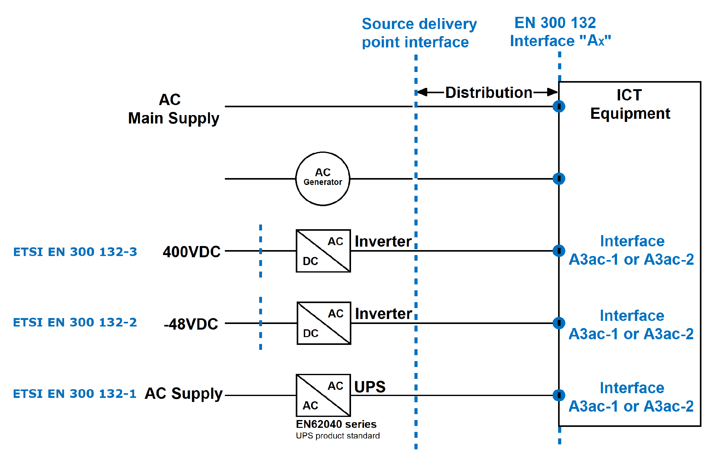
2. Telecommunication Standards

The system under analysis comprises an SMHB coupled to the telecom DC microgrid through a DC-DC converter. In order to define the design specifications, it is important to summarise the standards related to telecommunication systems. The reference regulatory framework is reported in “ETSI EN 300 132” [16,17,18]. It is composed of three parts that define, for specific cases, the electrical requirements of the power supply of telecom equipment at the interface. Figure 1 reports the block diagram that summarises the application voltage rating and the standard correspondent part. The first part deals with the connection standards in the case of an AC network supply, the second one refers to the 48 V DC network and the third one considers the standards in the case of a supply voltage of 400 V DC.
The focus of this paper is on the part that defines the normal service voltage range and the abnormal service voltage range for the interface at the 48 VDC as reported in Table 1.
These requirements shall be verified by the power supply and the ICT equipment at the interface “ A x ”. The testing and measurement techniques are described in CENELEC EN 31000-4-29 [7]. Typically, the classification groups ICT equipment into three main categories: Ground Base Tower (GBS), Rooftop Tower (RTT) and Rooftop Pole Tower (RTP). Each tower is composed of both active and passive components. Active components consist of the Base Transceiver Station (BTS), transmitter and receiving modules, a mobile switching centre and a multiplexer. Passive components consist of antenna mounting structures, equipment housings, etc. The energy consumption of a telecommunication tower can vary considerably depending on various factors, such as indoor or outdoor installation, the number of receivers and transmitters and auxiliary loads. The technical literature reports examples of typical loads for telecommunication systems [19,20,21,22]. The proposed analysis considers a DC steady-state power demand of 2 kW.

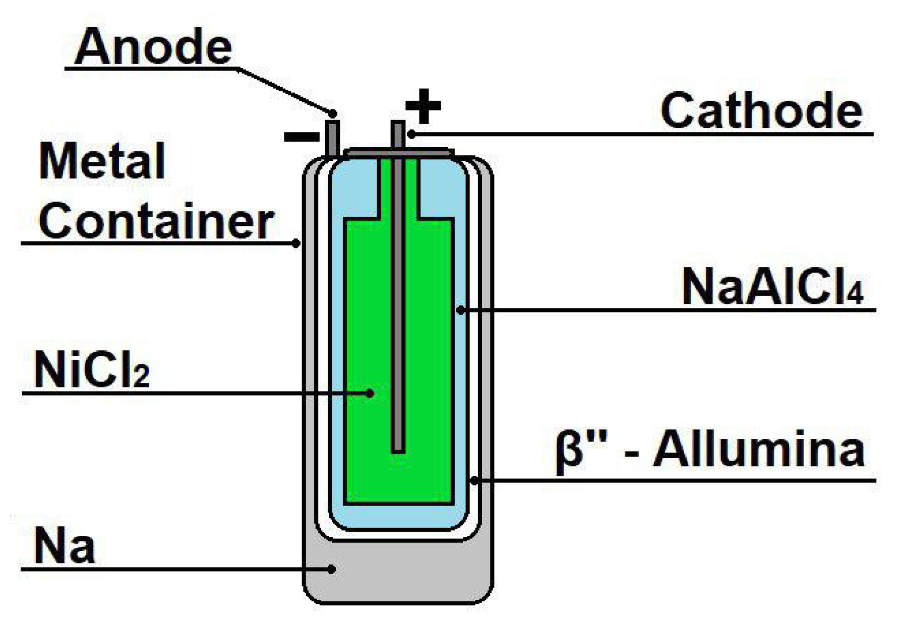
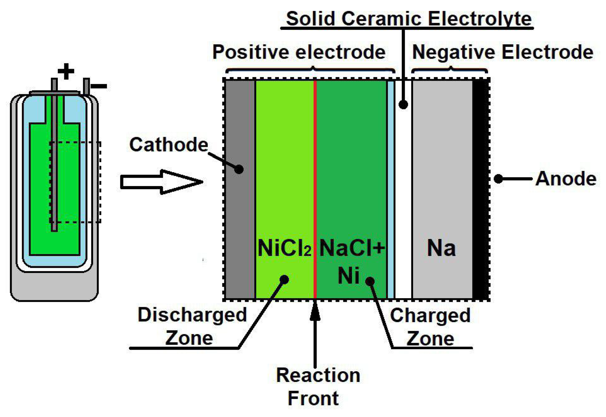
3. Sodium Metal Halide Batteries

Sodium metal halide batteries are second-generation electrochemical batteries made of available and recyclable elements. Figure 2 shows a schematic representation of a sodium metal halide cell (SMHC) with the main elements of these batteries. The cathode is composed of nickel chloride ( N i C l 2 ) and sodium aluminate tetrachloride ( N a A l C l 4 ), which promotes the flow of ions through the ceramic layer and a current nickel collector. The anode is made up of liquid metallic sodium. The ceramic layer of β -alumina guarantees the electrical insulation between the cathode and the anode, which also allows for the selective migration of sodium ions N a + that are the inner battery charge carriers, as can be deduced from (1).
N i C l 2 + 2 N a 2 N a C l + N i @ O C V n i = 2.58   V
Figure 3 shows a schematic representation of the chemical reactions inside the cell. During the charging process, sodium chloride reacts with nickel to generate nickel chloride, whereas, during the discharging phase, the nickel chloride and liquid metallic sodium react to generate sodium chloride and solid nickel. The reaction front moves away from the electrolyte when the battery is discharged, and this phenomenon determines the characteristic increase in the internal resistance for this type of battery. Doping the cathode with active iron materials increases the SMHC power density. Iron operates in the SMHC in the same way as nickel, as shown by (2), but at an Open Circuit Voltage O C V f e equal to 2.35 V.
F e C l 2 + 2 N a 2 N a C l + F e @ O C V f e = 2.35   V
The reaction that affects nickel occurs at an O C V n i of 2.58 V, which is higher than the voltage of the iron reaction (2.35 V). This electrochemical configuration makes the dynamic modelling of the SMHB a particularly complex task, especially at SoC values lower than 40%, where the SMHB voltage assumes values for which both reactions can be performed simultaneously [8].
A detailed description of the chemical phenomena occurring in the SMHB at SoC values lower that 40% is reported in [9,23].
The rated voltage of the SMHC is equal to 2.58 V. Therefore, the series connection of an appropriate number of cells allows for the achievement of specified values of rated voltage suitable for the telecommunication DC microgrid. Specifically, the proposed case study considers a microgrid DC-rated voltage of 48 V according to ETSI EN 300 132—Part 2 standard. Hence, the minimum number of SMHCs composing the SMHB string is 18.

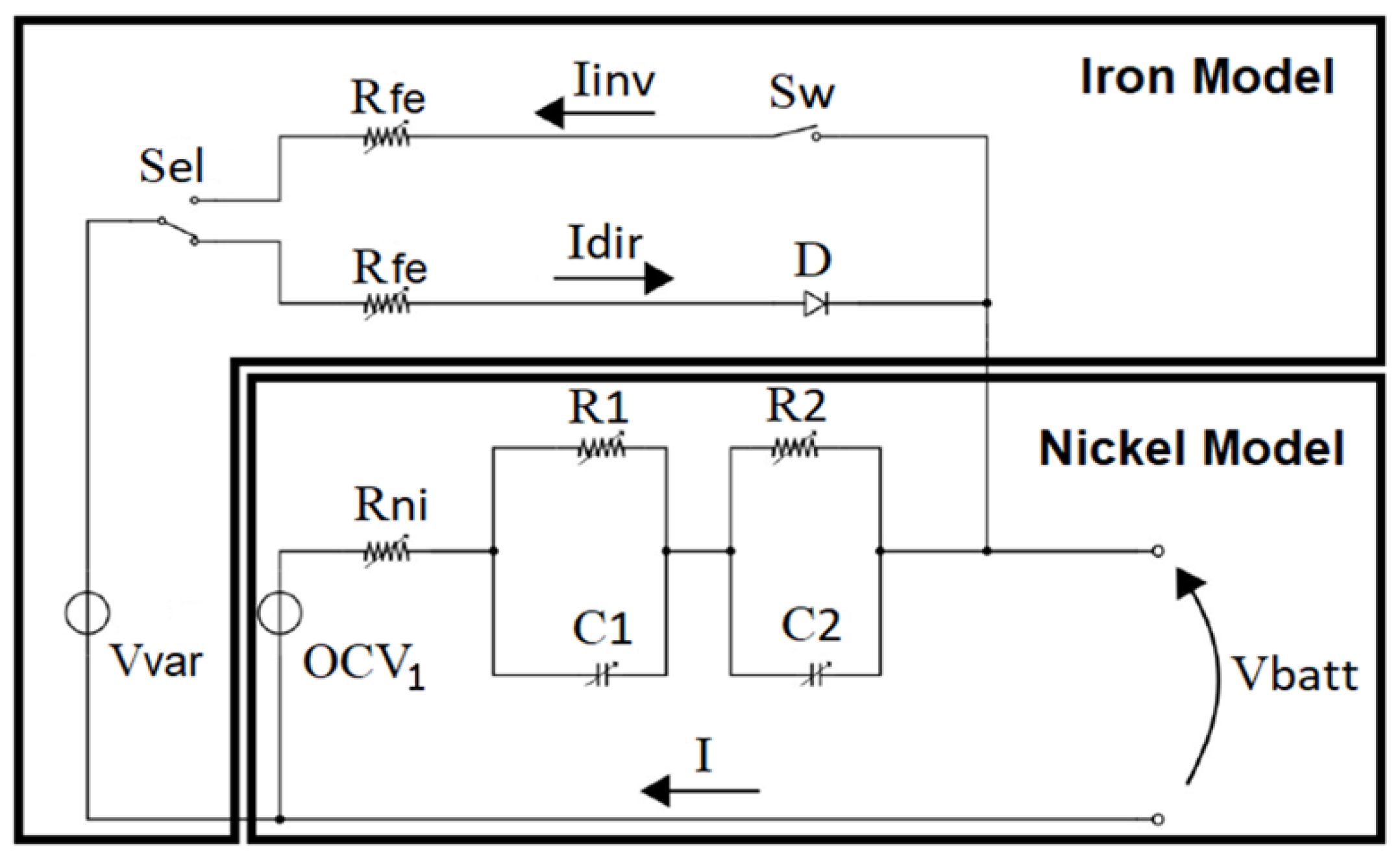
4. Electrical Model of SMHB

As reported in the previous section, the electrical modelling of SMHBs is particularly complex due to the effects associated with the existence of two different reactions occurring at the same time. This phenomenon assumes a significant relevance for SoC values lower than 40% because a higher probability of having the two reactions makes using a linear electrical model difficult. In particular, if the discharging process requires a power peak, this can cause a voltage drop that brings the SMHB voltage below the triggering voltage of both reactions.
In order to model this behaviour during charging and discharging, the standard electrical model might not be sufficient. A Thevénin equivalent circuit, shown in Figure 4, that reproduces the SMHB voltage evolution accurately was recently proposed and validated [8]. The proposed equivalent electrical circuit comprises a voltage generator, one series resistor and two RC branches. Moreover, to account for the phenomena associated with iron doping, two equal resistors representing the equivalent inner resistance of iron-based cells powered by a variable voltage generator are placed in parallel with the Thevénin circuit. The variable voltage generator depends on the battery voltage and the currents flowing in the iron resistances. The introduction of two properly managed switches allows for the accurate mimicking of the phenomena related to the iron reaction.
A more detailed description of the iron-doped SMHB model and the chemical phenomena occurring in the SMHB is reported in [8].

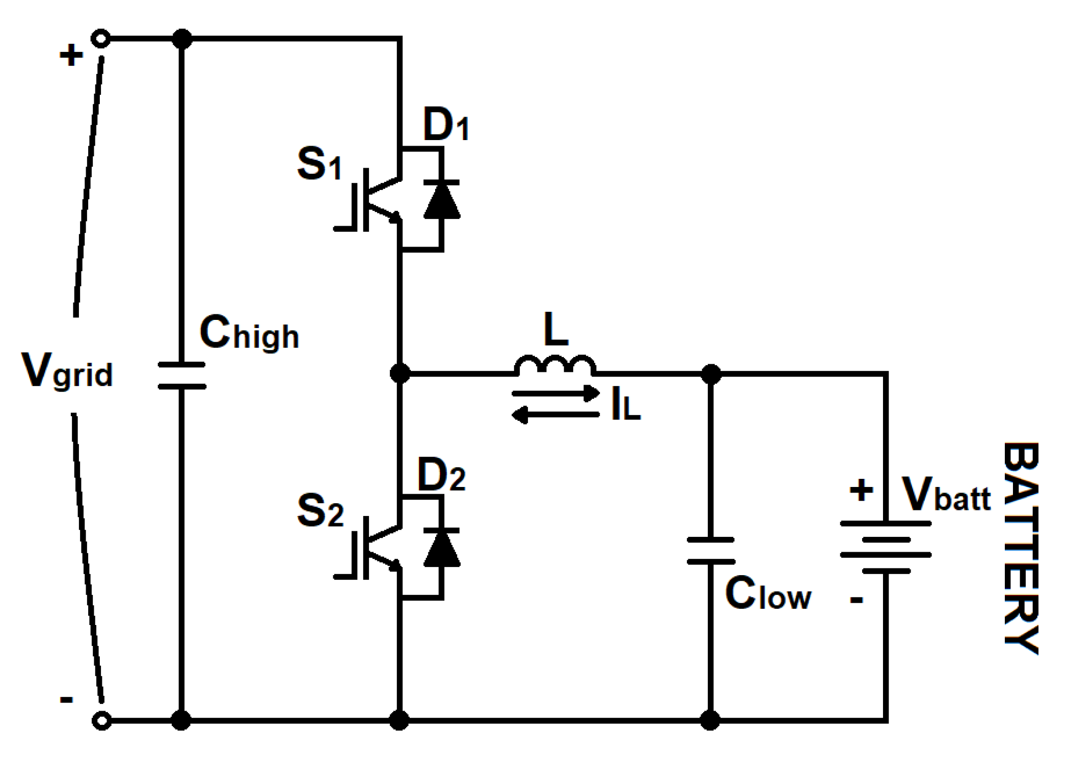
5. Buck–Boost Converter Configuration

The commercial SMHB-ESSs installed in DC telecom microgrids perform the power flow management using a buck–boost converter shown in Figure 5. This DC-DC converter allows for bidirectional power flow management, resulting in a variable-structure configuration. Specifically, the management of switches S 1 and S 2 allows the passage from the buck to boost configuration. Specifically, keeping the switch S 1 permanently off, a boost DC-DC converter supplied by the battery is achieved. The power delivered by the battery to the DC microgrid can be appropriately controlled by modulating the switch S 2 . On the other hand, keeping the switch S 2 permanently off, a buck DC-DC converter supplied by the DC microgrid is fulfilled, permitting the battery charging through switch S 1 modulation. Indeed, this kind of buck–boost converter in commercial telecom SMHB-ESSs is mainly used as a battery charger because the forward bias of the diode D 1 assures the battery supply of the DC microgrid during grid outages. This solution implies that the rated battery voltages must be within the range imposed by telecom standards. For this reason, monitoring battery voltage is mandatory to prevent the drop caused by discharging and self-discharge. Toward this aim, the buck converter has to charge the battery, imposing a controlled voltage evolution on the battery side so that the constant current/voltage mode can be imposed, according to the Battery Management System (BMS) control rules. In SMHBs, this configuration has another essential function. If faults on SMHCs occur, the control of battery string voltage compensates for the voltage drop caused by the short circuit of faulty cells. In this context, the boost mode is helpful to compensate for the reduction in the battery voltage, guaranteeing the output voltage according to the telecom standards of ESSs during discharging and in the presence of SMHC faults. Moreover, considering the possibility of better exploiting the battery’s capacity by properly controlling the discharging process, the boost DC-DC converter can be used to decrease the number of cells per string, consequently reducing the cost. For this reason, the design and analysis reported in the paper were performed considering a rated battery voltage of 39 V corresponding to a number of cells per string in an SMHB equal to 16. This means that the number of cells is reduced by 10%.

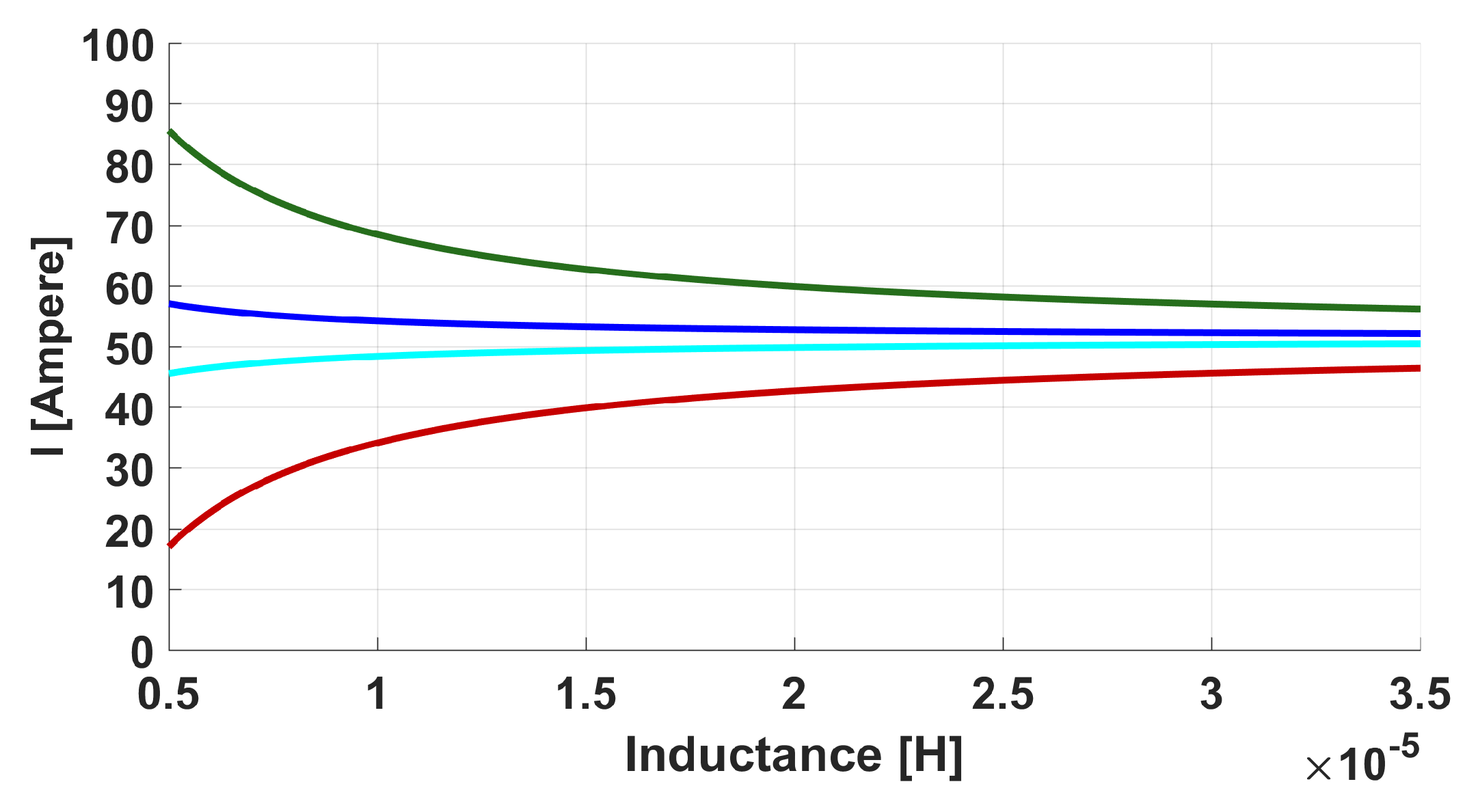
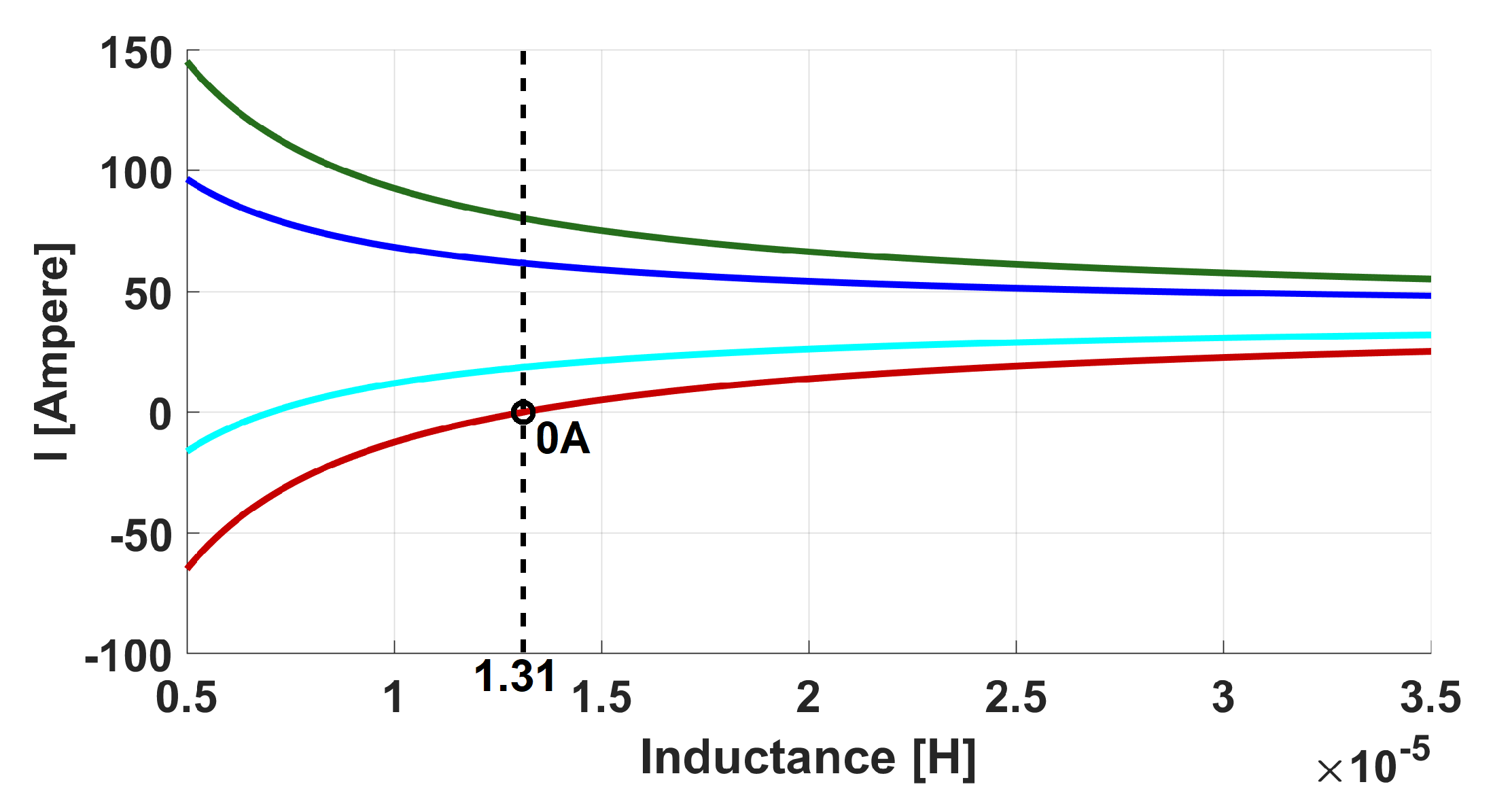
Design of the Buck–Boost Converter for Proposed SMHB-ESS

The design of inductance L has to guarantee a continuous conducting mode (CCM) in a wide operative range. Typically, the inductor current of the buck–boost converter goes from the positive to the negative direction and then swings back. Consequently, the inductor selection must keep the current positive in operative conditions. Equation (3) shows the well-known relation among the peak inductor current I p e a k , the minimum inductor current I m i n and the input and output voltage V i n e V o u t [24]. This results in:
Δ I = 1 2 V i n V o u t L V o u t V i n T s I l o a d = P o u t B B V o u t I p e a k = I l o a d + Δ I I m i n = I l o a d Δ I
where Δ I is the inductor current ripple, I l o a d is the load current, T s is the switching period and P o u t B B is the buck–boost converter load power. Assuming that the battery voltage is equal to V b a t t = 39 V and the DC-DC output voltage on the network side ranges between V g r i d = 40–50 V, during the buck mode operation and V g r i d = 50–57 V during the boost mode, it is possible, using Equation (3), to evaluate the evolution of the maximum and minimum current concerning the inductor size. Figure 6 and Figure 7 show the maximum and minimum currents vs. inductance for the buck and boost mode, respectively, referring to a power demand equal to 2 kW and a switching frequency of 25 kHz.
It can be observed that the inductance must be greater than 13.1 μH to guarantee a positive inductor current in the defined operative conditions. The low-voltage side capacitor was designed considering a low pass filter with a cut-off frequency 40 times smaller than the switching frequency.
f c = 1 2 π L C l o w
Analogously, the high-voltage side capacitor was designed in order to limit the output voltage ripple in accordance with Equation (5). Assuming V g r i d = 50 V, in the middle of the range disposed by the standards, and the duty cycle D equal to 0.78, C h i g h is equal to 1.75 mF with a voltage ripple of 5 volts.
Δ V g r i d = V g r i d R D T s C
In Table 2, the main parameters of the designed buck–boost converter for the proposed configuration of the SMHB-ESS are reported.

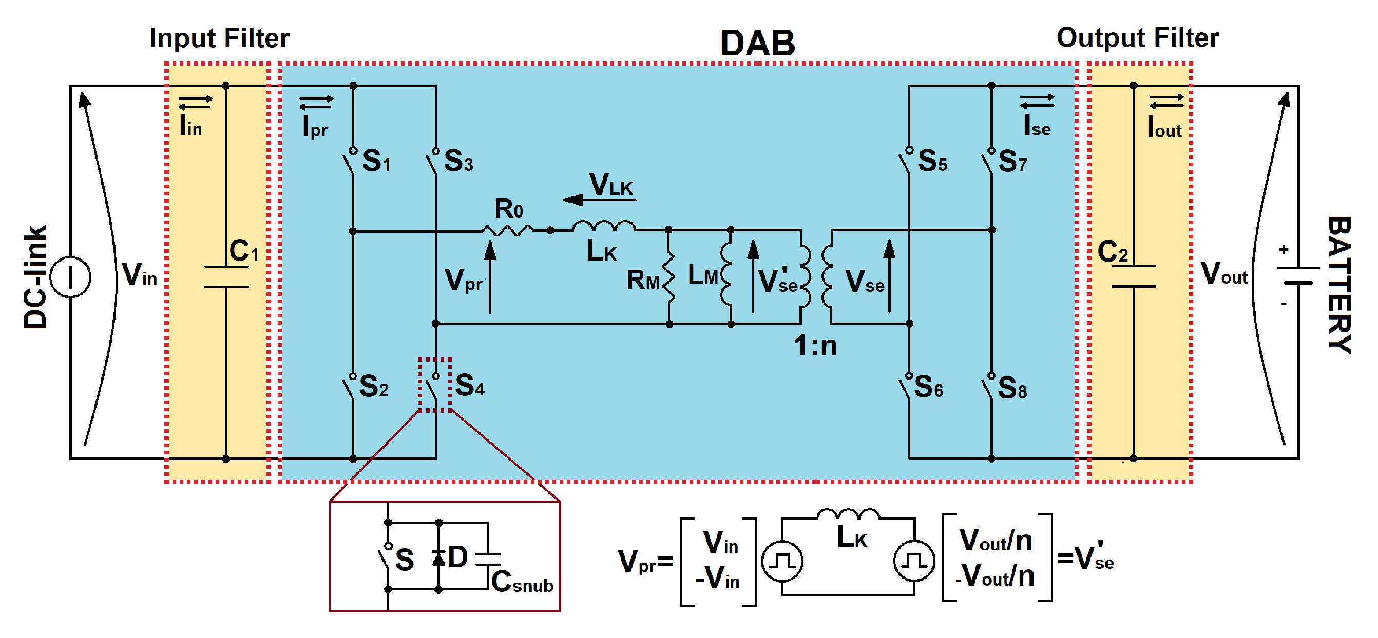
6. Dual-Active-Bridge Converter Configuration

The dual-active-bridge converter is composed of two H-Bridges coupled by a medium/ high-frequency transformer as shown in Figure 8. Typically, the modulation signal of the two H-bridges has a duty cycle equal to 50% in order to generate medium/high-frequency square wave voltage on the transformer. By appropriately controlling the phase shift between the voltage at the primary and secondary side, it is possible to control the bidirectional power flow. In particular, if the voltage at the secondary winding of the transformer lagged concerning the voltage on the primary side, the power is delivered to the battery, whereas, if the voltage at the primary side lagged concerning the secondary side, the power flows towards the grid (battery discharging).
The phase-shift modulation strategies are widely implemented to control the power flow through the DAB converter. Single-Phase Shift (SPS) [25,26,27], Double-Phase Shift (DPS) [28,29,30] and Triple-Phase Shift (TPS) [31,32] are the most used.
In this paper, SPS and and TPS were considered. The single-phase shift regulates the bidirectional power flow controlling the delay between the voltages at the primary and secondary side of the converter. In particular, the modulation signals of switches S 1 , S 2 , S 3 , S 4 and of S 5 , S 6 , S 7 , S 8 are managed in accordance with (6) in order to obtain the desired power flow. Specifically, the output power P o u t D A B can be expressed as:
P o u t D A B = V p r V s e 2 n f s w L k · D 1 1 D 1
where f s w is the switching frequency, V p r and V s e are the voltage at the primary and secondary side of the transformer, respectively, L k is the transformer leakage inductance and D 1 is the phase shift between the modulation signals of bridges connected to the primary and secondary winding of the transformer, respectively.
Compared to the SPS, the TPS introduces two degrees of freedom. In fact, TFS manages the phase shifts between the switches S 1 and S 4 and between the switches S 5 and S 8 . In this manner, the TPS improves the converter performance by reducing the current stress on the L k . Due to three degrees of freedom, there are 12 different operating modes for TPS, each having its relation between the phase shifts and the transmission power [31]. The standard waveforms for SPS and TPS are shown in Figure 9A,B, respectively.

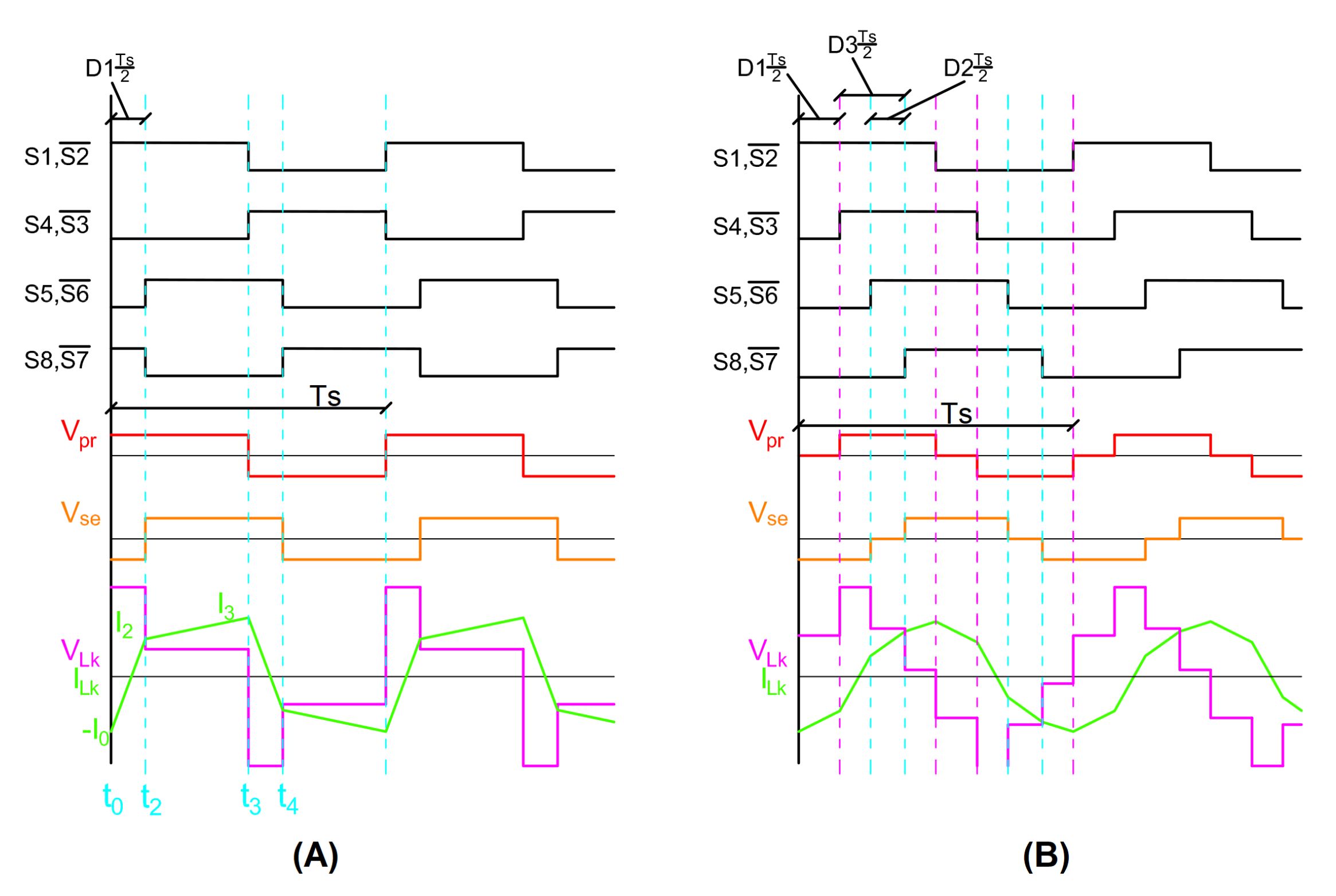
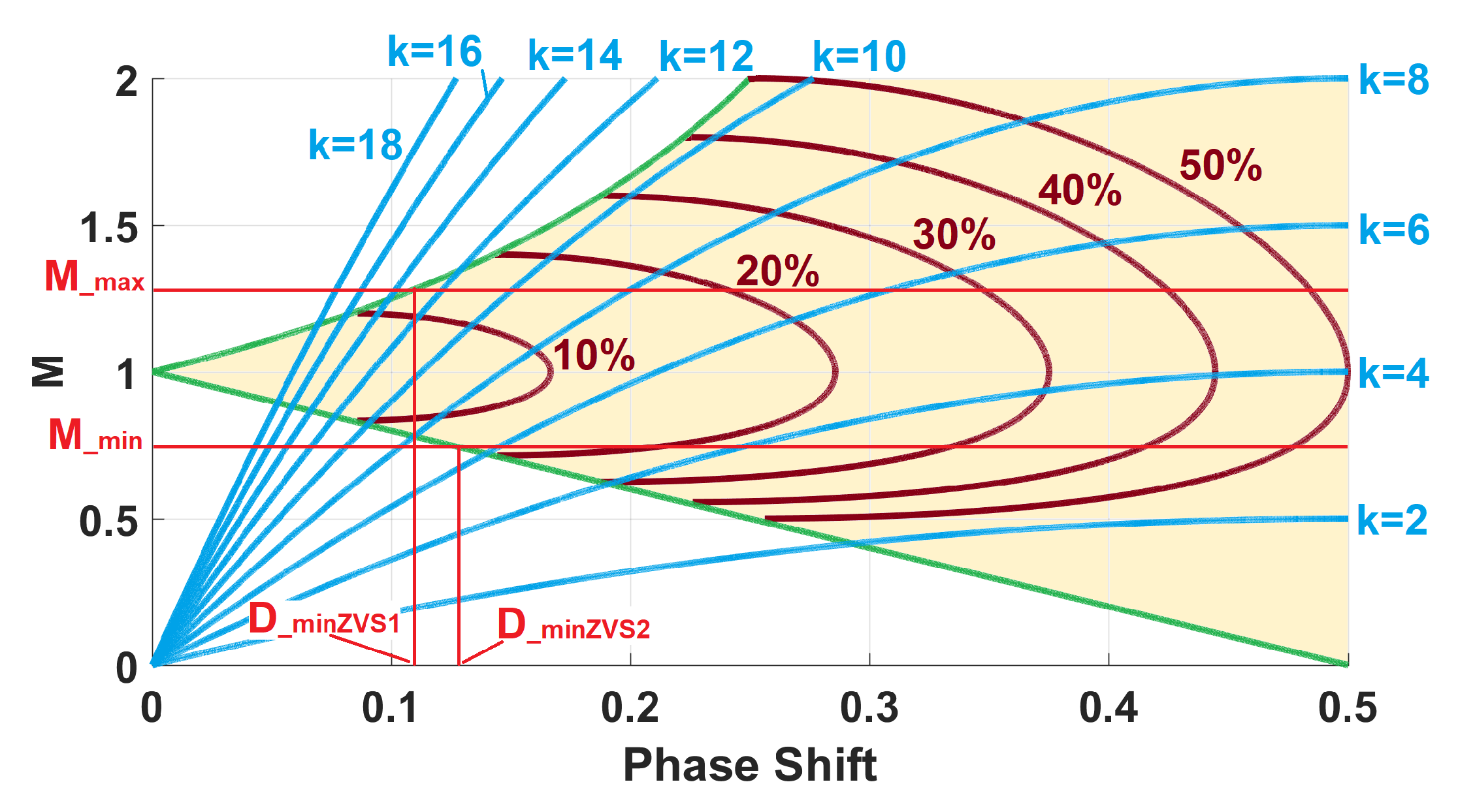
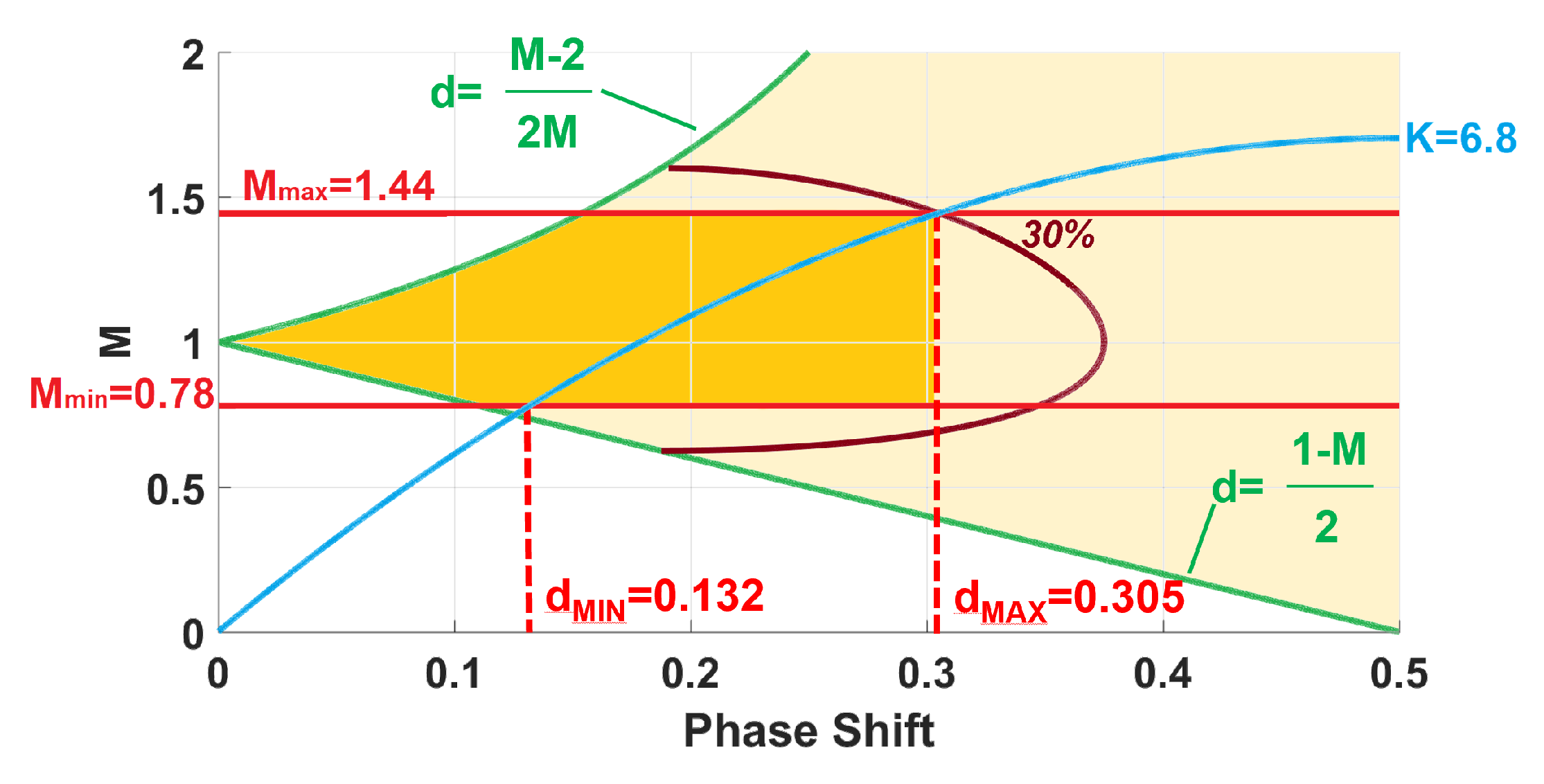
6.1. Design of the DAB Converter for Proposed SMHB-ESS

The DAB design procedures reported in the scientific literature aim to define the main hardware parameters considering the application specifications and the design targets. Specifically, the implementation constraints define the input and output voltage operative range and the rated power. On the other hand, the optimisation target addresses the evaluation of leakage inductance L k , switching frequency f s w and the operative range of phase shift D 1 to optimise specific DAB performances. Different DAB design approaches have been proposed, aiming at: increasing the efficiency at full load; extending the ZVS operation range; optimizing the current stress behaviour [33,34]. In the present paper, the DAB design was performed by referring to SPS modulation and considering the optimisation of the current stress as design criteria. Subsequently, the ZVS operation range at full load, considering the range of variation in the input and output voltages, was evaluated.
One of the methodologies for identifying the ZVS area is in [35]. It defines the operating condition in which ZVS occurs, referring to the DAB phase shift and the voltage gain. By analysing the waveforms shown in Figure 9A, it is possible to note that the conditions that the converter must respect during the charging phase are those reported in (7).
I L k t 0 = I 0 < 0 I L k t 3 > 0 ; f s w = 1 / 2 T ; V p r = V i n ; V s e = V o u t / n ; I L k t 2 = I 2 = V p r L k · D 1 · T V p r V s e 2 · L k · T > 0 ;
where T is the switching period, V p r and V s e are the voltage at the primary and secondary side of the transformer, respectively, L k is the transformer leakage inductance, I L K is the leakage inductance current and D 1 is the phase shift. Analogously, during battery discharging, the conditions are expressed as (8):
I L k t 0 = I 2 > 0 I L k t 3 < 0 f s w = 1 / 2 T ; V p r = V i n ; V s e = V o u t / n I L k t 2 = I 0 = V s e L k · D 1 · T V p r V s e 2 · L k · T < 0 ;
Solving this equation, it is possible to find a relation between the phase shift and the converter voltage gain defined as M = V i n / n V o u t and reported in (9):
D 1 1 M 2 F o r M < 1 C h a r g e D 1 M 1 2 M F o r M 1 D i s c h a r g e
Equation (9) define the boundary of the ZVS as a function of the phase shift and M but do not consider other design parameters such as loads, the switching frequency and circuit parameters. In order to introduce this aspect, it is necessary to evaluate the phase shift limits under particular load conditions that minimise the reactive component on the output current. For this purpose, the relation that links the phase shift to the circuit parameters is introduced in (10), where the term k = T R / 2 n 2 L k takes into account the load conditions.
M = V s e n V p r = D 1 · 1 D 1 · k
Furthermore, the reactive component on the output current can be evaluated by means of Equation (11) [35]
λ = 2 D 1 1 + M 2 8 d 1 D 1 1 + M + [ 2 D 1 1 M + 1 ] 2 8 D 1 1 D 1 1 + M M
where D 1 is the phase shift and M is the voltage gain as defined in (10). Figure 10 shows the ZVS zone with respect to M and D 1 . Moreover, the loci on plane M- D 1 characterised by a constant value of k (blue curves) and constant value of λ (red curves) are reported.
In the case under evaluation, the DAB parameters are the DC-link bus voltage V i n , battery voltage V o u t , transformer turn ratio n, inductance L k (including transformer leakage inductance) and switching frequency f s w . Regarding the definition of DC-link bus voltage V i n , it is characterised by a range of variations defined by telecom standards and by the voltage drop occurring on the distribution line of the DC microgrid. Hence, a minimum input voltage value V i n m i n occurs during charging at rated power. Similarly, the maximum input voltage V i n m a x during the discharging condition at rated power appears. In the same manner, the battery voltage assumes minimum V o u t m i n and maximum V o u t m a x values according to the state of charge and the battery current magnitude. The battery model allows for an evaluation of the defined number of cells of the voltage range boundaries. Defining the rated power P r as an input design parameter, (6) highlights that the DAB design has to be robust to input and voltage variations, assuring a rated power delivery. Hence, the relation reported in (12) has to be satisfied [36]. Considering the values of input and output voltages, the transformer turn ratio n was assumed to equal one. The switching frequency was set to 25 kHz. Employing these assumptions, the evaluation of DAB inductance L k can be achieved by implementing the minimisation of current stress design criteria. Firstly, an estimation of the optimal phase shift D 1 o p t that achieves the minimum peak current on the transformer at rated power and minimum input voltage can be performed referring to (13), where M m a x = V o u t m a x / V i n m i n . Consequently, the DAB inductance L k can be calculated by using (14). The methodology mentioned above was implemented, referring to the maximum output and minimum input voltages occurring on the DAB. Specifically, the M m a x and M m i n assume the values of 1.44 and 0.78, respectively. The application of (13) and (14) allows for an evaluation of D 1 o p t and of the DAB inductance L k , achieving values equal to 0.298 and 3.4 μ H, respectively. To evaluate the operating condition at a full load regarding ZVS, the operative points on the plane M- D 1 were determined and are reported in Figure 11 using the procedure previously described. The blue trace represents the working conditions at a full load for M, varying between its maximum and minimum value. The parameter k = T R / 2 n 2 L k for a defined DAB design depends on just R, which represents the load condition. The parameter k assumes a rated power value of 6.8. The results highlight that the designed DAB at rated power works in the ZVS condition, minimising the current stress. The results of the DAB design procedure are summarised in Table 3.
V i n m i n V o u t m i n 2 n f s w L k = P ^ m i n P r
D 1 o p t = 1 M m a x + M m a x 2 1 2
L k = V i n m i n V o u t m a x D 1 o p t ( 1 D 1 o p t ) 2 n f s w P r

6.2. Design of the DAB Transformer

The definition of DAB specification in terms of the leakage inductance, power rating and switching frequency allows for the design of the DAB transformer. In particular, referring to the methodologies reported in technical literature, the design of a medium-frequency transformer suitable for DAB application can be performed considering the commercially available e-core and Litz-wire [37,38]. Considering a power rate of 2000 VA and a Mn-Zn ferrite core material type E, the main parameters of the equivalent circuit of the DAB transformer were estimated and are reported in Table 4. As expected, the transformer losses are mainly due to the conduction losses due to the use of a low value of peak flux density ( 0.35 T ) and magnetic material characterised by specific losses ⓐ25 kHz of approximately 20 W/kg. The equivalent circuit of the DAB transformer was implemented in the simulation in order to evaluate the behaviour of the proposed DAB configuration.

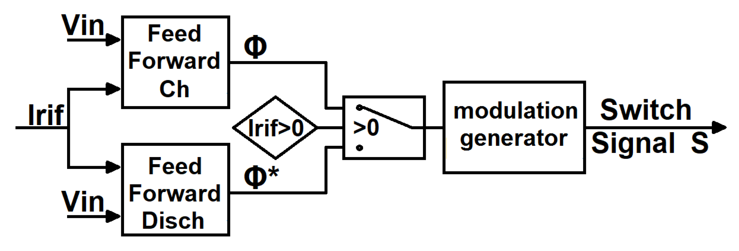
7. Control Algorithm

In order to manage the power flow between the ESS based on the SMHB and DC telecom microgrid, current control of the SMHB was implemented. In particular, in order to allow for a correct comparison between the DC-DC converters under evaluation, a battery current feed-forward control algorithm based on the SMHB model was used, assuming that, by using the same feed-forward control, the performances of modulation techniques could evidence the advantages and disadvantages of the DC-DC converters under investigation. The block scheme used for both the buck–boost and DAB converter is shown in Figure 12.
Regarding the buck–boost converter, the feed-forward algorithm was synthesised, referring to well-known equations linking the power and phase shift regulators. The synthesis of the DAB feed-forward control algorithm has required additional effort. The use of analytic formulation reported in the technical literature has allowed for the definition of the relation between the battery voltage and phase shift of the modulation signal. For this reason, a series of simulations were performed to evaluate the effective relations between the phase shift and voltage to provide the required battery current for the designed DAB.
The simulations, developed in a steady state fixing the phase shift, have allowed for the determination of a lookup table reporting the correspondence between the battery current and phase shift in the case of SPS and TPS during charging and discharging. A curve-fitting procedure was performed to evaluate the function representing the relation between the output battery current and the phase shift. The result of this procedure is reported in (15). The four-order polynomial equation performs a feed-forward control of the phase shift.
D 1 = a 1 I b a t t 4 + a 2 I b a t t 3 + a 3 I b a t t 2 + a 4 I b a t t + a 5
Figure 13 shows the phase shift according to the battery current in the case of the charge phase with TPS and SPS modulation (green curve and cyan curve, respectively) and, similarly, during the discharge phase with TPS and SPS modulation (red curve and violet curve, respectively). The circled curves show the look-up table points obtained by the simulations. The dashed traces report the corresponding relationship considering the analytical formulations reported in technical literature. In Table 5, the parameters identified through the curve-fitting procedure are shown.
Equation (15) connects the phase shift to the current absorbed/supplied by the battery. The effect of parameter variations associated with battery-ageing effects is not significant in SMHBs [39]. Hence, the feed-forward function developed can be considered as intrinsically robust. In the case of SPS modulation, this parameter represents the phase shift between the voltage at the primary and secondary side of the transformer (Figure 9A). In the case of the TPS, this parameter represents the phase shift between the switches S 1 and S 4 concerning the circuit diagram shown in Figure 8. In this second case, two other phase shifts remain to be assessed: D 2 or the phase shift between the switches S 5 and S 6 and D 3 or the phase shift between the voltages at the primary and secondary as shown in Figure 9B. These two parameters can be used to obtain one of the significant advantages of the TPS modulation, which is the cancellation of the flow-back currents, which leads to an improved efficiency [40]. In order to obtain the maximum power transfer, the relation between D 1 , D 2 and D 3 is (16):
D 3 = 1 D 1 D 1 < k k + 1 D 2 = 1 + k ( D 1 1 ) D 1 k k + 1

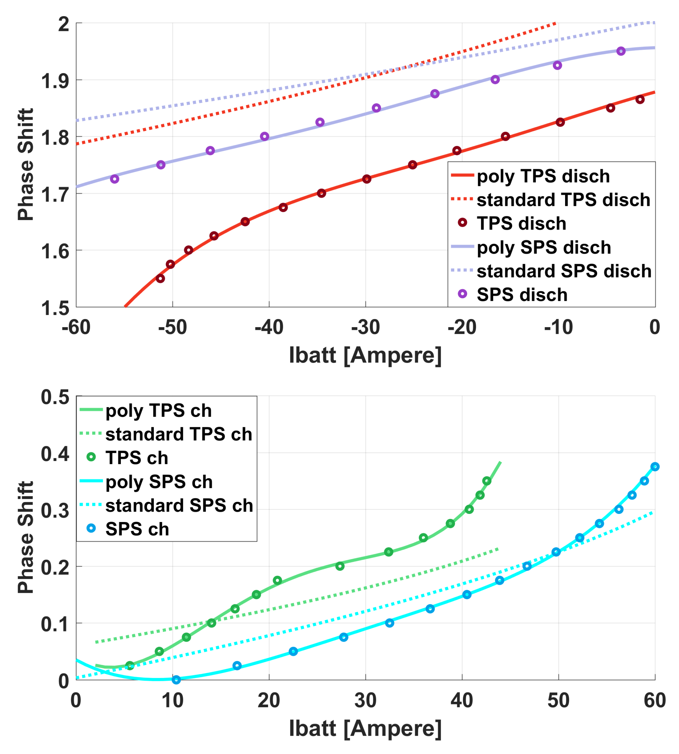
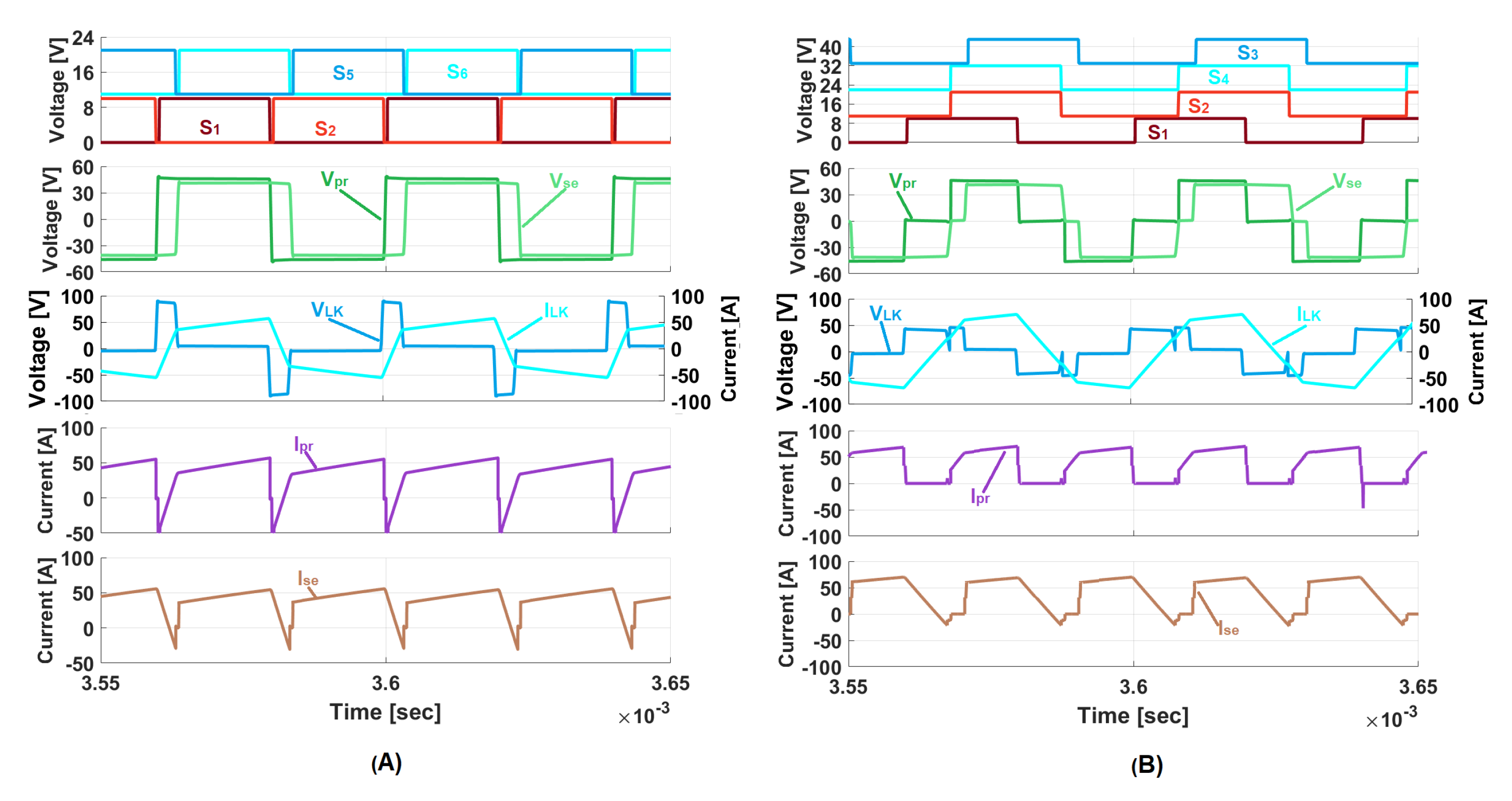
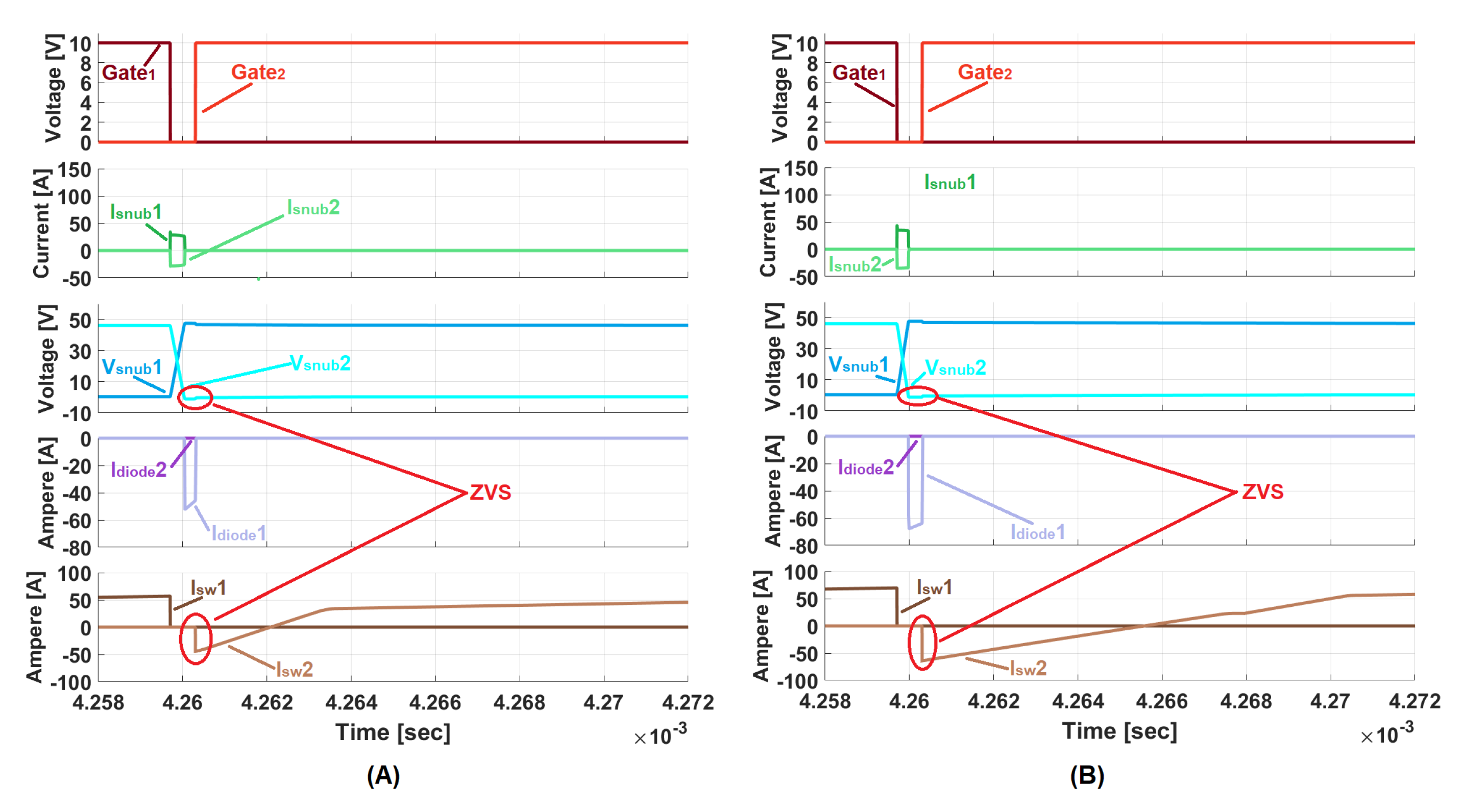
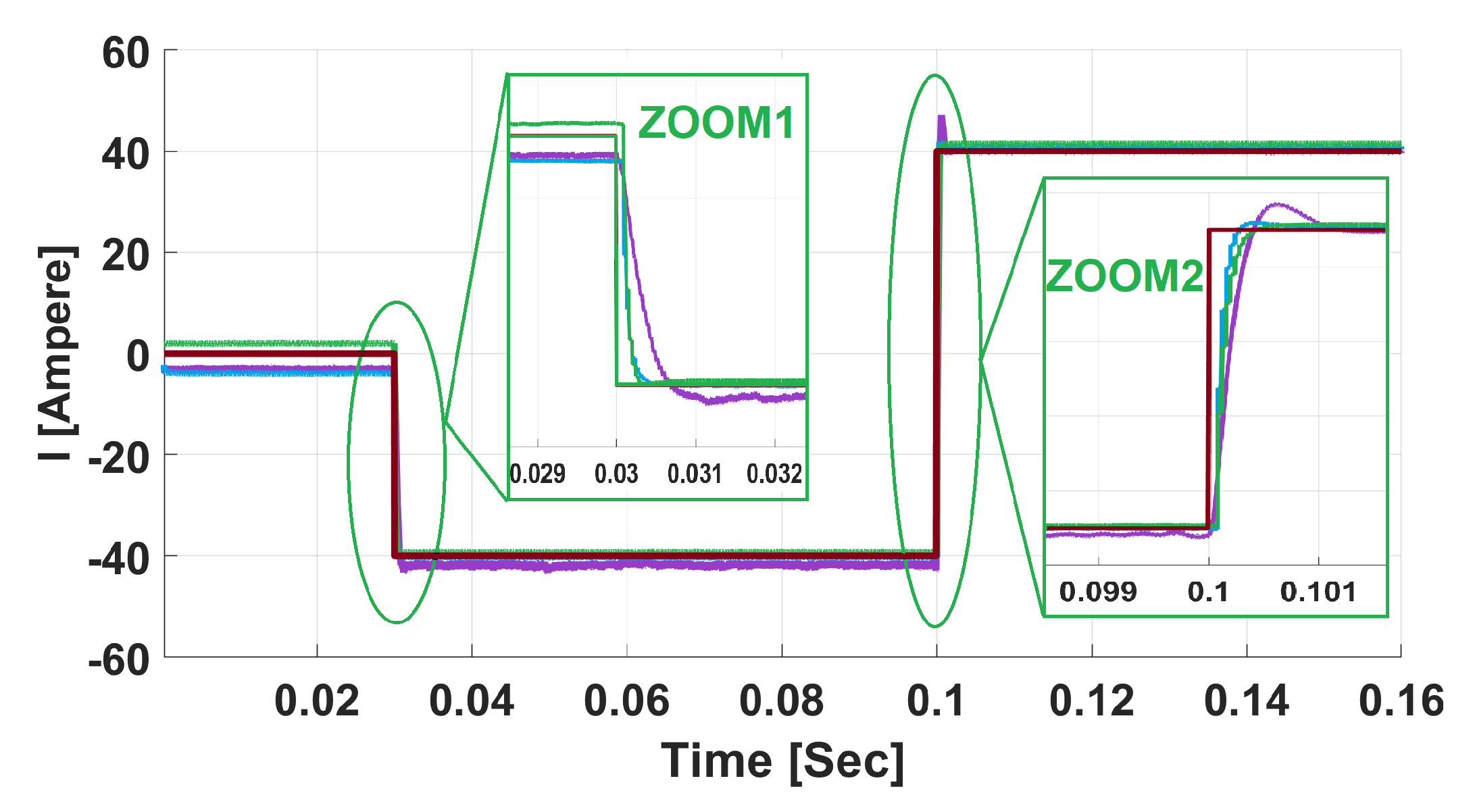
8. Results and Discussion

In order to compare the effects of the proposed design of buck–boost and DAB converters on the performance of SMHB-ESSs used in the DC telecom microgrid, three models were implemented in the Matlab/Simulink environment. For the DAB converter, SPS and the TPS modulation techniques were performed. The control implemented for the energy management of the interface between the ESS and DC microgrid is the feed-forward control technique described in the previous paragraph. The first aspect assessed is the correct operation of the converter. For this purpose, a simulation with a current set-point of 40 A was performed and is reported in Figure 14. It can be observed that the DAB converter operates as expected. The simulation results highlight that the cancellation of the flow-back current on I s e when TPS is implemented cannot be completely achieved, and the same phenomena assume higher values than expected when SPS is implemented.
Furthermore, a simulation analysis was carried out to verify the operation of DAB in ZVS. The simulations were carried out assuming the dynamic phenomena associated to the V-I characteristic and stray capacitance of switches as negligible. Figure 15 shows the simulation results regarding DAB switching when the switch S 1 is opening and S 2 is closing. In particular, when the gate signal on S 1 turns off, the current flows through the two snubber capacities, C s n u b 1 and C s n u b 2 , until their charging and discharging processes end, respectively. Under these voltage conditions, the current passes through the free-wheeling current diode until the dead time is over, and S 2 turns on, allowing for the current to flow. It is important to highlight that the second switch is turned on when the voltage across it is zero, confirming the achievement of ZVS conditions.
The validation of the consistency of the voltage and current performance of DC-DC converters under investigation allows for an analysis of the ESSs when it is interfaced to the DC telecom microgrid. With the aim of assessing the performances under different operating conditions, simulations were developed referring to the DC microgrid demand evolution, which is reported as follows. Specifically, the battery starts in standby conditions ( I r e f = 0 ) with its SoC value equal to 30%. The DC telecom microgrid is characterised by a demand of approximately 2 kW, supplied by the main grid. At t = 0.03 s, an outage of the main network was simulated. The ESS reacts and supplies the DC microgrid, imposing a reference current ( I r e f = 40 A) towards the load. Subsequently, the power grid is restored at ( t = 1 s). The ESS acts so that the battery passes from discharging conditions to a charging one with a reference current of ( I r e f = 40 A). Figure 16 shows the comparison of battery current responses when the proposed DAB, using TPS and SPS, and the buck–boost converters are used as the interface between the SMHB and DC microgrid.
The battery current evolution during discharging and charging properly respond to the current set-point (red curve) for all of the converter topologies proposed, confirming that the feed-forward control based on SMHB modelling provides correct voltage control on the battery for its current management. Furthermore, the response times to the set point variation are very short: equal to 2.5 ms and 5 ms for the DAB and the buck–boost, respectively. Therefore, a more accurate voltage control is expected in the presence of an additional feed-back control algorithm.
Finally, simulations were executed in order to evaluate the conduction and switching losses on diodes and transistors. In order to make the power losses studies comparable, all of the converters were equipped with the same MOSFET and anti-parallel diode. In particular, the model “IPP039N10N5” produced by “Infineon” was used.
In Table 6, the results about the switching and conduction losses are reported. The DAB converter represents the best choice compared to the buck–boost converter. It is also important to highlight that this improvement is due to the zero switching losses since this converter operates in ZVS conditions. In Table 7, the features of the DC-DC converter under analysis are reported for a complete performance comparison.
The difference between the SPS and the TPS is not very high in terms of converter losses.Therefore, in order to evaluate which modulation represents the optimal choice for this application, it may be useful to consider another important aspect, such as the current stress. In this case, the peak of the current on the inductor in the two cases is practically equal (Figure 14), but, considering the TPS, the waveforms show slower dynamic variations in the inductor current than those obtained from the SPS, leading to a reduction in the current stress on the transformer.

9. Conclusions

This paper uses an integrated method for modelling, controlling and designing Energy Storage Systems (ESSs) based on Sodium Metal Halide Batteries (SMHBs) characterised by a rated voltage lower than that of the supported telecom DC microgrid that has been proposed and verified through simulation tests. Specifically, the proposed design procedure was applied to two different DC-DC converters topologies. The considered topologies are the buck–boost converter and the DAB converter. In order to assess the advantages that are obtainable by using advanced modelling in energy storage system based on sodium metal halide technology, a performance analysis was developed considering a reduced number of cells per battery string such that the rated battery voltage assumes a value of 39 V. The performances were evaluated considering a simple feed-forward control scheme for the buck–boost and DAB converter. Two modulation techniques, SPS and TPS, were adopted for the DAB converter. Simulation results demonstrate the feasibility of downsizing the number of string cells of the SMHB, extending the operative state of charge by implementing a battery management system based on advanced battery modelling. In particular, the proper operation of the converters, which manage the power flows between the SMHB and the 48 V DC telecommunications grid, allows for the achievement of required performances in all of the possible operating conditions. Higher dynamic performances (with short response times (5 ms)) are verified in the case of the DAB converter. Better performances are registered also in terms of converter losses in the case of the DAB when the TPS is employed. This suggests that the DAB converter is a suitable candidate for DC telecom microgrids supported by sodium metal halide batteries.

Author Contributions

Conceptualization, M.B., A.F. and A.D.; methodology, A.D., M.B. and R.A.M.; software, M.B. and A.F.; validation, A.D., M.B. and R.A.M.; formal analysis, M.B., A.F. and A.D.; investigation, M.B. and A.F.; data curation, M.B. and A.F.; writing—A.F., M.B. and A.D.; writing—review and editing, A.F., M.B. and A.D.; visualization, A.F., M.B. and A.D.; supervision, A.D. All authors have read and agreed to the published version of the manuscript.

Funding

This research received no external funding.

Data Availability Statement

Data is contained within the article.

Conflicts of Interest

The authors declare no conflict of interest.

References

  1. Damiano, A.; Musio, C.; Marongiu, I. Experimental validation of a dynamic energy model of a battery electric vehicle. In Proceedings of the 2015 International Conference on Renewable Energy Research and Applications (ICRERA), Palermo, Italy, 22–25 November 2015; pp. 803–808. [Google Scholar] [CrossRef]
  2. D‘Agostino, R.; Baumann, L.; Damiano, A.; Boggasch, E. A Vanadium-Redox-Flow-Battery Model for Evaluation of Distributed Storage Implementation in Residential Energy Systems. IEEE Trans. Energy Convers. 2015, 30, 421–430. [Google Scholar] [CrossRef]
  3. Di Rienzo, R.; Simonte, G.; Biagioni, I.; Baronti, F.; Roncella, R.; Saletti, R. Experimental Investigation of an Electrical Model for Sodium–Nickel Chloride Batteries. Energies 2020, 13, 2652. [Google Scholar] [CrossRef]
  4. Sun, X.; Li, Z.; Wang, X.; Li, C. Technology Development of Electric Vehicles: A Review. Energies 2019, 13, 90. [Google Scholar] [CrossRef] [Green Version]
  5. Young, K. Research in Nickel/Metal Hydride Batteries 2017. Batteries 2018, 4, 9. [Google Scholar] [CrossRef] [Green Version]
  6. Restello, S.; Lodi, G.; Miraldi, A.K. Sodium Nickel Chloride Batteries for telecom application: A solution to critical high energy density deployment in telecom facilities. In Proceedings of the Intelec 2012, Scottsdale, AZ, USA, 30 September–4 October 2012; pp. 1–6. [Google Scholar] [CrossRef]
  7. Benato, R.; Cosciani, N.; Crugnola, G.; Sessa, S.D.; Lodi, G.; Parmeggiani, C.; Todeschini, M. Sodium nickel chloride battery technology for large-scale stationary storage in the high voltage network. J. Power Sources 2015, 293, 127–136. [Google Scholar] [CrossRef]
  8. Boi, M.; Battaglia, D.; Salimbeni, A.; Damiano, A. A Novel Electrical Model for Iron Doped-Sodium Metal Halide Batteries. IEEE Trans. Ind. Appl. 2019, 55, 6247–6255. [Google Scholar] [CrossRef]
  9. Boi, M.; Battaglia, D.; Salimbeni, A.; Damiano, A. A non-linear electrical model for iron-doped sodium metal halides batteries. In Proceedings of the 10th IEEE Energy Conversion Congress & Expo ECCE, Portland, OR, USA, 23–27 September 2018; pp. 2039–2046. [Google Scholar]
  10. Qi, Q.; Ghaderi, D.; Guerrero, J.M. Sliding mode controller-based switched-capacitor-based high DC gain and low voltage stress DC-DC boost converter for photovoltaic applications. Int. J. Electr. Power Energy Syst. 2021, 125, 106496. [Google Scholar] [CrossRef]
  11. Ertekin, D.; Bulut, K.; Tekin, H.; Moschopoulos, G. A design for switched capacitor and single-switch DC–DC boost converter by a small signal-based PI controller. Int. J. Circuit Theory Appl. 2022, 50, 1620–1651. [Google Scholar] [CrossRef]
  12. Magar, A.V.; Kanade, S.G.; Kinge, A.P. Transformerless Buck-Boost DC-DC Converter. In Proceedings of the 2018 IEEE Global Conference on Wireless Computing and Networking (GCWCN), Lonavala, India, 23–24 November 2018; pp. 200–203. [Google Scholar]
  13. Barone, G.; Brusco, G.; Burgio, A.; Motta, M.; Menniti, D.; Pinnarelli, A.; Sorrentino, N. A dual active bridge dc-dc converter for application in a smart user network. In Proceedings of the 2014 Australasian Universities Power Engineering Conference (AUPEC), Perth, Australia, 28 September–1 October 2014; pp. 1–5. [Google Scholar] [CrossRef]
  14. Vieira, A.; Mazza, L.; Antunes, F.; Oliveira, D. Bidirectional dual-active-bridge DC-DC converter for vehicle-to-grid applications in DC microgrids. In Proceedings of the 2018 Simposio Brasileiro de Sistemas Eletricos (SBSE), Niteroi, Brazil, 12–16 May 2018; pp. 1–6. [Google Scholar] [CrossRef]
  15. Gorji, S.A.; Sahebi, H.G.; Ektesabi, M.; Rad, A.B. Topologies and Control Schemes of Bidirectional DC–DC Power Converters: An Overview. IEEE Access 2019, 7, 117997–118019. [Google Scholar] [CrossRef]
  16. ETSI EN 300 132-1 V2.0.1 (2017-11); Environmental Engineering (EE); Power Supply Interface at the Input to Information and Communication. ETSI: Valbonne, France, 2017.
  17. ETSI EN 300 132-2 V2.5.1 (2016-10); Environmental Engineering (EE); Power Supply Interface at the Input to Telecommunications and Datacom (ICT) Equipment; Part 2: Operated by -48 V Direct Current (dc). ETSI: Valbonne, France, 2016.
  18. ETSI EN 300 132-3 V2.1.1 (2011-10); Environmental Engineering (EE); Power Supply Interface at the Input to Telecommunications and Datacom (ICT) Equipment; Part 3: Operated by Rectified Current Source, Alternating Current Source or Direct Current Source up to 400 V. ETSI: Valbonne, France, 2011.
  19. Deevela, N.R.; Singh, B.; Kandpal, T.C. Load Profile of Telecom Towers and Potential Renewable Energy Power Supply Configurations. In Proceedings of the 2018 IEEE International Conference on Power Electronics, Drives and Energy Systems (PEDES), Chennai, India, 18–21 December 2018; pp. 1–6. [Google Scholar] [CrossRef]
  20. Olatomiwa, L.J.; Mekhilef, S.; Huda, A.S.N. Optimal sizing of hybrid energy system for a remote telecom tower: A case study in Nigeria. In Proceedings of the 2014 IEEE Conference on Energy Conversion (CENCON), Johor Bahru, Malaysia, 13–14 October 2014; pp. 243–247. [Google Scholar] [CrossRef]
  21. Mangu, B.; Kumar, K.K.; Fernandes, B.G. A novel grid interactive hybrid power supply system for telecom application. In Proceedings of the 2011 Annual IEEE India Conference, Hyderabad, India, 16–18 December 2011; pp. 1–5. [Google Scholar] [CrossRef]
  22. Eaves, S.S.; Mlyniec, S. Lithium-ion batteries in telecom Hybrid Power Systems. In Proceedings of the 2011 IEEE 33rd International Telecommunications Energy Conference (INTELEC), Amsterdam, The Netherlands, 9–13 October 2011; pp. 1–3. [Google Scholar] [CrossRef]
  23. O’Sullivan, T.M.; Bingham, C.M.; Clark, R.E. Zebra battery technologies for all electric smart car. In Proceedings of the International Symposium on Power Electronics, Electrical Drives, Automation and Motion (SPEEDAM 2006), Capri, Italy, 22–24 June 2006; p. 243. [Google Scholar] [CrossRef] [Green Version]
  24. Zhang, J.; Lai, J.; Kim, R.; Yu, W. High-Power Density Design of a Soft-Switching High-Power Bidirectional dc ndash;dc Converter. IEEE Trans. Power Electron. 2007, 22, 1145–1153. [Google Scholar] [CrossRef]
  25. Jain, A.K.; Ayyanar, R. Pwm control of dual active bridge: Comprehensive analysis and experimental verification. IEEE Trans. Power Electron. 2011, 26, 1215–1227. [Google Scholar] [CrossRef]
  26. Ahmed Adam, A.H.; Hou, S.; Chen, J. ZVS Operation Range Analysis and Deadband Conditions of A dual H-bridge Bidirectional DC-DC Converter with Phase Shift Control. In Proceedings of the 2019 IEEE International Conference on Environment and Electrical Engineering and 2019 IEEE Industrial and Commercial Power Systems Europe (EEEIC/I CPS Europe), Genova, Italy, 11–14 June 2019; pp. 1–6. [Google Scholar]
  27. Higa, H.; Itoh, J. Zero voltage switching over entire load range and wide voltage variation of parallelly-connected dual-active-bridge converter using power-circulating operation. In Proceedings of the 2017 IEEE 3rd International Future Energy Electronics Conference and ECCE Asia (IFEEC 2017-ECCE Asia), Kaohsiung, Taiwan, 3–7 June 2017; pp. 506–511. [Google Scholar]
  28. Zhao, B.; Yu, Q.; Sun, W. Extended-Phase-Shift Control of Isolated Bidirectional DC–DC Converter for Power Distribution in Microgrid. IEEE Trans. Power Electron. 2012, 27, 4667–4680. [Google Scholar] [CrossRef]
  29. Wen, H.; Su, B.; Xiao, W. Design and performance evaluation of a bidirectional isolated dc-dc converter with extended dual-phaseshift scheme. IET Power Electron. 2013, 6, 914–924. [Google Scholar] [CrossRef]
  30. Zhao, B.; Song, Q.; Liu, W. Power Characterization of Isolated Bidirectional Dual-Active-Bridge DC–DC Converter With Dual-Phase-Shift Control. IEEE Trans. Power Electron. 2012, 27, 4172–4176. [Google Scholar] [CrossRef]
  31. Harrye, Y.A.; Ahmed, K.H.; Adam, G.P.; Aboushady, A.A. Comprehensive steady state analysis of bidirectional dual active bridge DC/DC converter using triple phase shift control. In Proceedings of the 2014 IEEE 23rd International Symposium on Industrial Electronics (ISIE), Istanbul, Turkey, 1–4 June 2014; pp. 437–442. [Google Scholar]
  32. Bu, Q.; Wen, H. Triple-Phase-Shifted Bidirectional Full-Bridge Converter with Wide range ZVS. In Proceedings of the 2018 IEEE International Conference on Power Electronics, Drives and Energy Systems (PEDES), Chennai, India, 18–21 December 2018; pp. 1–6. [Google Scholar]
  33. Rodríguez, A.; Vázquez, A.; Lamar, D.G.; Hernando, M.M.; Sebastián, J. Different Purpose Design Strategies and Techniques to Improve the Performance of a Dual Active Bridge With Phase-Shift Control. IEEE Trans. Power Electron. 2015, 30, 790–804. [Google Scholar] [CrossRef]
  34. Yazdani, F.; Zolghadri, M. Design of dual active bridge isolated bi-directional DC converter based on current stress optimization. In Proceedings of the 8th Power Electronics, Drive Systems & Technologies Conference (PEDSTC), Mashhad, Iran, 14–16 February 2017; pp. 247–252. [Google Scholar] [CrossRef]
  35. Rodríguez Alonso, A.R.; Sebastian, J.; Lamar, D.G.; Hernando, M.M.; Vazquez, A. An overall study of a Dual Active Bridge for bidirectional DC/DC conversion. In Proceedings of the 2010 IEEE Energy Conversion Congress and Exposition, Atlanta, GA, USA, 12–16 September 2010; pp. 1129–1135. [Google Scholar]
  36. Zhao, B.; Song, Q.; Liu, W.; Sun, Y. A Synthetic Discrete Design Methodology of High-Frequency Isolated Bidirectional DC/DC Converter for Grid-Connected Battery Energy Storage System Using Advanced Components. IEEE Trans. Ind. Electron. 2014, 61, 5402–5410. [Google Scholar] [CrossRef]
  37. Garcia-Bediaga, A.; Villar, I.; Rujas, A.; Mir, L.; Rufer, A. Multiobjective Optimization of Medium-Frequency Transformers for Isolated Soft-Switching Converters Using a Genetic Algorithm. IEEE Trans. Power Electron. 2017, 32, 2995–3006. [Google Scholar] [CrossRef]
  38. Ruiz-Robles, D.; Venegas-Rebollar, V.; Anaya-Ruiz, A.; Moreno-Goytia, E.; Rodríguez-Rodríguez, J. Design and Prototyping Medium-Frequency Transformers Featuring a Nanocrystalline Core for DC–DC Converters. Energies 2018, 11, 2081. [Google Scholar] [CrossRef] [Green Version]
  39. Benato, R.; Dambone Sessa, S.; Musio, M.; Palone, F.; Polito, R.M. Italian Experience on Electrical Storage Ageing for Primary Frequency Regulation. Energies 2018, 11, 2087. [Google Scholar] [CrossRef] [Green Version]
  40. Wu, F.; Feng, F.; Gooi, H.B. Cooperative Triple-Phase-Shift Control for Isolated DAB DC–DC Converter to Improve Current Characteristics. IEEE Trans. Ind. Electron. 2019, 66, 7022–7031. [Google Scholar] [CrossRef]
Figure 1. General identification of the interfaces in ETSI EN 300 132 standard.
Energies 16 02169 g001
Figure 2. Schematic representation of sodium metal halide cell.
Energies 16 02169 g002
Figure 3. A schematic description of the SMHC during the discharge phase.
Energies 16 02169 g003
Figure 4. Advanced electrical model of SMHB including iron-doping effects.
Energies 16 02169 g004
Figure 5. Topology of single-phase bidirectional buck–boost converter.
Energies 16 02169 g005
Figure 6. Inductor current during buck mode. I p e a k with V g r i d = 50 V (green curve), I p e a k with V g r i d = 40 V (blue curve), I m i n with V g r i d = 50 V (red curve) and I m i n with V g r i d = 40 V (cyan curve).
Energies 16 02169 g006
Figure 7. Inductor current during boost mode. I p e a k with V g r i d = 57 V (green curve), I p e a k with V g r i d = 50 V (blue curve), I m i n with V g r i d = 50 V (cyan curve) and I m i n with V g r i d = 57 V (red curve).
Energies 16 02169 g007
Figure 8. Topology of bidirectional dual-active-bridge converter.
Energies 16 02169 g008
Figure 9. Standard waveforms for SPS (A) and TPS (B) modulations.
Energies 16 02169 g009
Figure 10. Operating regions in ZVS conditions.
Energies 16 02169 g010
Figure 11. Analysis of DAB converter ZVS range at rated power for the case study.
Energies 16 02169 g011
Figure 12. Converters control scheme.
Energies 16 02169 g012
Figure 13. Phase shift with respect to current set-point using polynomial function (full lines) and standard equations (doted lines) during both charge and discharge phase.
Energies 16 02169 g013
Figure 14. Simulated waveforms obtained imposing a charging current set-point of 40 A to the model shown in Figure 8 using the algorithm SPS (A) and (TPS) (B).
Energies 16 02169 g014
Figure 15. Switching phase of first leg in ZVS conditions when the switch S 1 is opening and S 2 is closing using the algorithm SPS (A) and (TPS) (B).
Energies 16 02169 g015
Figure 16. Battery current evolution during charge phase for DAB with TPS (blue curve), DAB with SPS (green curve) and buck–boost converter (violet curve). Red curve represents the current set-point.
Energies 16 02169 g016
Table 1. Normal and abnormal service voltage interval at the interface “ A x ” according to the standard “ETSI EN 300 132:part 2”.
Admissible voltage range in normal operationPerformance criteria
From 40.5 V to 57.0 VNo degradation in the service performance during and after the test
Admissible voltage range in abnormal operation
From 40.5 V to 60.0 VSelf-restart to a normal service of the equipment without operator intervention
Table 2. Buck–boost converter parameters of proposed SMHB-based ESS.
ParameterValueUnit
C h i g h 1.75mF
C l o w 1.75mF
L13.1 μ H
Switch Parameters
MOSFET on resistance6m Ω
Diode on resistance3.7m Ω
MOSFET off conductance11/ μ Ω
Diode off conductance101/ μ Ω
Table 3. DAB converter parameters.
ParameterSymbolValueUnit
Switching Frequency f s w 25kHz
Death Time t m 600nsec
Leakage Inductance L k 3.42 μ H
Snubber Capacitance C s n u b 200nF
Grid Side Parameters
Grid Voltage V g r i d 50V
Grid Resistance R g r i d 0.1 Ω
Grid Capacitance C 1 17.5mF
Battery Side Parameters
Battery Voltage V o c 39V
Battery Internal Resistance R b a t t 0.04 Ω
Battery Capacitance C 2 17.5mF
Switch Parameters
MOSFET on resistance R o n 6m Ω
Diode on resistance R o n 3.7m Ω
MOSFET off conductance C o f f 11/ μ Ω
Diode off conductance C o f f 101/ μ Ω
Table 4. Equivalent circuit DAB transformer parameters.
ParameterSymbolValueUnit
Output Power A D A B 2000VA
Operating Frequency f n 25kHz
Linkage Inductance L M 270 μ H
Core Losses Equivalent Resistance R M 1000 Ω
Leakage Inductance L k 3.4 μ H
Copper Losses Equivalent Resistance R 0 5.8m Ω
Table 5. Curve-fitting parameters for polynomial function in feed-forward control.
ParametersTPS ChTPS DischSPS ChSPS Disch
a1 8.449 × 10 7 6.909 × 10 8 1.41 × 10 7 4.263 × 10 8
a2 7.264 × 10 5 4.84 × 10 6 1.671 × 10 5 6.159 × 10 6
a3 2.007 × 10 3 9.843 × 10 5 7.448 × 10 4 3.008 × 10 4
a4 1.188 × 10 2 4.622 × 10 3 9.286 × 10 3 1.215 × 10 3
a50.041951.8780.035111.944
Table 6. Buck–boost and DAB converters conduction and switching losses at different current set-points.
Current Set-PointBuck–BoostSPSTPS
40 A53.34 W48 W48 W
20 A48.57 W17.6 W14.24 W
−20 A53.47 W16 W14.64 W
−40 A81.53 W48.16 W45.52 W
Table 7. DC-DC converters feature comparison.
TopologyNumber Sw-L-C-DV GainVoltage StressZVSEfficiency
Classic Buck–Boost1-1-1-1 D 1 D V i n + V 0 yes97.3%
DAB8-1-1-8 R L n f s w L k ϕ ( 1 2 ϕ ) V b u s yes98%
Disclaimer/Publisher’s Note: The statements, opinions and data contained in all publications are solely those of the individual author(s) and contributor(s) and not of MDPI and/or the editor(s). MDPI and/or the editor(s) disclaim responsibility for any injury to people or property resulting from any ideas, methods, instructions or products referred to in the content.

