Article

A High-Efficiency QR Flyback DC–DC Converter with Reduced Switch Voltage Stress Realized by Applying a Self-Driven Active Snubber (SDAS)

1
Department of Electronics Engineering, Cheongju University, Cheongju 28503, Republic of Korea
2
R&D Division, Zinnos Inc., Busan 49108, Republic of Korea
3
Department of Electrical & Control Engineering, Cheongju University, Cheongju 28503, Republic of Korea
*
Author to whom correspondence should be addressed.
Energies 2023, 16(3), 1068; https://doi.org/10.3390/en16031068
Submission received: 21 December 2022 / Revised: 12 January 2023 / Accepted: 13 January 2023 / Published: 18 January 2023
(This article belongs to the Topic Power Converters)

Abstract

:
In this paper, a QR flyback converter using a self-driven active snubber (SDAS) was proposed to solve the problem of voltage surge in the switch of QR flyback converters. In the proposed converter, the SDAS consisting of a clamping capacitor and an active switch can be configured in parallel with the main switch or transformer to reduce the voltage surge in the switch. To confirm the steady-state characteristics of the QR flyback converter to which the proposed SDAS is applied, equivalent circuits for each state were constructed, and the equations and characteristics for each state were determined. A 60 W class small AC–DC adapter was constructed to confirm the effectiveness of the proposed converter and the control circuit method, and the experimental results were analyzed. The size of the experimental AC–DC adapter was 74 × 29 × 23   mm , and it had a high power density of 20   W / in 3 or more. The experimental circuit was limited to the high power conversion efficiency of up to 91.56%, and the maximum voltage surge in the switch was approximately 450 V. One of the reasons for such high efficiency is the SDAS circuit, which sufficiently reduces the voltage surge of the QR flyback switch, compared with the RCD clamp circuit, and does not consume power in principle.

1. Introduction

Recently, due to the rapid development of the IT field, low-power energy consumption and high-efficiency power conversion devices are required. Following the trend of miniaturization and lightweight electronic devices, research is being actively conducted to increase the efficiency of power converters and reduce their weight. To reduce the size and weight of power supply devices, high-frequency switching has become an important design criterion. A switching power supply is a device that converts an input voltage into a stable output voltage, and appropriate circuit development is required depending on the application field and output capacity. For output powers of less than 150 W, flyback converters are most commonly used to achieve miniaturization and low manufacturing cost. In addition, since a transformer is used, multiple outputs can be comprised, and input and output isolation is possible [1,2].
Recently, with the introduction of the quasi-resonant (QR) flyback control method, the switching loss is reduced, and efficiency is increased compared with conventional flyback converters, resulting in a broader range of applications. The power conversion efficiency can be increased by reducing the turn-on loss to reduce the switching loss. However, in the case of an isolated switching power supply such as a QR flyback converter, a turn-off surge in voltage simultaneously occurs across the switch due to internal parasitic components. This high-voltage surge increases the rated voltage of the switch and becomes a major cause of deterioration in the reliability of the product. To reduce high-voltage switch surges, an RCD-structured snubber using a resistor–capacitor–diode can be used across the primary and secondary sides of the transformer or the switch. The RCD snubber has the advantage of having a simple structure and easy design, but it also generates heat in the resistance element and lowers the power conversion efficiency of the converter because the entire energy resulting from the high surge in voltage is consumed in the resistor.
Another way to reduce the voltage surge in the switch is to apply an active clamp circuit by configuring the auxiliary switch in series with the clamp capacitor separately from the main switch. In this case, one of the methods to clamp the main switch voltage to a constant voltage is by introducing a signal in the drive signal of the main switch that is opposite to that of the auxiliary switch. However, this active clamp method cannot be applied to all flyback converter methods and only applies to converters operating in the boundary current mode (BCM), in which the transformer magnetizing inductor current is at the boundary at zero but not applicable to the quasi-resonant (QR) flyback method, which operates in discontinuous conduction mode (DCM) [3,4].
Figure 1 shows the basic circuit of a QR flyback converter with an RCD snubber. Figure 1a shows a converter in which the secondary side of the transformer is composed of a diode rectifier, while Figure 1b shows a converter composed of a synchronous rectifier circuit using MOSFET instead of a diode. In Figure 1a, the main switch of the converter is S , and the resistance R s , capacitor C s , and diode D s of the RCD snubber are in parallel with the transformer T 1 , and the surge energy due to the resonance of the transformer leakage inductor L K and the switch parasitic capacitor C R is consumed in the RCD snubber circuit. In Figure 1b, the main switch of the converter is S 1 , and the synchronous rectifier switch S R replaces the diode rectifier on the secondary side of the transformer T 1 . Figure 2 shows the operating waveform in a steady state. Figure 2a is the voltage and current waveform of the diode rectifier, and Figure 2a is the driving signal and the voltage and current waveform of the MOSFET synchronous rectifier. In the QR flyback converter, the magnetizing current of the transformer increases linearly from zero during the turn-on period of the switch because it operates at the DCM and the continuous conduction mode (CCM). During the turn-off period, a voltage surge is generated during damping resonance due to the transformer leakage inductor and the parasitic capacitor of the switch. Although the RCD snubber circuit absorbs some of the surge current, the remaining current still generates a voltage surge in the switch. At this time, the voltage surge of the switch reaches maximum point, and the voltage surge can cause breakdown of the switch [5]. The secondary-side rectifier current linearly decreases, and after it becomes zero, the resonance resulting from magnetizing inductance L M and the switch parasitic capacitor C R starts, and the main switch is turned on at the valley, where the switch resonance voltage is lowest owing to the QR flyback control signal. In the case of the synchronous rectifier, the synchronous rectifier switch S R is turned on while the rectifier current flows. For the synchronous rectifier switch S R , a MOSFET with low on-resistance is selected to reduce the conduction loss. As shown in Figure 2, since the main switch voltage of the QR flyback converter is turned on when it reaches the lowest point due to resonance, the turn-on loss is reduced, thus reducing switching loss and enabling high-efficiency power conversion. However, since a voltage surge is generated when the switch S is turned off, this problem cannot be fundamentally solved by adding an RCD snubber circuit [6,7,8].
In this paper, a QR flyback converter using a self-driven active snubber (SDAS) is proposed to mitigate the problem of the high switch-turn-off voltage in the QR flyback converter. The proposed converter clamps the voltage surge of the switch to a constant voltage during turn-off operation owing to the SDAS composed of a clamping capacitor and an active switch, and since the active switch drive signal is controlled by the secondary-side current of the transformer, a separate control circuit is not required. In addition, the proposed converter has the advantage of using a switch with a low voltage rating due to the reduced turn-off voltage surge and using the conventional QR flyback control IC. For the design of its major components, the steady-state operation characteristics were analyzed, and the simulation and experimental results were compared. To confirm the effectiveness of the proposed converter and the control circuit method, a 60 W class miniaturized AC–DC adapter was constructed, and the experimental results were analyzed. The size of the experimental AC–DC adapter was 74 × 29 × 23   mm , the power density was about 20   W / in 3 , and the target maximum efficiency was over 90% [9,10,11].

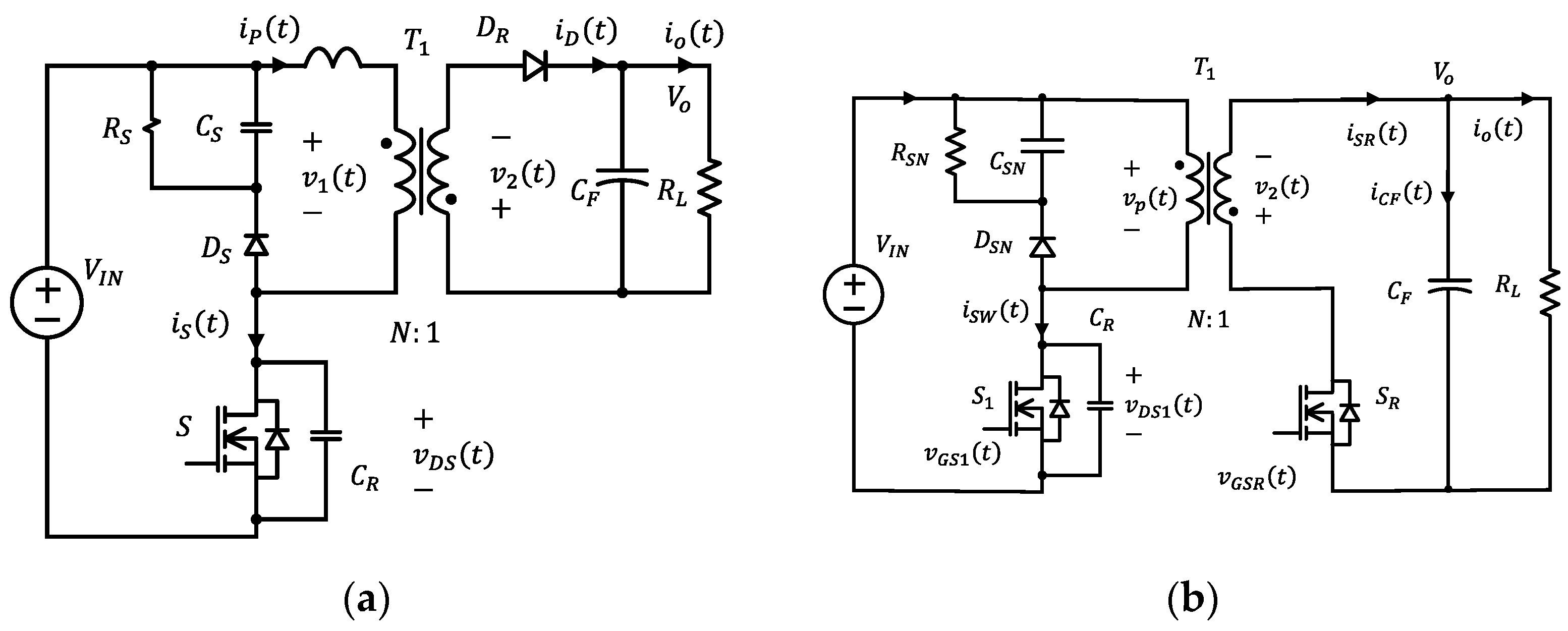
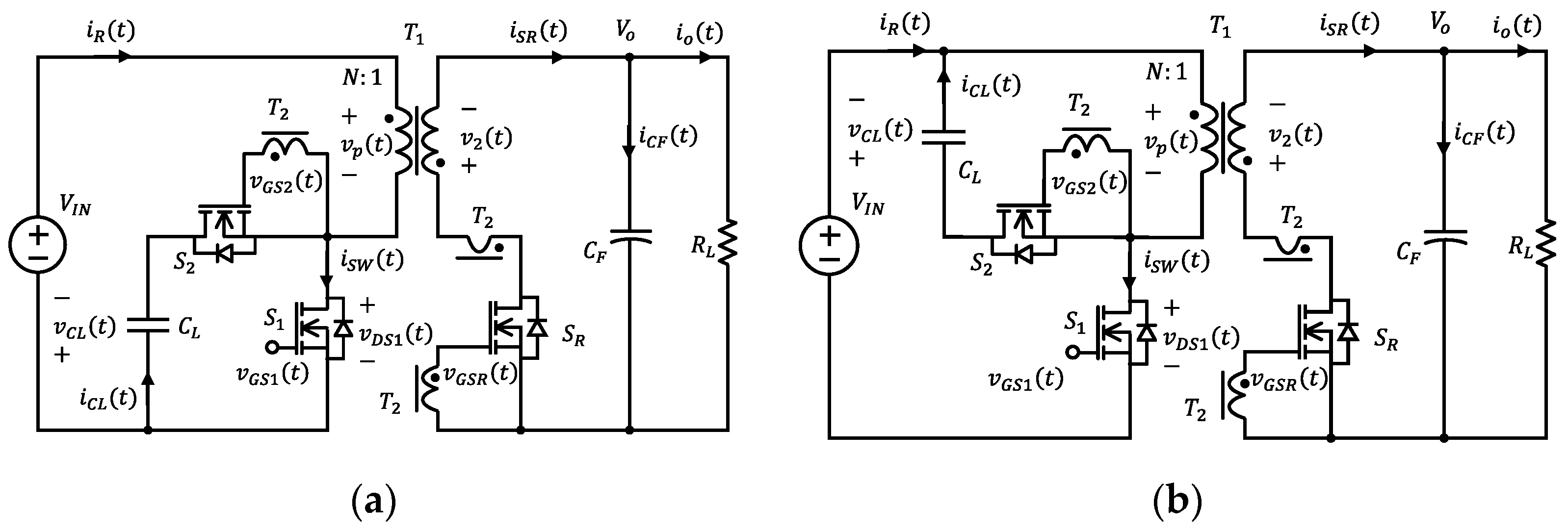
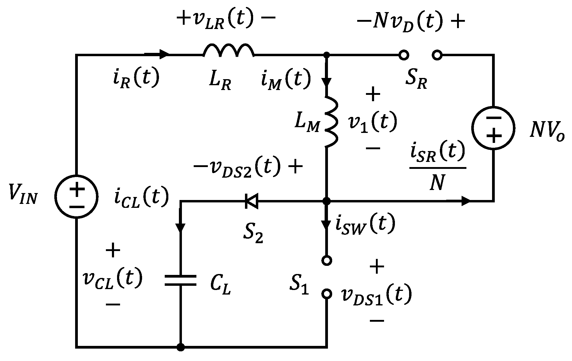
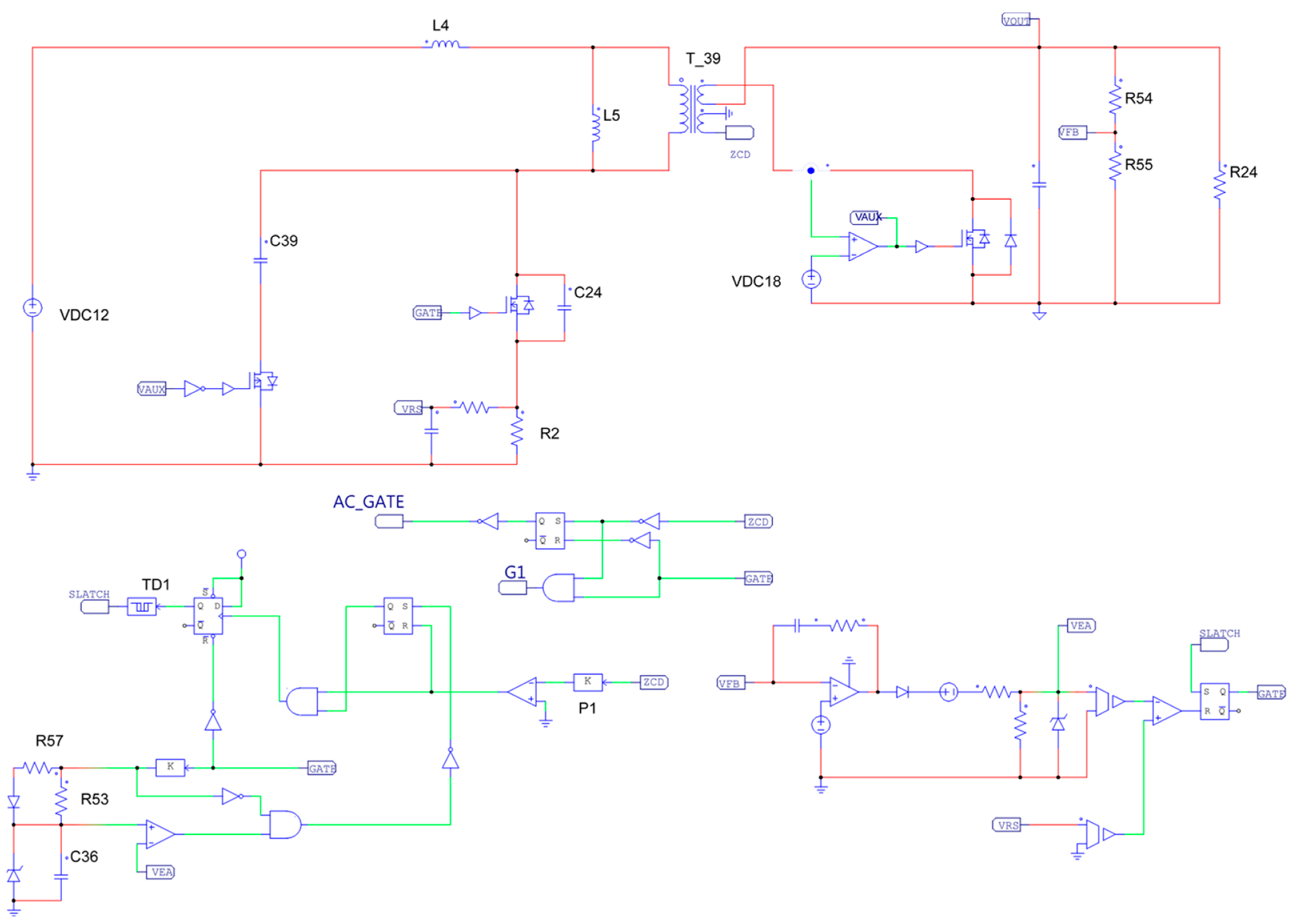
2. QR Flyback DC–DC Converter with SDAS

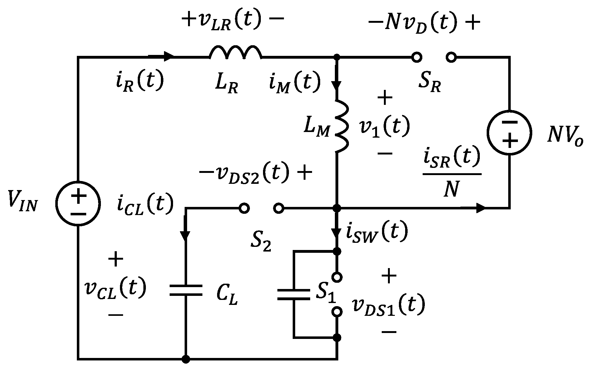
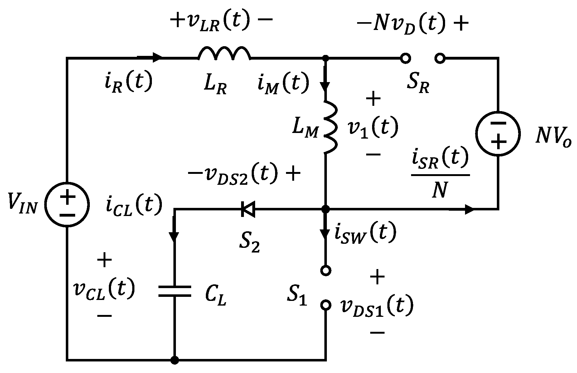
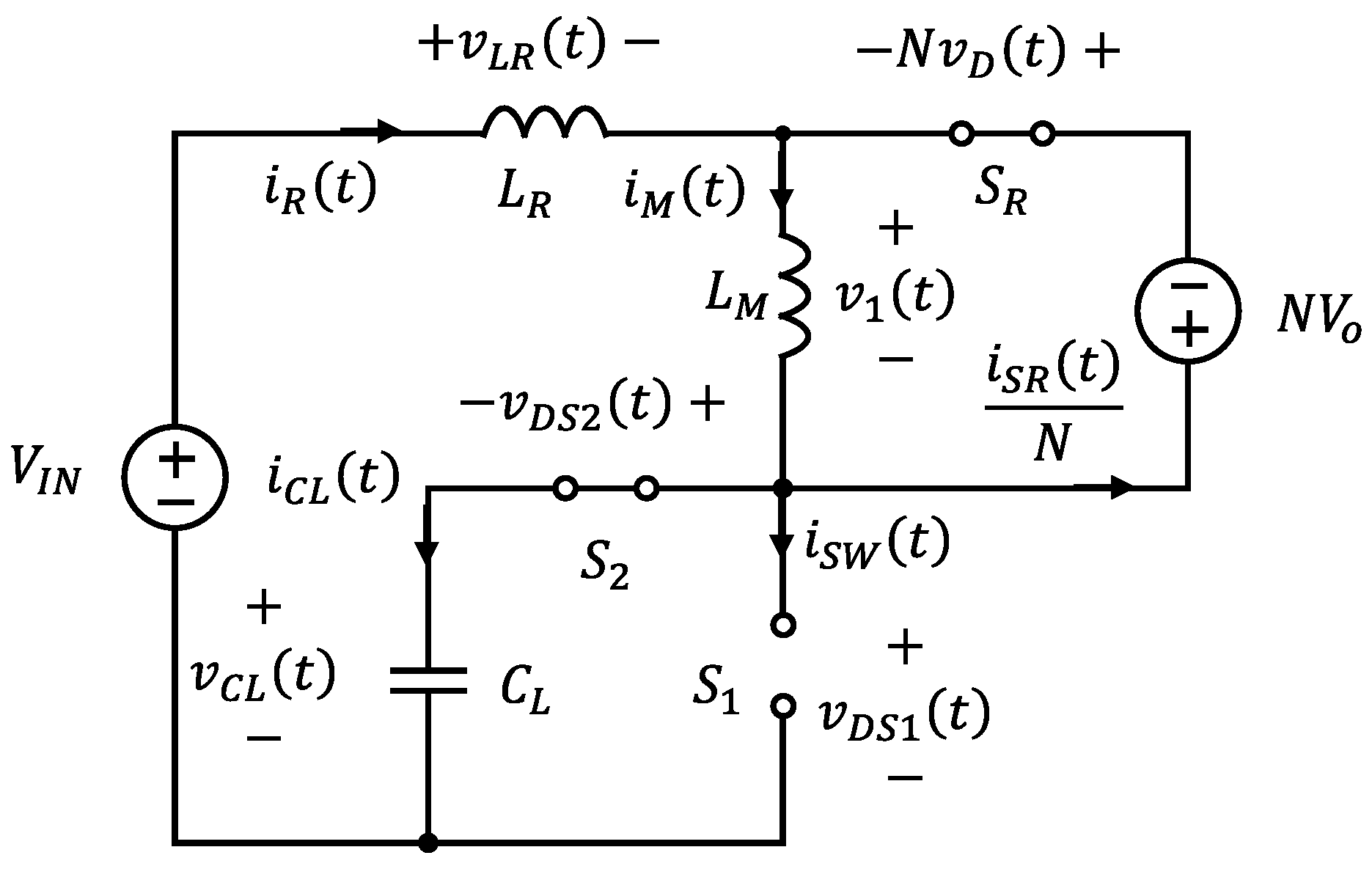
2.1. Basic Circuit Structure of QR Flyback Converter with SDAS

Figure 3 shows the basic circuit of the QR flyback converter with the SDAS proposed in this paper. In Figure 3a, the SDAS is configured in parallel with the main switch, while in Figure 3b, the SDAS is configured in parallel with the transformer. In this figure, the main switch is S 1 , and the synchronous rectifier switch S R replaces the existing diode rectifier on the secondary side of the transformer T 1 . The SDAS circuit consists of a clamp switch S 2 and a clamp capacitor C L in series. Transformer T 2 is a current transformer (CT) that detects secondary-side current and generates driving signals for the synchronous rectifier switch S R and the clamp switch S 2 . Therefore, since the two switches S R and S 2 are turned on and off by the secondary-side current signal of the transformer, they are driven independently of the external PWM control signal. The clamp capacitor C L absorbs the surge energy caused by the resonance of the transformer leakage inductor L K and the switch parasitic capacitor C R . In the conventional active clamp-type flyback converter, the location of the main switch S 1 , the clamp switch S 2 , and the clamp capacitor C L are the same as the circuit proposed in this paper, but the clamp switch S 2 serves as a complementary switch to the main switch, so the QR flyback characteristics are not satisfied. Therefore, the conventional active-clamp flyback converter has different steady-state operation characteristics from the QR flyback converter configured with the SDAS in parallel. Since QR flyback converters are relatively widely applied in the design and manufacturing of small-capacity converters, several manufacturers have released control IC models. In this paper, while maintaining the basic characteristics and design environment of the existing QR flyback converter, we proposed a circuit method capable of high-efficiency power conversion by actively removing the voltage surge of the switch to lower the rated voltage of the switch and reducing the conduction loss of the switch [12,13,14,15,16].
Figure 4 is an equivalent circuit to that in Figure 3a with the transformer T 1 removed. Figure 4a is the equivalent circuit with the clamp capacitor C L , and Figure 4b is the equivalent circuit converted to the clamping constant voltage V C L instead of the clamp capacitor. Transformer T 1 is represented by the leakage inductor L K and magnetizing inductor L M , and all switches are assumed to be ideal switches without loss. The resonant capacitor C R placed in parallel with the main switch S 1 is the parasitic capacitor of the switch. The output load resistance and the output capacitor are assumed to be constant voltage in a steady state. In addition, in this study, to simplify the analysis and design, the equivalent circuit in Figure 4a was used as a basis for the steady-state analysis and design of major components [16,17].

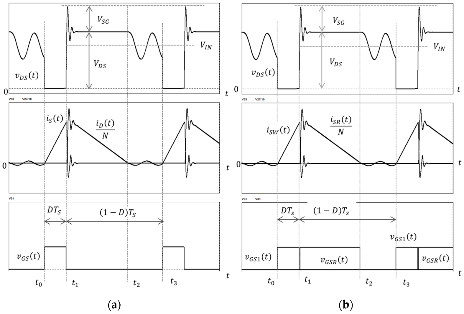
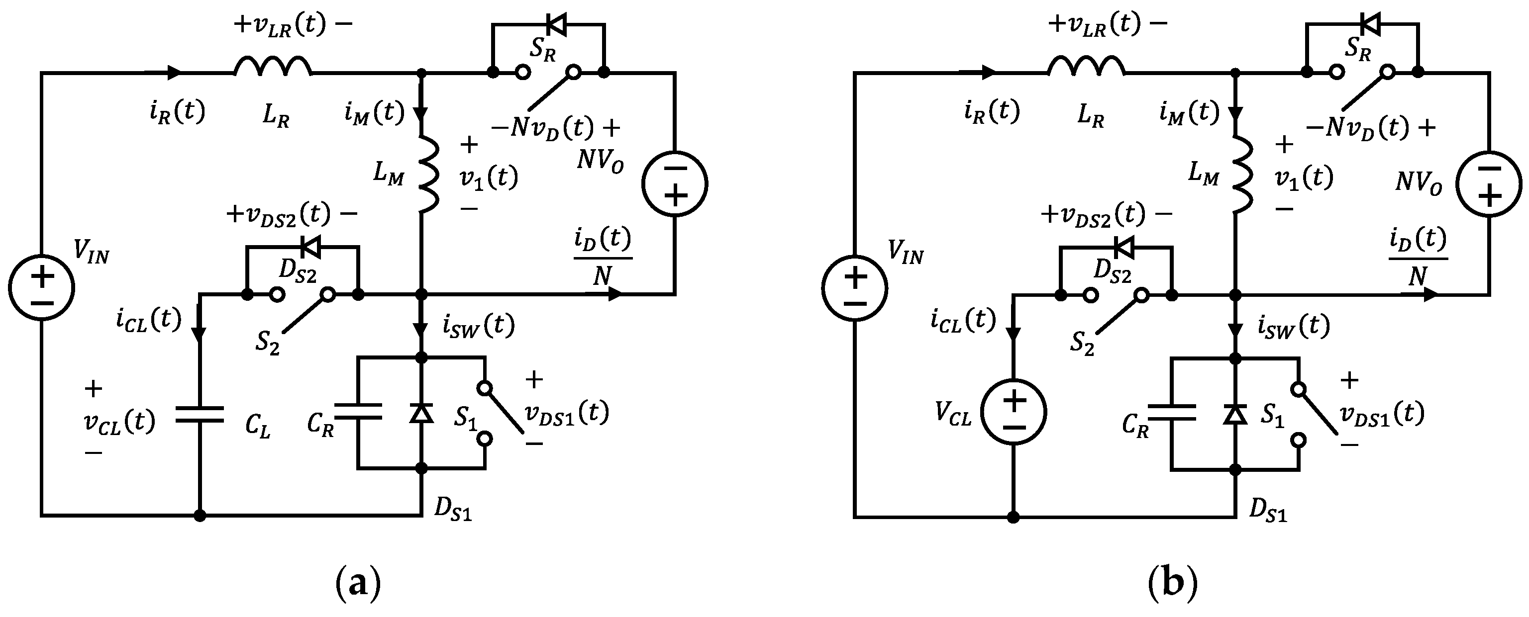
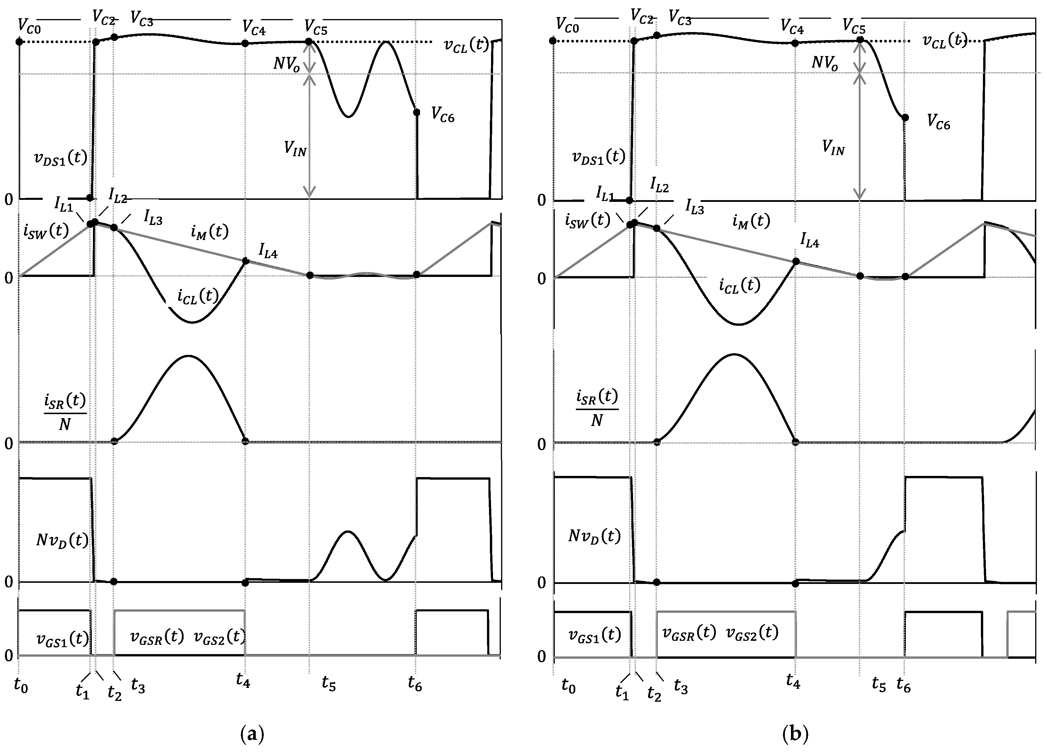
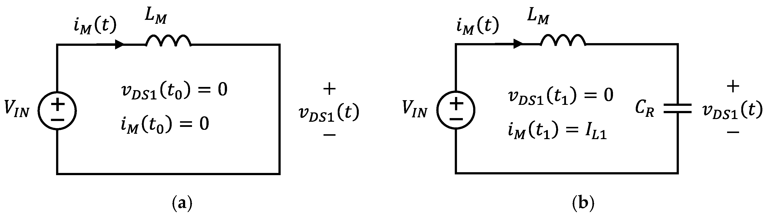
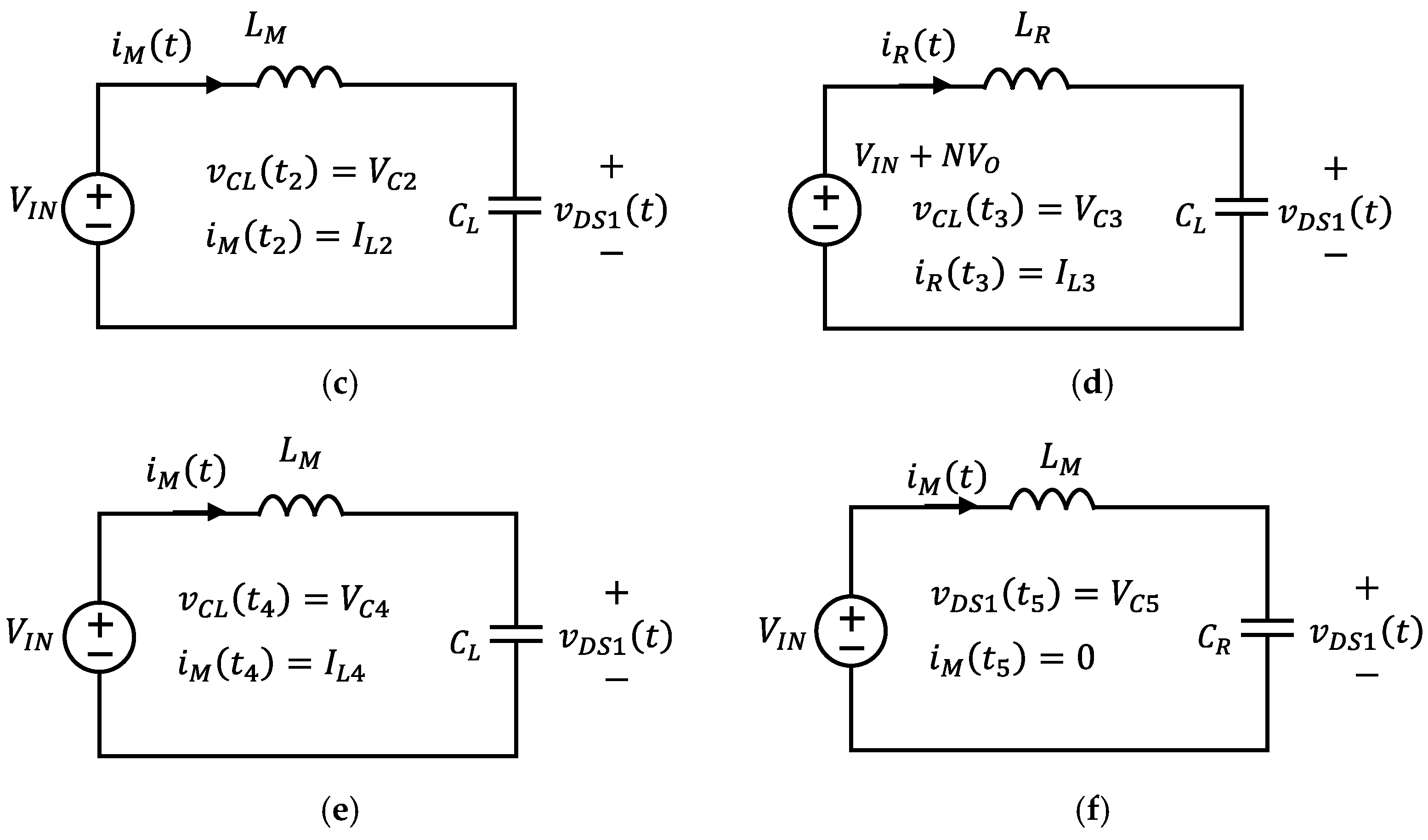
2.2. Steady-State Analysis

Figure 5 shows the operating waveform for the equivalent circuit in Figure 4. Figure 5a shows the switch voltage of the converter turned on in the second valley, whereas Figure 5b shows the switch voltage turned on in the first valley. As can be seen, when the converter operates in a steady state, its state is divided into six operating states for one cycle. In this case, the turn-off timing of the switch is different, but the waveform for each state is the same. The operation mechanism in each state of the converter operating under a steady state is described below [18,19].
First, in state 1, the main switch S 1 is turned on at time t 0 , the secondary-side current of the transformer becomes zero, and the auxiliary switch S 2 and the synchronous rectifier switch S R are turned off. The equivalent circuit of state 1 is shown in Figure 6. As can be seen in Figure 5 and Figure 6, the input voltage is applied to the magnetizing inductor L M and the leakage inductor L K , and the current constantly increases from zero, as shown in Equation (1). Assuming that the main switch voltage is equal to that in Equation (2), and the clamp capacitance is large, the clamp voltage is equal to the turn-off steady-state voltage of the main switch shown in Equation (3). The switch voltage of the synchronous rectifier is determined using Equation (4), and the current is determined with Equation (5). When the main switch S 1 is turned off at time t 1 , the magnetizing current i M becomes I L 1 , and state 1 ends [20,21].
i s w ( t ) = i M ( t ) = i R ( t ) = ( V I N L R + L M ) t
v D S 1 ( t ) = 0
v C L ( t ) = V C 0 = V I N + N V o
N v D ( t ) = ( V I N + N V o )
i S R ( t ) N = 0
When the main switch S 1 is turned off at time t 1 , state 2 starts, and the equivalent circuit is shown in Figure 7. At time t 1 , the initial value of the magnetizing current i M is I L 1 , and the magnetizing inductor L M and the switch equivalent capacitor C R resonate, as shown in Equation (6). The switch resonant voltage is determined with Equation (7). At this time, the characteristic impedance Z r and the resonant angular velocity ω r are calculated using Equation (8). When the resonance voltage of the main switch S 1 becomes equal to the clamp capacitor voltage V C L , the time becomes t 2 , the maximum value of the magnetizing current i M becomes I L 2 , and state 2 ends.
i M ( t ) = i R ( t ) = ( V I N Z r ) sin ω r t + I L 1 cos ω r t
v D S 1 ( t ) = I L 1 Z r sin ω r t + V I N ( 1 cos ω r t )
Z r = L M C R       ω r = 1 L M C R
At time t 2 , when the magnetizing current L M flows through the internal diode of the clamp switch, state 3 starts, and the equivalent circuit in this state is shown in Figure 8. At time t 2 , the initial value of magnetizing current L M is I L 2 , the magnetizing inductor L M and the clamp capacitor C L resonate, and the magnetizing current i M is determined with Equation (9). The clamp capacitor resonant voltage is provided by Equation (10). At this time, the characteristic impedance Z R and the resonant angular velocity ω R are determined using Equation (11). When the clamp current i C L becomes larger than the magnetizing current i M , the magnetizing current becomes I L 3 , the time becomes t 3 , and state 3 ends.
i C L ( t ) = i M ( t ) = i R ( t ) = ( V I N V C 2 Z R ) sin ω R t + I L 2 cos ω R t
v C L ( t ) = I L 2 Z R sin ω R t + V I N ( 1 cos ω R t ) + V C 2
Z R = L M C L     ω R = 1 L M C L
At time t 3 , as the resonance current of the clamp current i C L becomes larger than the magnetizing current i M , the remaining current flows through the rectifier on the secondary side of the transformer. When the synchronous rectifier switch S R and the clamp auxiliary switch S 2 are turned on with the rectifier current, state 4 starts, and the equivalent circuit in this state is shown in Figure 9. At time t 3 , the initial value of the resonance current i C L is I L 3 , the leakage inductor L K and the clamp capacitor C L resonate, and the clamp capacitor current is as shown in Equation (12). The clamp capacitor resonant voltage is calculated using Equation (13). The secondary-side current starts at zero due to resonance and performs zero-current switching (ZCS); thus, its waveform is a sinusoidal wave reflecting the resonance. At this time, the characteristic impedance Z O and the resonant angular velocity ω O are expressed in Equation (15). When the magnetization current i M and the clamp capacitor current i C L become equal, the secondary rectifier current becomes zero, and the time becomes t 4 , and state 4 ends [22,23].
i C L ( t ) = i R ( t ) = ( V I N + N V O V C 3 Z o ) sin ω o t + I L 3 cos ω o t
v C L ( t ) = I L 3 Z o sin ω o t ( V I N + N V O V C 3 ) cos ω o t + ( V I N + N V O )
i S R ( t ) N = I L 3 ( 1 cos ω o t ) N V o L M t ( V I N + N V O V C 3 Z o ) sin ω o t
Z o = L R C L         ω o = 1 L R C L
At time t 4 , the magnetizing current i M and the clamp current i C L become equal, the secondary rectifier current becomes zero, and state 5 begins. The equivalent circuit in this state is shown in Figure 10. When the synchronous rectifier switch S R and the clamp auxiliary switch S 2 are turned off with the rectifier current, the initial value of the resonance current i C L is I L 4 at time t 4 . The magnetizing inductor L M and the clamp capacitor C L resonate, as shown in the figure, and the clamp capacitor current is calculated with Equation (16). The clamp capacitor resonant voltage is calculated using Equation (17). At this time, the characteristic impedance Z R and the resonant angular velocity ω R are expressed in Equation (18). When the magnetizing current i M and the clamp current i C L become zero, the time becomes t 5 , and state 5 ends.
i C L ( t ) = i M ( t ) = i R ( t ) = ( V I N V C 4 Z R ) sin ω R t + I L 4 cos ω R t
v C L ( t ) = I L 4 Z R sin ω R t + V I N ( 1 cos ω R t ) + V C 4
Z R = L M C L           ω R = 1 L M C L
At time t 5 , when the magnetizing current i M , the clamp current i C L , and the secondary rectifier current become zero, state 6 starts, and its equivalent circuit is shown in Figure 11. At time t 5 , the initial value of the turn-off voltage of the main switch is V C 5 , and the magnetizing inductor L M and the switch equivalent capacitor C R resonate, as shown in the figure. The magnetizing current is determined using Equation (19), and the switch resonant voltage is expressed in Equation (20). At this time, the characteristic impedance Z r and the resonant angular velocity ω r are found using Equation (21). When the switch voltage reaches the lowest point V C 6 due to resonance, it becomes time t 6 , and at this time, if the switch is turned on by the control circuit, the turn-on loss can be minimized.
Figure 12 shows a simplified resonant equivalent circuit with the components constituting the resonant circuit for each state equivalent circuit. The initial current and voltage values for each resonant equivalent circuit are shown [24,25].
i M ( t ) = i R ( t ) = i S W ( t ) = ( V I N V C 5 Z r ) sin ω r t
v D S 1 ( t ) = ( V C 5 V I N ) cos ω r t + V I N
Z r = L M C R           ω r = 1 L M C R
To find the appropriate value of the clamp capacitor, the voltage of the magnetizing inductor L M is obtained using Equation (22). During states 4 and 5, the voltage value is N V o , and the maximum current value is I M + . Assuming that the time of state 2–5 is twice the resonance time of the leakage inductor L K and the clamp capacitor C L , Equation (23) is used. The clamp capacitor value can be obtained from Equation (24). At this time, the maximum voltage value of the clamp capacitor is determined using Equation (25).
v M ( t ) = L M d i M ( t ) d t
N V o = L M ( I M + 2 × 2 π L K C L )
C L = 1 L K ( L M I M + 4 π N V o ) 2
V C L = V I N + N V o

3. Design of QR Flyback DC–DC Converter with SDAS

3.1. Optimal Design Process for Major Devices

The electrical specifications shown in Table 1 were determined for the design of the SDAS-applied QR flyback converter proposed in this paper. The input voltage was AC 90–264 V, the output voltage was set at 12 V, and the maximum output was set at 60 W. Since the AC–DC power supply of less than 75 W is not subject to the IEC 61000-3-2 limitation of current harmonics, the PFC circuit was not used. The size of the power supply device was 29 mm in width, 23 mm in height, and 74 mm in length, and the volume at this time was less than 50 cc.
The winding ratio of the transformer is calculated with Equation (26), and V c is the voltage that is converted from the output voltage to the primary-side voltage. K c is the design margin coefficient. In this design, the secondary winding of the transformer was determined as the minimum natural number, so 5 was selected. Since the QR flyback converter always operates in a discontinuous current mode, the entire energy stored in the magnetizing inductor L M is delivered to the output   P o . Therefore, the magnetizing inductor L M is expressed using Equation (26). The maximum duty rate d m a x appears at the lowest input voltage and is shown in Equation (28). The RMS values of the current in the primary and secondary windings of the transformer are determined with Equations (29) and (30). Equation (24) can be used for the clamp capacitor, and the result is shown in Equation (31). For the clamp capacitor value, 68 nF was selected, which is the closest standard value [26,27,28,29,30].
N = N 1 N 2 = K c V c V o = 1.5 × 50 12 = 6.3
L M = 2   P o I R 2   f s w = 2 × 70 2.5 2 × 83 k = 260     μ H
d m a x = I p k L M f s w V I N   m i n = 2.5 × 269 μ × 83 k 90 2 = 0.42
I 1   r m s = I p k d m a x 3 = 2.5 0.42 3 = 0.94   A
I 2   r m s = N I p k 1 d m a x 3 = 2.5 × 6.3 1 0.42 3 = 6.93   A
C L = 1 5.3 μ ( 260 μ × 2.5 4 π × 6.4 × 13 ) 2 = 73   nF

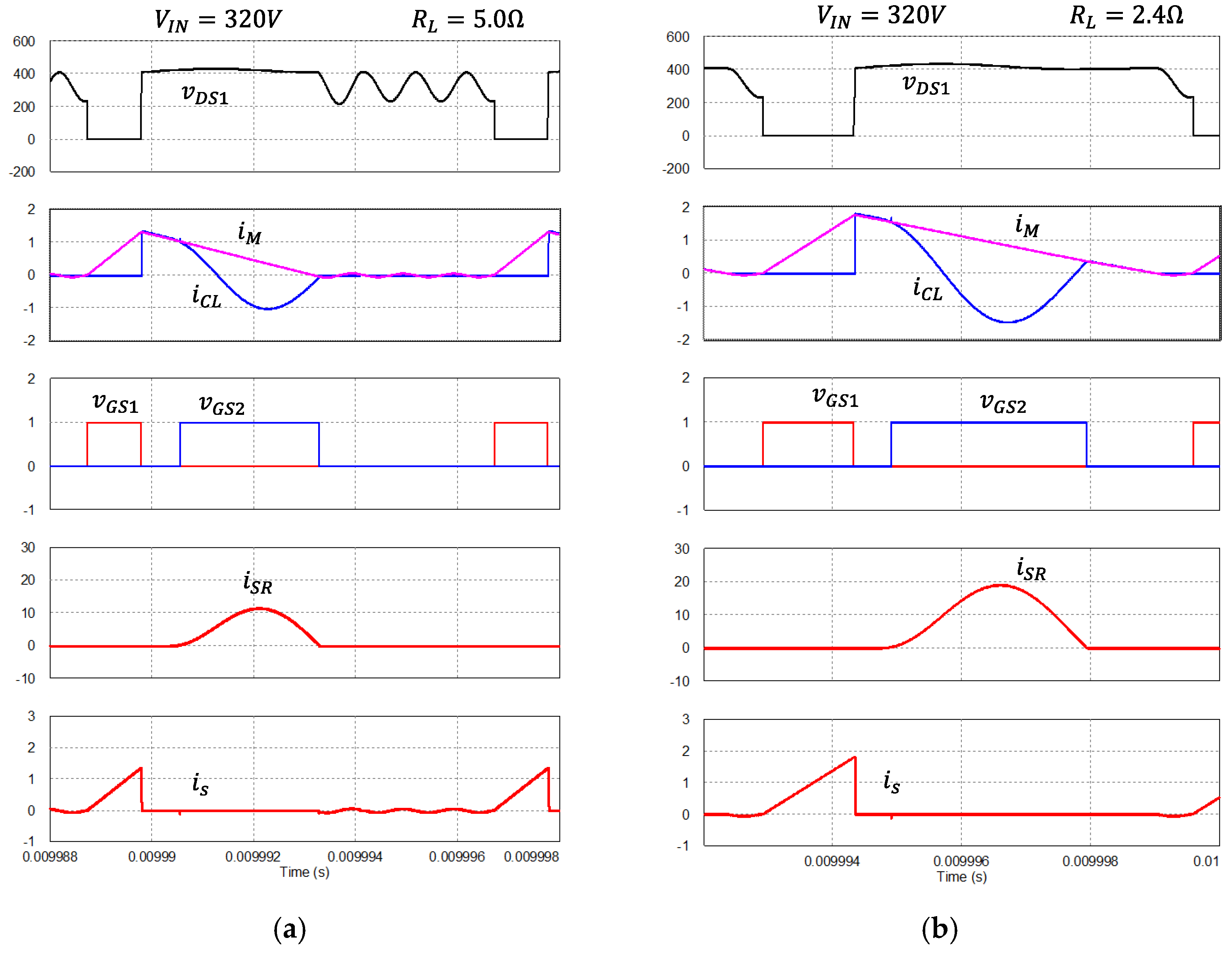
3.2. Circuit Simulation Results

To verify the design results of the QR flyback converter using the SDAS designed in the previous section, a circuit simulation was performed using PSIM 11.0, and the simulation circuit diagram is shown in Figure 13. In the figure, the previously designed values were used for the main components of the converter, and the main switches and transformers were modeled as ideal components. To stabilize the output voltage, a valley-switching PWM control circuit suitable for the QR flyback converter was designed. Figure 14 is the waveform results of the PSIM simulation when the converter operated in a steady state. In Figure 14a, the input voltage was DC 320 V, and the load resistance was 5 Ω; in Figure 14b, the input voltage was DC 320 V, and the load resistance was 2.4 Ω. These values correspond to approximately 30 W and 60 W of output power [31].
In the figure, shown from the top, the operating waveforms refer to the main switch voltage v D S 1 , the magnetizing inductor current i M , the clamp capacitor current i C L , the switch drive voltage v G S 1 , 2 , the transformer secondary rectifier current i S R , and the switch current i S . As can be seen from this figure, when the DC input voltage was 320 V, the switch was turned on at the lowest point of the valley. As the power load increased, the number of valleys decreased, and the switch was turned on in the first valley at full load. The driving voltage of the clamp and the synchronous rectifier switch was controlled by the secondary-side rectifier current of the transformer [32]. As a result, it can be seen that the SDAS circuit consisting of the clamp switch and the clamp capacitor operated properly, and the voltage surge was eliminated during the turn-off period of the main switch. Specifically, the rectifier current on the secondary side of the transformer is in the form of a half-wave rectified sinusoidal wave occurred by the resonance, and it showed ZCS characteristics and reduced the switching loss and voltage surge, lowering the rectifier voltage rating [33,34].
In Figure 15, the PSIM simulation results are compared with the experimental results when a 60 W class QR flyback converter with the SDAS was used under a steady state. Shown from the top, the operating waveforms refer to the switch drive voltage v G S 1 , the main switch voltage v D S 1 , the switch current i s , the clamp capacitor current i C L , the transformer secondary rectifier current i S R , the clamp switch drive voltage v G S 2 , the clamp capacitor voltage v C L , and the transformer primary voltage v 1 . It can be seen that the PSIM simulation results and the experimental waveforms are in relatively good agreement, and they are the same as the operation of each state described above. Therefore, it was confirmed that both the analysis of the steady-state operation and the design process were valid [35].

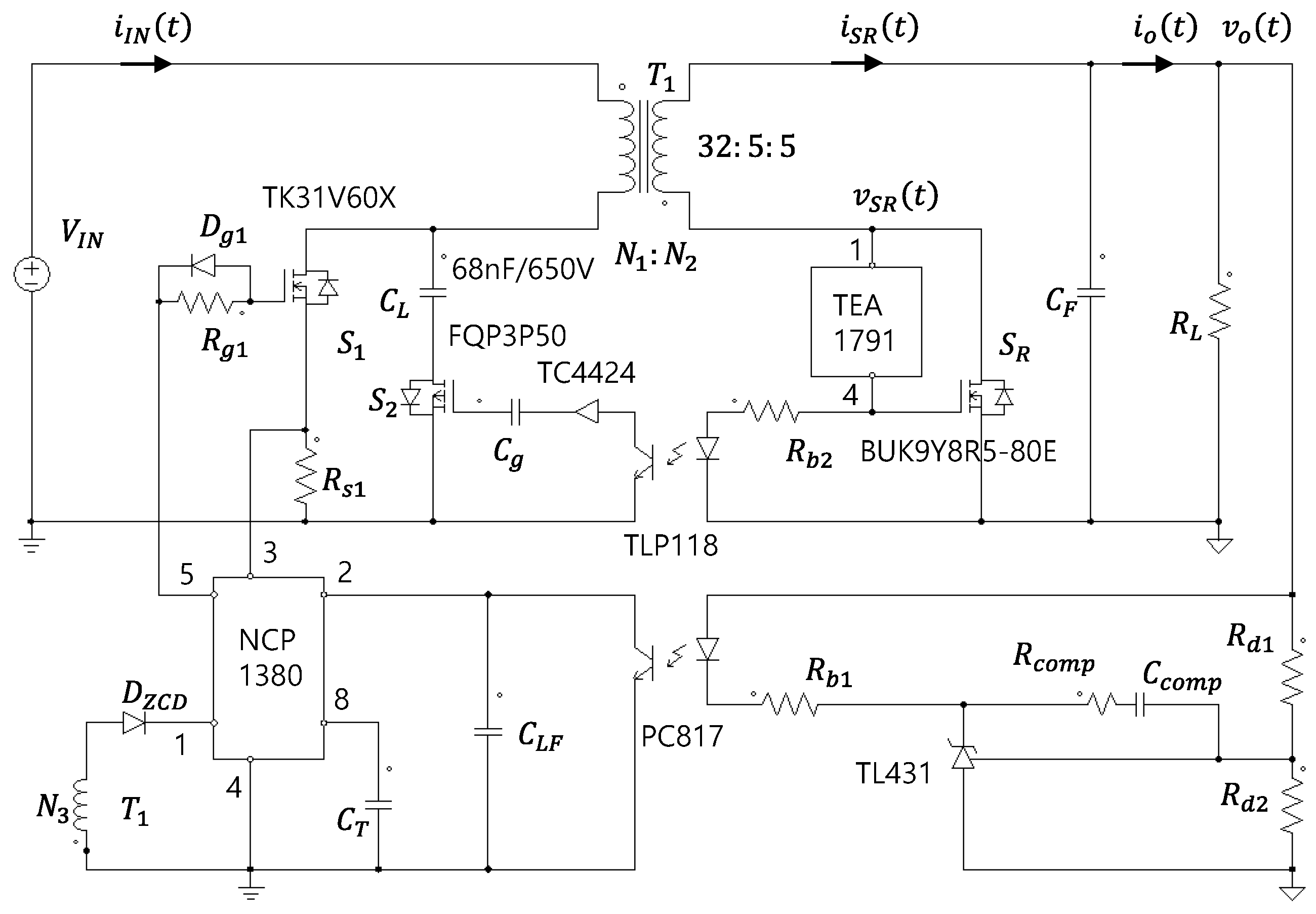
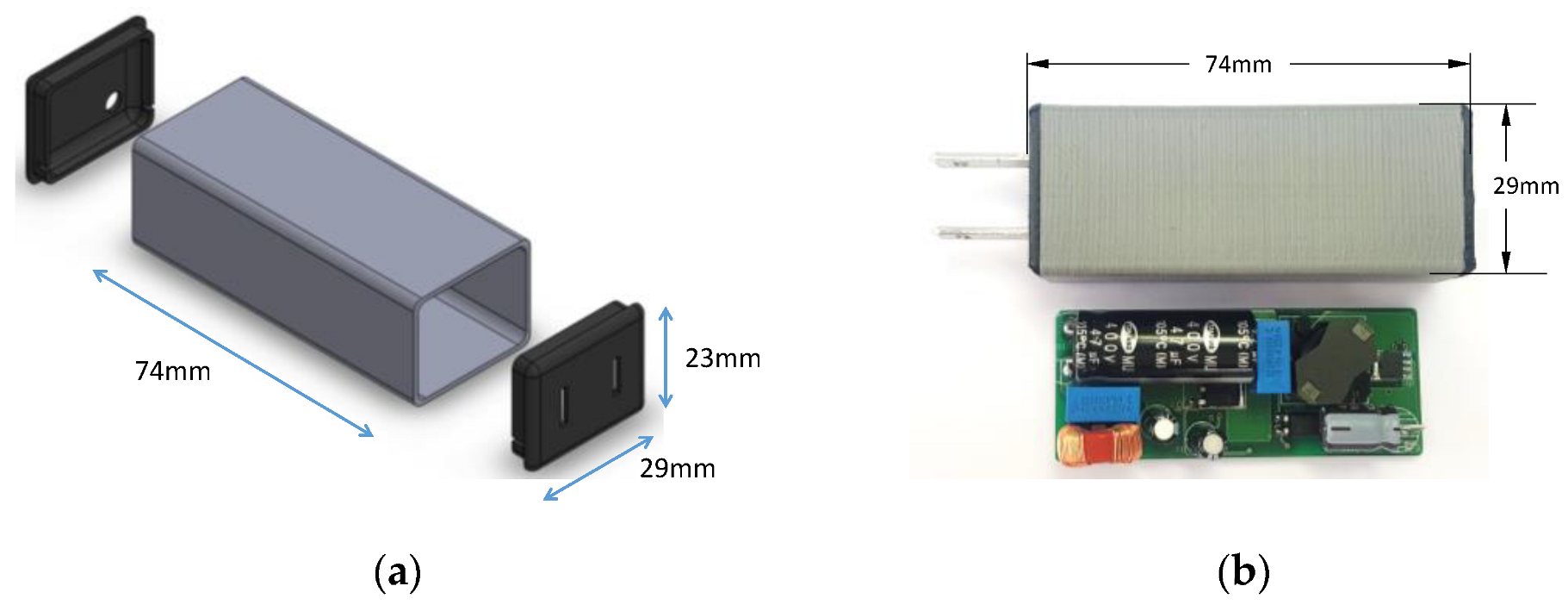
3.3. Compact AC–DC Adapter Design

Figure 16 shows the basic structure including the control circuit to construct the AC–DC adapter designed above. The basic circuit in the figure is for a QR flyback converter with the SDAS composed of existing commercialized QR flyback control components and an isolation circuit using a photocoupler. As shown in Figure 16, a synchronous rectifier driver component was used to control the synchronous rectifier switch S R , and a photo driver was used to deliver a driving signal to the clamp switch S 2 on the primary side of the transformer. As a result, the operation of the synchronous rectifier and the clamp switch was always the same [36,37].
Table 2 shows the main components and their electrical characteristics constituting the experimental AC–DC adapter circuit. For the main switch, a MOSFET with a relatively low voltage rating of 600 V was used, as it could reduce the on-resistance compared with other MOSFETs with a similar current rating. A 500 V class P-channel MOSFET was used for the clamp switch and a surface-mounted device (SMD) MOSFET with 6.3 mΩ on-resistance was used for the synchronous rectifier switch to minimize the conduction loss. A QR flyback control IC, NCP1380, was used to control the main switch, TEA1791 was used as the synchronous rectifier driver, and TLP118 was used as the photo driver. Table 3 shows the characteristics of the transformer used in the experimental AC–DC adapter circuit. The magnetic core size of the transformer was TDK’s RM7. For the primary winding, Litz wires comprising a bundle of 30 copper wires with 0.1 mm thickness were used to reduce high-frequency loss, and Litz wires comprising 60 copper wires were used for the secondary winding to deal with a large RMS current value. The measured magnetizing inductance was 260 μH, and the leakage inductance was 5.3 μH. The clamp capacitor was a 68 nF film capacitor rated at 650 V. Figure 17 shows the experimental circuit diagram. In the circuit diagram, the AC–DC rectifier was omitted for convenience, but a general full-wave rectifier was applied in the experiment [38,39,40].
Figure 18 shows the external appearance of the experimental AC–DC adapter. Figure 18a is the assembly drawing of the outer case, and Figure 18b is the inside and outside size and shape of the constructed experimental circuit. The AC–DC adapter was a 74 mm long rectangular cylinder case with a hollow inside and a rectangular lid attached to both ends. The AC terminal was integrated with the lid on one side. The volume of the adapter was 50 cc, and the power density was approximately 20   W / in 3 . Figure 19 is the instrument composition and test environment to test the experimental circuit. The power supply used in the experiment was a PCR400LE, the electronic load was a PLZ1004WH from Kikusui (Yokohama, Kanagawa, Japan), the power analyzer was a WT1600 from YOKOGAWA (Tokyo, Japan), and the oscilloscope was an HDO6104 model from LeCroy (Chestnut Ridge, NY, USA). To measure the waveform of the experimental circuit in a steady state, the test was carried out without the case.

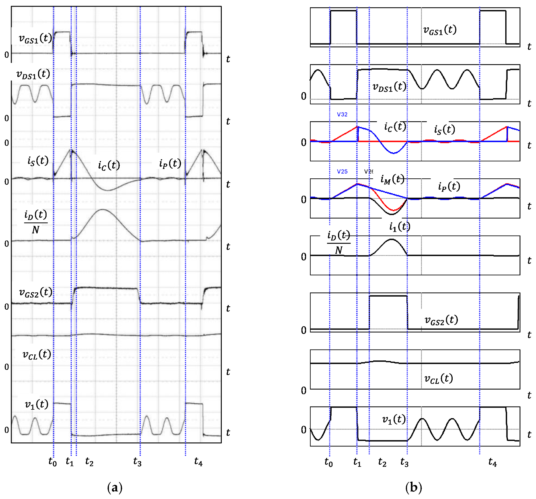
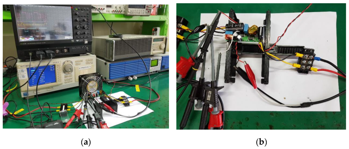
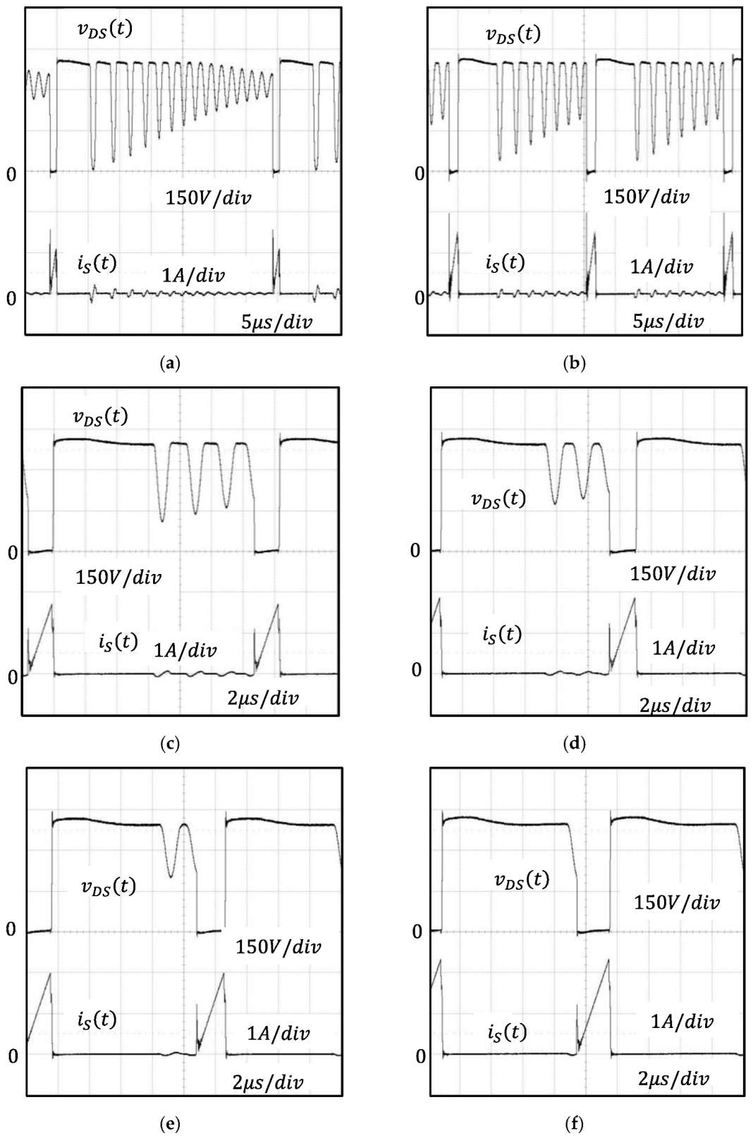
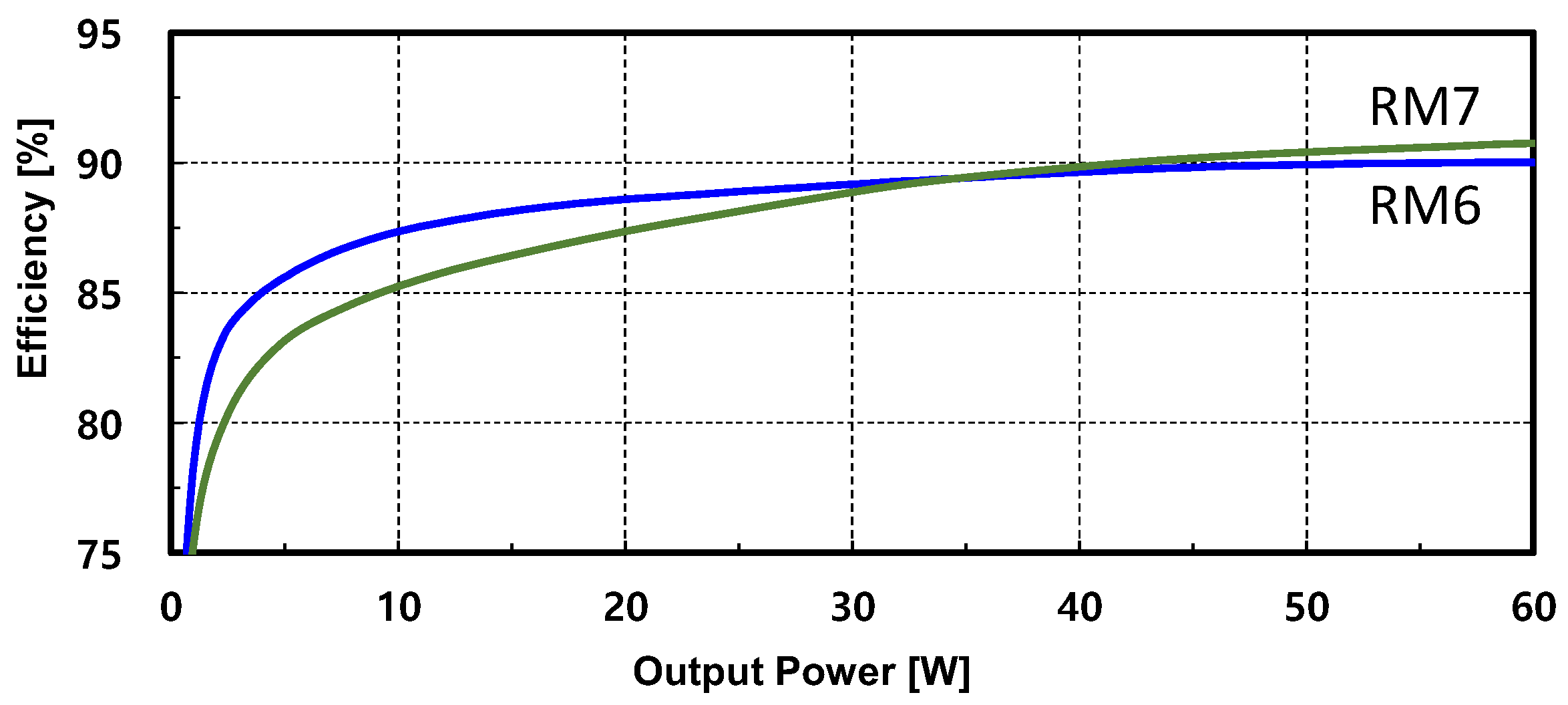
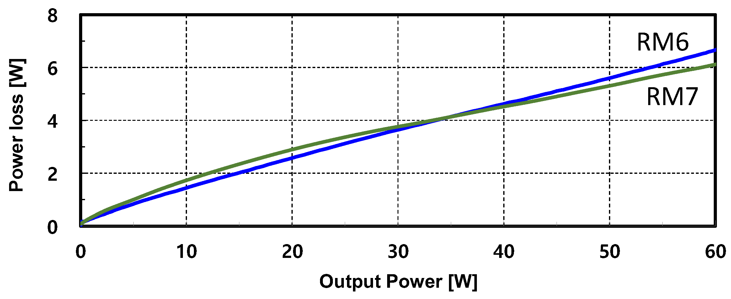
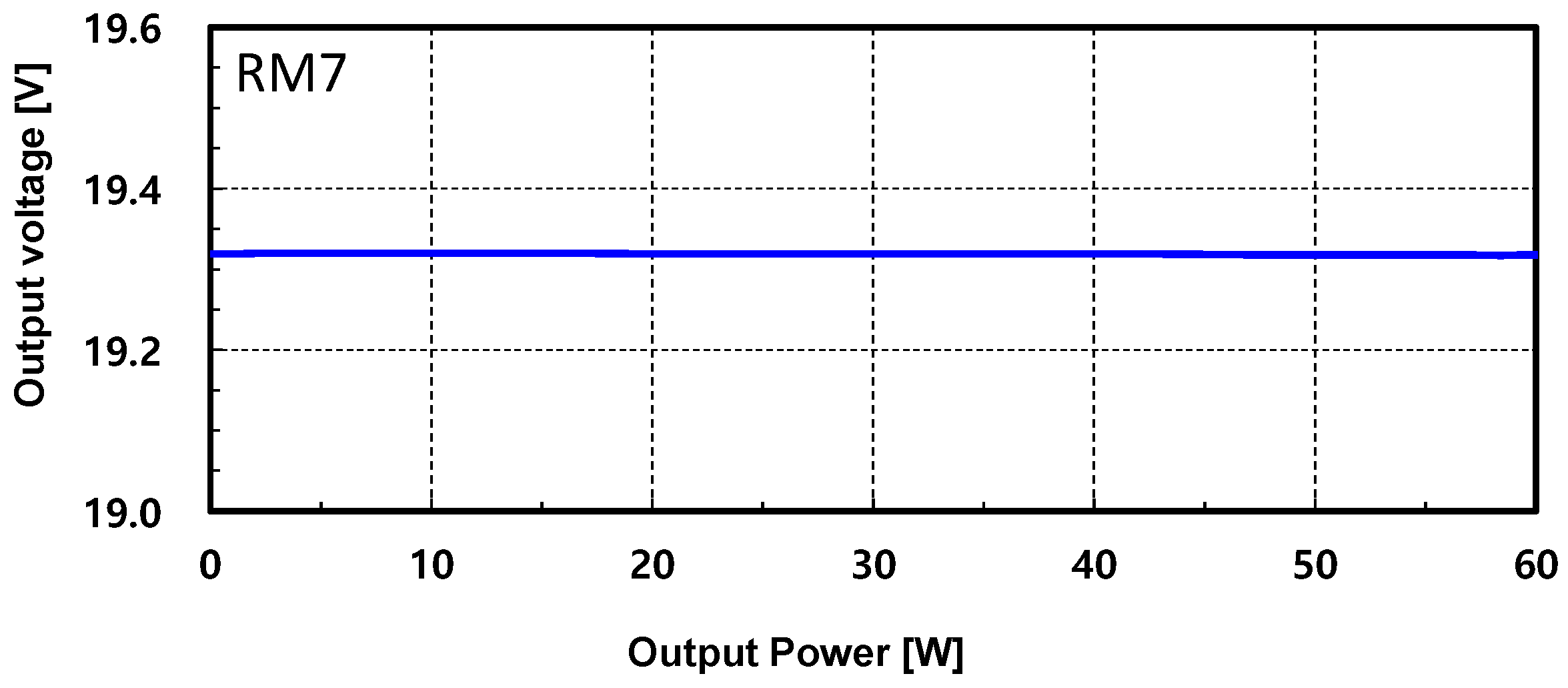
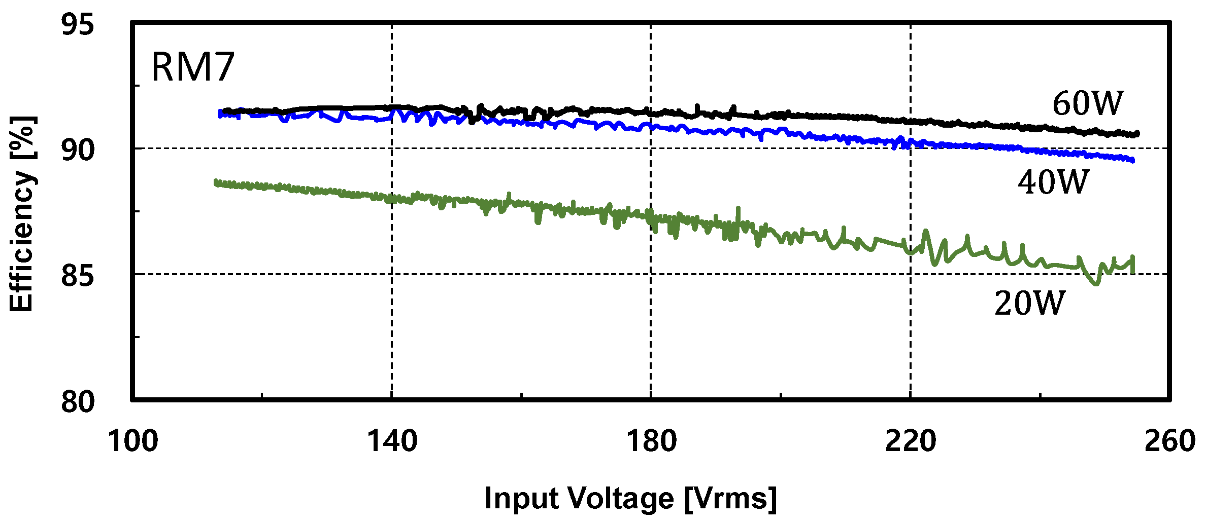
4. Experimental Results

To verify the effectiveness of the QR flyback converter with the SDAS proposed in this paper, a 60 W AC–DC adapter was tested. Figure 20 is the steady-state operating waveform of the experimental circuit when the input voltage was 310 V. In Figure 20a, the output current was 0.3 A, the voltage v D S of the main switch is shown on the top, and the switch current i S is shown on the bottom. The power load was approximately 3.6 W, and the switch voltage showed a small duty cycle under a low load current. At this time, the turn-off voltage of the switch was clamped by the SDAS circuit and limited to 420 V. As the load current increased, the operating waveform changed from Figure 20b to Figure 20f. Figure 20f shows when the load current was 5 A, and the output power was 60 W. The maximum switch current was 2.4 A, and the maximum switch voltage was limited to about 450 V. It can be seen from this figure that depending on the load, the peak value of the switch voltage did not significantly increase and was clamped to a constant level [41].
Figure 21 shows a comparison of the switch voltage and current waveforms of a conventional QR flyback converter and the proposed QR flyback converter with the SDAS. The input voltage was 310 V, the load current was 3.5 A, and the output power was 42 W. Figure 21a shows the switch voltage and current waveforms of the experimental circuit using the existing QR flyback converter and RCD snubber, and Figure 21b is the switch voltage and current waveform of the QR flyback converter with the SDAS. As shown in Figure 21a, the voltage surge of the switch occurred at the turn-off moment and had a peak value of up to 550 V. After that, the voltage surge was limited to about 500 V, there was a damping resonance period, and then the voltage surge stabilized at about 410 V, which was the turn-off steady-state voltage. The switch turned on in the second valley, and the switch current had a peak value of about 2 A. At this time, the switch-turn-off voltage also influenced the current during the damping resonance period, and therefore the current resonated simultaneously. As shown in Figure 21b, the turn-off voltage of the switch was clamped by the SDAS circuit and had a peak value of 430 V, and the peak value of the switch current was about 1.9 A. As can be seen in the figure, compared with the RCD clamp circuit, the SDAS circuit reduced the voltage surge of the QR flyback switch by up to 120 V or more. In addition, compared with RCD snubbers, which consume the voltage surge power in resistors, SDAS circuits do not consume power and, therefore, have higher efficiency characteristics in principle [42].
Figure 22 shows the power conversion efficiency of the experimental circuit at an input voltage of 310 V. The efficiency was over 85% when the output power was more than 5 W, and the efficiency was as high as 90% at the maximum power load of 60 W. Figure 23 shows the internal power dissipation of the adapter. At a power load of 10 W, there was a power loss of approximately 1.5 W, and at a maximum power load of 60 W, an internal loss of 6.7 W was observed. Figure 24 shows the output voltage relative to the power load. As evident in the figure, the output voltage remained stable, and a maximum voltage change of less than 5 mV was observed with the change in power load. Figure 25 shows the power conversion efficiency measured at the output power of 20 W, 40 W, and 60 W relative to the input voltage. The efficiency increased at a higher output and with a decrease in the input voltage. Specifically, the maximum power conversion efficiency was achieved when the input voltage was 140 V, and the output was 60 W, at 91.56%. When the output was 60 W, the power conversion efficiency was over 90% in all rates of input voltage.
These experimental results highlight the following findings: The AC–DC adapter of the proposed QR flyback converter with the SDAS showed a high power density of more than 20   W / in 3 and a high power conversion efficiency of up to 91.56%. Therefore, the proposed SDAS method can be used as the basic circuit method for high-efficiency power supply. One of the reasons for such high efficiency is due to the SDAS circuit, which sufficiently reduces the voltage surge of the QR flyback switch compared with the RCD clamp circuit and does not consume power in principle. Specifically, a separate control circuit is not required to drive the auxiliary switch for the clamp, and the circuit structure is simplified because it is self-driven inside the converter [43].

5. Conclusions

In this paper, a QR flyback converter using a self-driven active snubber (SDAS) was proposed to solve the problem of the switch voltage surge in the QR flyback converter. In the proposed converter, the SDAS consisting of a clamping capacitor and an active switch was configured in parallel with the main switch or transformer to reduce the voltage surge in the switch. The clamp switch was synchronized with the drive signal of an internal synchronous rectifier and a photo driver or pulse transformer, so no separate control circuit was required.
To confirm the steady-state characteristics of the proposed QR flyback converter with SDAS, equivalent circuits for each state were constructed, and the equations and characteristics for each state were determined. Using the main components for each state, the resonant circuit was separately arranged, and the components involved in resonance and the initial values of each state were identified. The values of the main elements were designed using the steady-state analysis results, and the optimal values of the clamp capacitor were derived. To compare the steady-state analysis results, a simulation using the PSIM program was performed. The simulation results and the theoretical waveforms were relatively well matched, and they showed a very similar shape to the experimental waveforms.
To confirm the effectiveness of the proposed converter and control circuit method, a 60 W class small AC–DC adapter was constructed, and the experimental results were presented. The size of the experimental AC–DC adapter was 74 × 29 × 23   mm and had a high power density of 20   W / in 3 or more. The experimental circuit was limited to the high power conversion efficiency of up to 91.56%, and the maximum voltage surge of the switch was approximately 450 V. Taken together, these results highlight the applicability of the proposed converter as the basic circuit method for achieving high-efficiency power supply. One of the reasons for such high efficiency is due to the SDAS circuit, which sufficiently reduces the voltage surge of the QR flyback switch compared with the RCD clamp circuit and does not consume power in principle.

Author Contributions

Conceptualization, T.-Y.A. and J.-O.B.; Methodology, J.-S.Y., J.-O.B. and T.-Y.A.; Validation, J.-S.Y., J.-O.B. and T.-Y.A.; Formal analysis, T.-Y.A.; Investigation, J.-S.Y. and J.-O.B.; Resources, T.-Y.A.; Data curation, J.-O.B. and T.-Y.A.; Writing—original draft preparation, J.-S.Y., J.-O.B. and T.-Y.A.; Writing—review and editing, J.-S.Y., J.-O.B. and T.-Y.A.; Visualization, J.-S.Y. and T.-Y.A.; Supervision, J.-O.B. and T.-Y.A.; Project administration, J.-O.B. and T.-Y.A.; Funding acquisition, T.-Y.A. All authors have read and agreed to the published version of the manuscript.

Funding

This work was supported by the Technological Innovation R&D Program (S3106696, Distributed power smart grid conversion module with GaN power semiconductor) funded by the Ministry of SMEs and Startups (MSS, Republic of Korea).

Data Availability Statement

Not applicable.

Conflicts of Interest

The authors declare no conflict of interest.

References

  1. Park, H.-P.; Jung, J.-H. Design Methodology of Quasi-Resonant Flyback Converter with a Divided Resonant Capacitor. IEEE Trans. Ind. Electron. 2020, 68, 10796–10805. [Google Scholar] [CrossRef]
  2. Wang, C.; Xu, S.; Shen, W.; Lu, S.; Sun, W. A Single-Switched High-Switching-Frequency Quasi-Resonant Flyback Converter. IEEE Trans. Power Electron. 2018, 34, 8775–8786. [Google Scholar] [CrossRef]
  3. Baek, J.-O. A Study on New Active Clamp Circuit and Control Method for High Efficiency Quasi Resonant Flyback Converter. Ph.D. Thesis, Cheongju University, Graduate School of Cheongju University, Cheongju, Republic of Korea, 2018. [Google Scholar]
  4. Wang, J.-M.; Lin, C.-W.; Huang, K.-Y.; Wong, J.-S. The Novel Quasi-Resonant Flyback Converter with Autoregulated Structure for Parallel/Serial Input. IEEE Trans. Ind. Electron. 2019, 67, 992–1004. [Google Scholar] [CrossRef]
  5. Mauromicale, G.; Raciti, A.; Rizzo, S.A.; Susinni, G.; Fusillo, F.; Palermo, A.; Scrimizzi, F.; Scollo, R. Si and GaN Devices in Quasi Resonant Flyback converters for Wall Charger Applications. In Proceedings of the 2019 IEEE Energy Conversion Congress and Exposition (ECCE), Baltimore, MD, USA, 29 September–3 October 2019. [Google Scholar] [CrossRef]
  6. Halil, O.; Sueel, V.; Hava, A. A comprehensive loss analysis of quasi resonant flyback converter for design purpose. In Proceedings of the PCIM Asia 2018 International Exhibition and Conference for Power Electronics, Intelligent Motion, Renewable Energy and Energy Management, Shanghai, China, 26–28 June 2018. [Google Scholar]
  7. Xu, S.; Wang, C.; Qian, Q.; Zhu, J.; Sun, W.; Li, H. A single-switched high-switching-frequency quasi-resonant flyback converter with zero-current-switching and valley-switching. In Proceedings of the 2019 IEEE Applied Power Electronics Conference and Exposition (APEC), Anaheim, CA, USA, 17–21 March 2019. [Google Scholar] [CrossRef]
  8. Min, G.-H.; Ha, J.-I. Inner Supply Data Transmission in Quasi-Resonant Flyback Converters for Li-Ion Battery Applications Using Multiplexing Mode. IEEE Trans. Power Electron. 2018, 34, 64–73. [Google Scholar] [CrossRef]
  9. Cheng, M.; Liu, L.; Liao, Z.; Yu, J.; Peng, S.; Zhang, Z.; Ye, T.; Wang, N. On Silicon-Integrated Micro-Transformers and Their Applications in Quasi-Resonant Flyback Converters. IEEE Trans. Magn. 2022, 58, 8401209. [Google Scholar] [CrossRef]
  10. Kang, B.; Low, K.-S.; Ng, K.J. Capacitor Charging by Quasi-Resonant Approach for a Pulsed Plasma Thruster in Nano-Satellite. IEEE Trans. Plasma Sci. 2020, 48, 1271–1278. [Google Scholar] [CrossRef]
  11. Vračar, D.; Pejovic, P.V. Active-Clamp Flyback Converter as Auxiliary Power-Supply of an 800 V Inductive-Charging System for Electric Vehicles. IEEE Access 2022, 10, 38254–38271. [Google Scholar] [CrossRef]
  12. Yao, J.; Li, Y.; Wang, S.; Huang, X.; Lyu, X. Analysis and Reduction of Radiated EMI in High-Frequency GaN IC-based Active Clamp Flyback Converters. In Proceedings of the 2020 IEEE Applied Power Electronics Conference and Exposition (APEC), New Orleans, LA, USA, 15–19 March 2020. [Google Scholar] [CrossRef]
  13. Wang, C.; Sun, D.; Zhang, X.; Hu, J.; Gu, W.; Gui, S. A Constant Current Digital Control Method for Primary-Side Regulation Active-Clamp Flyback Converter. IEEE Trans. Power Electron. 2020, 36, 7307–7318. [Google Scholar] [CrossRef]
  14. Kuo, C.-C.; Lee, J.-J.; He, Y.-H.; Wu, J.-Y.; Chen, K.-H.; Lin, Y.-H.; Lin, S.-R.; Tsai, T.-Y. A dynamic resonant period control technique for fast and zero voltage switching in GaN-based active clamp flyback converters. IEEE Trans. Power Electron. 2020, 36, 3323–3334. [Google Scholar] [CrossRef]
  15. Xue, L.; Zhang, J. Design considerations of highly-efficient active clamp flyback converter using GaN power ICs. In Proceedings of the 2018 IEEE Applied Power Electronics Conference and Exposition (APEC), San Antonio, TX, USA, 4–8 March 2018. [Google Scholar] [CrossRef]
  16. Hu, J.; Wen, B.; Burgos, R.; Kang, Y. Design of a Wide-Input-Voltage PCB-Embedded Transformer Based Active-Clamp Flyback Converter Considering Permeability Degradation. IEEE Trans. Power Electron. 2021, 36, 10355–10365. [Google Scholar] [CrossRef]
  17. Ma, Z.; Yao, J.; Wang, S.; Sheng, H.; Lakshmikanthan, S.; Osterhout, D. Radiated EMI Reduction with Double Shielding Techniques in Active-clamp Flyback Converters. In Proceedings of the 2021 IEEE International Joint EMC/SI/PI and EMC Europe Symposium, Raleigh, NC, USA, 26 July–13 August 2021. [Google Scholar] [CrossRef]
  18. Wu, S.-T.; Cheng, Y.-T. Design and Implementation of a Single-Stage PFC Active-Clamp Flyback Converter with Dual Transformers. Electronics 2021, 10, 2588. [Google Scholar] [CrossRef]
  19. Chen, M.; Xu, S.; Huang, L.; Sun, W.; Shi, L. A Novel Digital Control Method of Primary-Side Regulated Flyback with Active Clamping Technique. IEEE Trans. Circuits Syst. I Regul. Pap. 2020, 68, 950–962. [Google Scholar] [CrossRef]
  20. Xu, S.; Qian, Q.; Tao, T.; Lu, S.; Sun, W. Small Signal Modeling and Control Loop Design of Critical Conduction Mode Active Clamp Flyback Converter. IEEE Trans. Power Electron. 2020, 36, 7250–7263. [Google Scholar] [CrossRef]
  21. Nasiri, A.; Banaei, M.R.; Abadi, A.S.S. Phase-shifted active clamp flyback converter for driving a magnetron. In Proceedings of the 2019 27th Iranian Conference on Electrical Engineering (ICEE), Yazd, Iran, 30 April–2 May 2019. [Google Scholar]
  22. Nasiri, A.; Abadi, A.S.S. A New Driving Method for a Magnetron Using a Soft Switching Active Clamp Fly-back Converter. In Proceedings of the 2019 10th International Power Electronics, Drive Systems and Technologies Conference (PEDSTC), Shiraz, Iran, 12–14 February 2019. [Google Scholar] [CrossRef]
  23. Li, H.; Li, S.; Xiao, W.; Hui, S.Y.R. A Modulation Method for Capacitance Reduction in Active-Clamp Flyback-Based AC–DC Adapters. IEEE Trans. Power Electron. 2022, 37, 9455–9467. [Google Scholar] [CrossRef]
  24. Gao, S.; Song, H.; Wang, Y.; Xu, R.; Xu, D. A Secondary-Resonance MHz Active-Clamp Flyback Converter with Partial Power Processing. IEEE Trans. Ind. Appl. 2022, 58, 7988–7997. [Google Scholar] [CrossRef]
  25. Gu, D.; Xi, J.; He, L. Digitally controlled GaN-based MHz active clamp flyback converter with dynamic dead time optimisation for AC–DC adapter. IET Power Electron. 2020, 13, 3777–3786. [Google Scholar] [CrossRef]
  26. Xu, S.; Qian, Q.; Ren, B.; Liu, Q. An accurate small signal modeling and control loop design of active clamp flyback converter. In Proceedings of the 2019 10th International Conference on Power Electronics and ECCE Asia (ICPE 2019-ECCE Asia), Busan, Republic of Korea, 27–30 May 2019. [Google Scholar]
  27. Tang, C.-Y.; Lin, W.-Z.; Tan, Y.-C. An Active Clamp Flyback Converter with High Precision Primary-Side Regulation Strategy. IEEE Trans. Power Electron. 2022, 37, 10281–10289. [Google Scholar] [CrossRef]
  28. Xu, S.; Qian, Q.; Shi, R.; Shah, S.S.; Liu, Q.; Lu, S.; Sun, W. Sampled-Data Modeling for PCM and ZVS Controlled Critical Conduction Mode (CrCM) Active Clamp Flyback (ACF) Converter at Variable Switching Frequency. IEEE Trans. Circuits Syst. I: Regul. Pap. 2020, 67, 3588–3600. [Google Scholar] [CrossRef]
  29. Liu, Y.-C.; Huang, B.-S.; Lin, C.-H.; Kim, K.A.; Chiu, H.-J. Design and implementation of a high power density active-clamped flyback converter. In Proceedings of the 2018 International Power Electronics Conference (IPEC-Niigata 2018-ECCE Asia), Niigata, Japan, 20–24 May 2018. [Google Scholar]
  30. Zaman, A.; Radic, A. How to Design and Implement an Adapter Power Supply with Active Clamp Flyback: An All Silicon Design Methodology. IEEE Power Electron. Mag. 2020, 7, 36–43. [Google Scholar] [CrossRef]
  31. Dey, S.; Ray, M.B.; Soni, H.; Ghosh, R.; Shah, M. Comparison between Quasi-Resonant and Active Clamp Flyback topologies for GaN-based 65 W Wall Charger Application. In Proceedings of the 2021 IEEE Applied Power Electronics Conference and Exposition (APEC), Phoenix, AZ, USA, 14–17 June 2021. [Google Scholar]
  32. Hosseinabadi, F.; Soleymani, B.; Adib, E.; Islam, R.; Farzanehfard, H.; Kouzani, A.Z.; Mahmud, M.A.P. A soft-switching inverting high step-down converter with a pair of coupled inductors and self-driven synchronous rectifier. IET Power Electron. 2021, 14, 2441–2451. [Google Scholar] [CrossRef]
  33. Mahdi, G.J.; Allahyari, H.; Shoaei, A.; Adib, E.; Bahrami, H.; Zadeh, M.A.L.; Fahimifar, M.H. A self-driven synchronous rectification wide-range ZVS single-switch forward converter controlled using the variable inductance. IET Power Electron. 2022; preprint. [Google Scholar] [CrossRef]
  34. Liu, C.; Zhang, Z.; Liua, Y.; Si, Y.; Wang, M.; Lei, Q. A Universal Block of Series-Connected SiC MOSFETs Using Current-Source Gate Driver. IEEE J. Emerg. Sel. Top. Power Electron. 2021, 10, 3066–3086. [Google Scholar] [CrossRef]
  35. Li, X.; Ma, H.; Yi, J.; Lu, S.; Xu, J. A Comparative Study of GaN HEMT and Si MOSFET-Based Active Clamp Forward Converters. Energies 2020, 13, 4160. [Google Scholar] [CrossRef]
  36. Soleymani, B.; Adib, E. A High Step-Down Buck Converter with Self-Driven Synchronous Rectifier. IEEE Trans. Ind. Electron. 2019, 67, 10266–10273. [Google Scholar] [CrossRef]
  37. Li, M.; Ouyang, Z.; Andersen, M.A.E.; Zhao, B. Self-Driven Gate Driver for LLC Synchronous Rectification. IEEE Trans. Power Electron. 2020, 36, 56–60. [Google Scholar] [CrossRef]
  38. Di, Z.; Donglai, Z.; Zicai, W.; Hua, Z.; Ying, Z. Self-driven Active-Clamped Forward Power Converter with Output Ripple-Cancellation for Aerospace Applications. In Proceedings of the 2019 4th International Conference on Power and Renewable Energy (ICPRE), Chengdu, China, 21–23 September 2019. [Google Scholar] [CrossRef]
  39. Guan, Y.; Hu, X.; Wang, Y.; Xu, D.; Wang, W. A Single-Switch Self-Driving High Frequency Converter Based on Optimal Feedback Network. In Proceedings of the 2018 IEEE Energy Conversion Congress and Exposition (ECCE), Portland, OR, USA, 23–27 September 2018. [Google Scholar] [CrossRef]
  40. Konishi, A.; Umetani, K.; Hiraki, E. High-frequency self-driven synchronous rectifier controller for WPT systems. In Proceedings of the 2018 International Power Electronics Conference (IPEC-Niigata 2018-ECCE Asia), Niigata, Japan, 20–24 May 2018. [Google Scholar]
  41. Bahrami, H.; Allahyari, H.; Adib, E. A Self-Driven Synchronous Rectification ZCS PWM Two-Switch Forward Converter with Minimum Number of Components. IEEE Trans. Ind. Electron. 2021, 69, 12842–12850. [Google Scholar] [CrossRef]
  42. Nourieh, N.; Sun, Y.; Simpson, O. A novel resonant ZVS power converter with self-driven synchronous rectifier for low-voltage high-current applications. IET Power Electron. 2021, 14, 1397–1408. [Google Scholar] [CrossRef]
  43. Scortegagna, R.G.; Gules, R. Self-Driven Current-Doubler Synchronous Rectifier and Design Tuning for Maximizing Efficiency in IPT Systems. IEEE J. Emerg. Sel. Top. Power Electron. 2021, 10, 1007–1016. [Google Scholar] [CrossRef]
Figure 1. Basic circuit of QR flyback converter with RCD snubber: (a) QR flyback converter with diode rectifier; (b) QR flyback converter with synchronous rectifier.
Energies 16 01068 g001
Figure 2. Steady-state operating waveform of QR flyback converter: (a) steady-state operating waveform of QR flyback converter with diode rectifier; (b) steady-state operating waveform of QR flyback converter with synchronous rectifier.
Energies 16 01068 g002
Figure 3. QR flyback DC–DC converter with SDAS: (a) QR flyback converter with SDAS in parallel with main switch; (b) QR flyback converter with SDAS in parallel with transformer.
Energies 16 01068 g003
Figure 4. Equivalent circuit of QR flyback converter with self-driving active snubber: (a) equivalent circuit of QR flyback converter with diode rectifier; (b) equivalent circuit of QR flyback converter with synchronous rectifier.
Energies 16 01068 g004
Figure 5. Steady-state operating waveform of QR flyback converter with SDAS: (a) steady-state operating waveform of a QR flyback converter with two valley voltages; (b) steady-state operating waveform of a QR flyback converter with one valley voltage.
Energies 16 01068 g005
Figure 6. Equivalent circuit in state 1.
Energies 16 01068 g006
Figure 7. Equivalent circuit in state 2.
Energies 16 01068 g007
Figure 8. Equivalent circuit in state 3.
Energies 16 01068 g008
Figure 9. Equivalent circuit in state 4.
Energies 16 01068 g009
Figure 10. Equivalent circuit in state 5.
Energies 16 01068 g010
Figure 11. Equivalent circuit in state 6.
Energies 16 01068 g011
Figure 12. Equivalent circuit of resonance circuit for each state: (a) equivalent circuit of resonant circuit in state 1; (b) equivalent circuit of resonant circuit in state 2; (c) equivalent circuit of resonant circuit in state 3; (d) equivalent circuit of resonant circuit in state 4; (e) equivalent circuit of resonant circuit in state 5; (f) equivalent circuit of resonant circuit in state 6.
Energies 16 01068 g012aEnergies 16 01068 g012b
Figure 13. PSIM simulation schematic of QR flyback converter with SDAS.
Energies 16 01068 g013
Figure 14. Steady-state waveform result of QR flyback converter with SDAS with PSIM simulation: (a) under low power load; (b) under large power load.
Energies 16 01068 g014
Figure 15. Comparison of operating waveforms of PSIM simulation and experimental circuit: (a) operating waveform of the experimental circuit; (b) operating waveform of PSIM simulation.
Energies 16 01068 g015
Figure 16. Basic circuit and control structure of QR flyback converter with SDAS.
Energies 16 01068 g016
Figure 17. Schematic of QR flyback converter with SDAS used in the experiments.
Energies 16 01068 g017
Figure 18. External shape and size of AC–DC adapter using QR flyback converter with SDAS: (a) external shape and size of AC–DC adapter; (b) internal PCB and case of AC–DC adapter for experimentation.
Energies 16 01068 g018
Figure 19. Experimental circuit and its configuration: (a) load characteristic test of AC–DC adapter used in the experiment; (b) AC–DC adapter and its measurement setup.
Energies 16 01068 g019
Figure 20. Steady-state waveforms of main switch voltage and current of the experimental circuit when the input voltage was 310 V: (a) 0.3 A load current; (b) 1.0 A load current; (c) 2.0 A load current; (d) 3.0 A load current; (e) 4.0 A load current; (f) 5.0 A load current.
Energies 16 01068 g020
Figure 21. Comparison of steady-state switch voltage and current of QR flyback converter: (a) steady-state switch voltage and current waveforms of a QR flyback converter with RCD snubber; (b) steady-state switch voltage and current waveforms of a QR flyback converter with active snubber.
Energies 16 01068 g021
Figure 22. Power conversion efficiency characteristics versus load current of a QR flyback converter with SDAS at an input voltage of 310 V.
Energies 16 01068 g022
Figure 23. Characteristics of internal power dissipation versus load current of a QR flyback converter with SDAS at an input voltage of 310 V.
Energies 16 01068 g023
Figure 24. Output voltage characteristics versus load current of a QR flyback converter with SDAS at an input voltage of 310 V.
Energies 16 01068 g024
Figure 25. Power conversion efficiency characteristics versus input voltage of a QR flyback converter with SDAS at 20 W, 40 W, and 60 W power load.
Energies 16 01068 g025
Table 1. Design conditions for QR flyback converter with SDAS.
ParameterSymbolValueUnit
Input voltage range V I N 90–264Vac
Output voltage V o 12Vdc
Maximum output power P o   m a x 60W
Maximum output current I o   m a x 5.0A
Case size W × H × L 29 × 23 × 74 mm
Efficiency η 90%
Table 2. Main devices and electrical ratings used in the experimental AC–DC adapters.
ParameterNameModelSpecificationsShape
Main switch S 1 TK31V60X 600   V ,   30   A ,   78   m Ω DFN8 N-ch
Clamp switch S 2 FQP3P50 500   V , 2.7   A ,   4.9   Ω TO-220 P-ch
SR switch S R BUK9Y8R5-80E 80   V ,   100   A ,   6.3   m Ω LFPAK56 N-ch
QR controller I C 1 NCP1380 28   V ,   500   mA SO-8
SR controller I C 2 TAE1791 120   V ,   3   A SO-8
Photo driver I C 3 TLP118 3750   V ,   60   ns SO-6 GaAlAs IRED
Table 3. Transformer characteristics of experimental AC–DC adapters.
ParameterNameUnitValueSpec.
Core size T 1 RM7
Primary winding N 1 Turn32 0.1   mm × 30   p
Secondary winding N 2 Turn5 0.3   mm × 60   p
Auxiliary winding N A turn5 0.1   mm × 30   p
Magnetizing inductance L M μ H 260
Leakage inductance L K μ H 5.3
Disclaimer/Publisher’s Note: The statements, opinions and data contained in all publications are solely those of the individual author(s) and contributor(s) and not of MDPI and/or the editor(s). MDPI and/or the editor(s) disclaim responsibility for any injury to people or property resulting from any ideas, methods, instructions or products referred to in the content.

