1. Introduction
Single-phase photovoltaic (PV) converters usually consist of a DC–DC boost converter and an H-bridge inverter. The DC–DC converter sets the output voltage and current of the PV array at its maximum power point (MPP). Furthermore, it increases the PV array’s output voltage to supply the DC-link of the H-bridge inverter with a voltage capable of injecting active power into the AC grid.
The DC-link current consists of an average or DC component and a second-order frequency component (SOFC) with a considerable amplitude. In renewable energies, such as photovoltaics and fuel cell applications, the SFOC propagates along the DC side and results in either efficacy aggravation of the MPP tracking process in the PV or the lifetime reduction of the fuel cell [
1,
2]. The imbalance existing between the output DC power of a PV and the input power of the inverter must be compensated with a relatively large capacitor. For instance, a 13.9 mF capacitor is needed to reduce the ripple voltage across the PV array in a 200 W AC module below 1% [
1]. Consequently, electrolytic capacitors are the only practical option. However, these capacitors have a lower lifetime than that of a PV array and other power electronic components, which remarkably reduces the overall lifetime of the system. Thus, various methods and circuit configurations have been proposed in the literature to replace electrolytic capacitors with film (non-polarized) types in either isolated or double-stage non-isolated converters.
A complete literature survey was conducted in [
3] on structures intended to reduce the capacitance in micro-inverters (or AC modules [
4]). AC modules were subsumed under the category of isolated converters. Based on this literature survey, the required capacitance for power decoupling in AC modules can be reduced by either additional decoupling circuits or modifications in the control strategies. Moreover, a third terminal (an additional H-bridge) called a ripple port was utilized in [
5] in a high-frequency double-stage-module-integrated inverter to eliminate the SOFC. In a similar study, a current decoupling tank was proposed in [
6] to reduce the power decoupling capacitance in a 240 W AC module. This circuit was composed of all components needed to build a DC–DC converter and placed at the tertiary of a high-frequency transformer. A series power decoupling circuit based on a single-stage flyback converter was introduced in [
7] for a 100 W AC module.
A combination of proportional–integral (PI) and repetitive controllers was proposed in [
8] to reduce the SOFC in the current of an input inductor in a boost converter of non-isolated double-stage converters. A multi-phase DC–DC converter and an inverter were used in [
2] to inject the output power of a 5 kW fuel cell into an AC grid. In this reference, an internal-filter-current control loop was added to the voltage control loop of an AC–DC rectifier with a larger bandwidth than the external voltage control loop. The increase in the output impedance in the DC–DC converter through the control system is another approach that could be adopted to reduce the propagation of SOFCs to the input [
9,
10]. An internal PI control loop was designed for the inductor of a boost converter in [
9] to increase the converter’s output impedance. On the other hand, a parallel path with a nonlinear gain was designed to improve the dynamic response of the output voltage control loop. Similarly, sliding-mode control was utilized in [
10] to increase the output impedance of a 1 kW boost converter in a double-stage power conversion system. A new circuit topology of a double-stage converter with an additional capacitor and diode was employed in [
11] with a new control strategy for power decoupling purposes. An additional active low-frequency ripple control circuit (ALFRC) was able to inject the compensating SOFC into the DC-link of an H-bridge module [
12,
13]. An adaptive linear neural network and sliding-mode controller were used in [
12] to provide this compensating SOFC. On the other hand, a current integrator (virtual capacitor) was introduced in [
13] instead of unit feedback in a control system. The ALFRC circuit was an H-bridge or a buck–boost converter in [
12,
13], respectively.
A control structure based on average current mode control (ACMC) is proposed in this paper for the PV DC–DC boost converters to reduce the propagation of SFOCs to the input DC supply. A converter with current mode control (CMC) benefits from improved dynamic response against the input and output disturbances compared to those with the voltage control mode [
14]. Two common approaches to implementing CMC are peak current mode control (PCMC) and average current mode control (ACMC). Compared to PCMC, ACMC is advantageous in terms of its higher accuracy in following the average current of the inductor, the elimination of slope compensations, and improved noise immunity [
14]. For these reasons, ACMC is widely used in boost converters in power factor correction systems [
15,
16,
17]. This paper will show that the employment of a simple controller (PI controller or integral single-lead controller (ISLC)) in the ACMC method can prevent the propagation of SFOCs to the PV array without the need to use more complicated control structures, such as a sliding-mode [
10] or repetitive controller [
8]. Furthermore, contrary to the work in [
11,
12,
13], the need for additional circuits, such as ALFRC, is removed. This paper presents a detailed procedure for the design of the controller parameters. In addition, the maximum required power decoupling capacitance is computed based on the proposed control structure to meet the minimum permissible utilization factor of the PV array. It is shown that the size of this capacitance is remarkably reduced with respect to the conventional approaches. This relatively low capacitance enables the use of film capacitors, resulting in an increase in the expected lifetime of the inverter.
This paper is structured as follows—the concept of the utilization factor in a PV array considering its output current ripple is explained in
Section 2. The parameters of the PV array under study are introduced and a brief highlighting of the hardware design are presented in
Section 3. These parameters are required to extract the transfer functions of the DC–DC converter and controller, as explained in
Section 4. Then, the lowest possible capacitance needed to have a permissible utilization factor for the PV array is identified in
Section 5, and the claims for reducing the SFOCs with the low value of capacitance are verified via simulation studies. Finally, the paper is concluded in
Section 6.
2. Output Current Ripple and Power Decoupling Capacitor of a PV Array
The voltage and current ripples at the output of a PV array reduce its available average output power [
4]. To calculate the average output power in the presence of output voltage and current ripples, we consider the PV array to be working at its MPP. Thus,
where
is the ripple component (SOFC) of the PV voltage (
),
is the amplitude of the SOFC,
is the PV voltage at the MPP, and
is the angular frequency of the single-phase grid. The output current of the PV array, which is a series or a series/parallel connection of diodes, is calculated as a function of its voltage and based on its voltage–current characteristics. As described in [
4], this function can be approximated as a polynomial Taylor equation as follows:
where
is the ripple component of the array current and
are coefficients that describe the second-order Taylor approximation.
is the PV output current at the MPP. Accordingly, the PV’s instantaneous output power is
By taking the integral of the two sides in (
3) in a period of
, the average power,
, is calculated as
where
. The utilization factor,
, is defined as the ratio of average power generated in (
4) to the available power
at the MPP:
Thus, the maximum permissible voltage ripple needed to obtain a desired value of
is
Since Taylor approximation was utilized to obtain (
6), the value of
should not be less than 0.98 to keep the computational error in the permissible range [
4]. In addition, a low value of
is not desired.
For typical values of
and
,
decreases as the SOFC of the output voltage increases. As a solution, a capacitance is added in parallel to the PV array as the energy storage.
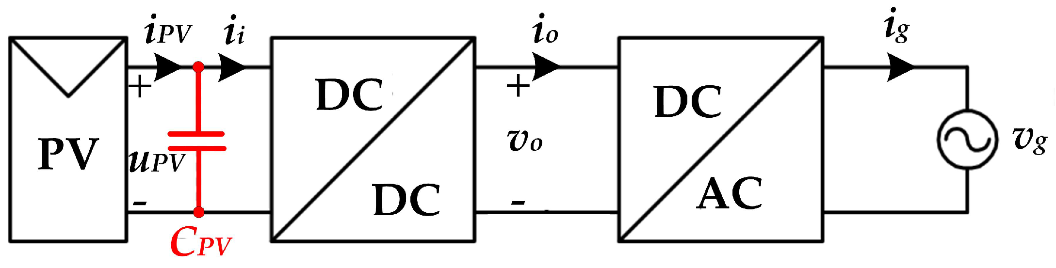
Figure 1 shows a block diagram of the complex of the DC–DC boost converter and grid-connected inverter, where the power decoupling capacitor is placed across the PV array. In this figure,
and
are the grid current and voltage, respectively, with the following equations:
where
and
are the peak of the grid current and voltage and
is the power factor angle. Disregarding the losses of the inverter and boost converter,
; thus:
Normally,
is set to zero (unity power factor operation) in the control of the grid-connected inverter [
18]. In this case, (
8) is simplified to
in (
9) consists of a ripple or AC component and a DC component,
. Since the impedance of the capacitive branch is low enough, it is reasonable to assume that the whole ripple component passes through
and generates a ripple voltage equal to
Therefore, the maximum amplitude of the ripple voltage is equal to
By combining (
6) and (
11), the minimum required capacitance to obtain the minimum permissible
is obtained as
Equation (
12) results in a relatively large capacitance that can be accomplished solely with electrolytic capacitors. On the other hand, the electrolytic capacitors are counted as a distinguishing factor in the lifetime of PV inverters.
It should be noted that the concept of single-stage power conversion was utilized in the formula presented in this section. This means that the DC-link capacitor was eliminated in the double-stage power conversion process. In other words, theoretically, there will be no need for the DC-link capacitor as long as the desired value of is accomplished by the proposed control structure.
3. Design of Energy Storage Elements for the PV Array under Study
Figure 2a shows the circuit of the DC–DC boost converter. In this section, the energy storage elements—
L and
C in
Figure 2a—are designed. For this purpose, the BP Solar BP4170B module was selected as the PV array, and the specifications were available from MATLAB models. The overall specifications are listed in
Table 1. In addition, for this case study,
,
and
. It should be mentioned that
were calculated based on the parameters in
Table 1 and according to the procedure explained in [
4]. According to
Table 1, the maximum achievable power was 170.88 W for each module. Therefore, a series connection of six modules was needed to obtain 1 kW of output power.
Table 2 summarizes the operating points required to design the energy storage elements and switching devices of the boost converter. Based on this table, the MPP voltage and current at a maximum irradiation of 1
were
and
, respectively. For the minimum irradiation, i.e.,
, these were
and
, respectively.
The input data for designing the energy storage elements were the input voltage,
, minimum input current,
, output voltage,
, permissible output voltage ripple,
, and switching frequency,
. The first two data were obtained according to the above-mentioned MPP characteristics. The maximum and minimum PV output voltages,
and
, were equal to
and
. The PV converter had to inject the power into the grid for the minimum irradiation [
4]. Thus, the minimum PV current at the lowest irradiation was
. It was assumed that the rms value of the single-phase grid voltage,
, changed in the range of
; then,
. In the control of a grid-connected inverter, the modulation index,
M, was set to near unity to minimize the harmonic content of the inverter output voltage and current [
19]. With these explanations and with
, the maximum DC-link voltage was calculated as equal to
. Hence,
was set equal to
. The allowable ripples on the DC–DC output voltage were considered as 1%. Finally, the converter switching frequency was 50 kHz.
Thus, all of the information required to design the energy storage elements is ready. The minimum inductance for meeting the continuous current mode (CCM) for the minimum irradiation level was calculated as equal to 3.3 mH. The output capacitance for meeting the maximum 1% of output voltage oscillations was obtained as equal to 16.8
(the complete design process based on the input data is explained in [
20] and is not repeated here for the sake of brevity). Then, the power decoupling capacitance had to be selected based on (
12). For this purpose, based on
Table 1, the maximum allowed ripple at the output of six series-connected PV modules was equal to 25.65 V, considering
. Hence, based on (
12), the minimum required power decoupling capacitance was calculated as nearly equal to 300
. Obviously, a 220 V, 300
capacitor is available as an electrolytic one, which, as explained earlier, reduces the reliability and lifetime of the PV structure. In the following part of this paper, a novel method for controlling the DC–DC boost converter is proposed with a remarkable reduction of the size of the power decoupling capacitor. Thus, the application of film capacitors is possible.
4. Transfer Functions and Current Mode Control in a PV-Connected DC–DC Boost Converter
Two general control methods are proposed in the literature for DC–DC boost converters [
4,
20]: voltage mode control (VMC) and current control mode (CMC). In VMC, also known as duty-cycle control, the purpose is to control the output voltage,
, and it consists of a single loop that directly adjusts the duty cycle to respond to variations in the output voltage. On the other hand, CMC consists of two loops: one internal current control loop and one external voltage control loop [
21]. The first one controls either the inductor peak (PCMC) or the average current (ACMC). A converter with CMC exhibits a proper dynamic response to input and output disturbances [
14].
In this paper, ACMC is utilized to control the output current of the PV array. Contrary to previous works, a single current control loop is adopted. Therefore, it is necessary to design the control structure according to the duty-cycle-to-inductor current transfer function, i.e., . An integral single-lead controller (ISLC) and a PI controller are utilized to compensate for the error between the reference and feedback currents of the inductor. In addition, it is shown that the transfer function exhibits a low amplitude at the SOFC and, therefore, reduces the amplitude of pulsations across the PV array. This is particularly beneficial in terms of using lower power decoupling capacitance.
4.1. Transfer Function of the DC–DC Boost Converter
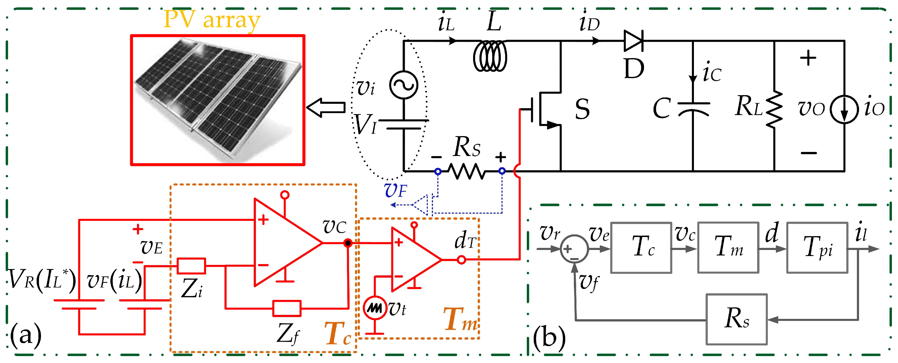
The aim is to control the inductor’s average current through the control circuit, as shown in
Figure 2a. An analog implementation of the control structure is presented due to its availability on integrated circuits (ICs), such as the TL494. This IC integrates all of the functions required by a PWM circuit with various applications, such as those in personal computers, switching-mode power supplies, PV AC modules, etc. [
22]. It is worth mentioning that the digital implementation of the control structure is also possible according to the presented transfer functions. According to
Figure 2a, a measuring resistance,
, was used to apply the circuit’s current to the controller. The switch’s duty cycle,
d, was generated through a comparison between the control voltage,
, and the reference in the modulator with the transfer function of
. By applying this duty cycle to the switch, the inductor current,
, was set to the reference value,
. In [
20], the linearized small-signal model of a DC–DC boost converter was presented by considering the effect of parasitic resistances of passive elements, diodes, and transistors. Through this model, the input-to-output transfer function in the Laplace domain was extracted with the following final equation [
20]:
in which
s is the Laplace operator and
and
d are small-signal variations in the inductor current and duty cycle, respectively. The amplitude of
at zero frequency is equal to
In this equation,
, with
being the nominal duty cycle, switch drain–source resistance, diode conducting resistance, and inductor resistance, respectively. In addition, the angular undamped natural frequency,
, and the damping ratio,
, are equal to
The quality factor is equal to
The transfer function
is generally a second-order low-pass filter with one zero,
, at the left-hand plane (LHP) and two poles,
and
, at the LHP:
With the parameters listed in
Table 3, the values of
, and
were calculated and are listed in
Table 4 for the designed DC–DC boost converter connected to the mentioned PV array. It should be mentioned that
and
were set equal to the average values of the PV output voltage and duty cycle, respectively.
4.2. Transfer Function of the Average Current Mode Controller
The loop gain of the block diagram shown in
Figure 2b is equal to
, with
and
being the pulse-width modulator and controller transfer functions, respectively. The pulse-width modulator is a sawtooth waveform changing linearly between 0 and
in a switching period of
. In other words, the slope of this change is equal to
. The control-voltage-to-duty-cycle transfer function in the small-signal domain,
, is as follows:
On the other hand, two controllers with a transfer function of
[
20] were considered for the implementation. One was an integral single-lead controller (ISLC), and the other was a PI controller, as described in the following.
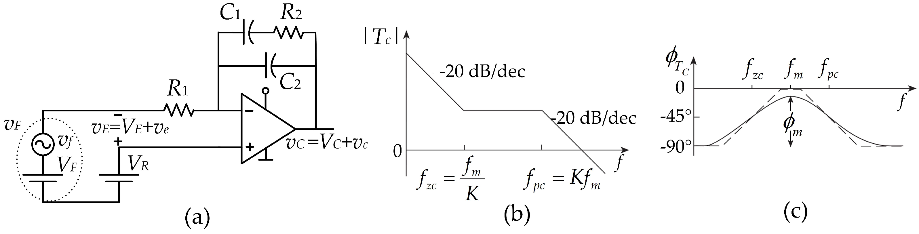
4.3. Integral Single-Lead Controller (ISLC)
The circuit diagram of an ISLC is shown in
Figure 3. This controller has a pole at the origin and a zero–pole pair. The pole at the origin makes the integral part and the zero–pole pair makes the lead part of the controller. The transfer function of the ISLC is obtained as in [
20].
Replacing
in (
18), the frequency response of the ISLC is obtained as
.
By taking the derivatives of the expression within the parentheses in the equation of
and setting them to zero, the frequency at which the phase-shift of
is at its maximum is acquired as
Substituting (
21) into (
20) yields,
The ideal (approximate) Bode plots for
are shown in
Figure 3b. According to this figure and (
22), the maximum phase shift, which is also known as the phase boost (shown in
Figure 3b by
), is
Figure 3.
ISLC, (
a) analog implementation, (
b) amplitude, and (
c) phase of ideal Bode plots [
20].
Figure 3.
ISLC, (
a) analog implementation, (
b) amplitude, and (
c) phase of ideal Bode plots [
20].
4.4. Proportional–Integral (PI) Controller
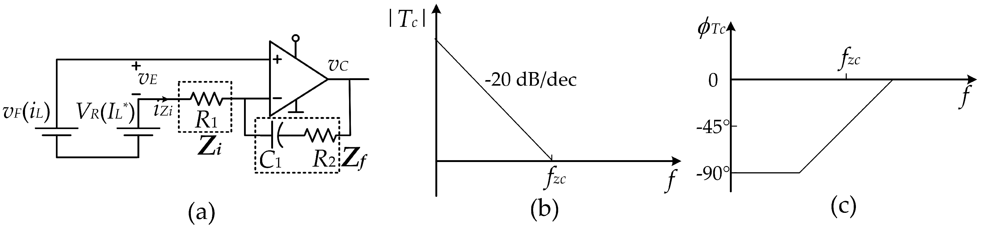
The reason for introducing this controller along with the ISLC is its simple implementation, for example, on the TL494. The analog implementation of the proposed PI controller is shown in
Figure 4a. The current
in
Figure 4a is calculated with the following equation:
By rearranging the above equation based on the control voltage,
,
According to the above equation, the small-signal control voltage, i.e.,
, is calculated as follows:
According to the relation of
, which are the small-signal portions of the error and feedback signals, respectively, (
26) turns into
Based on
Figure 4a, by putting
and
into (
28), the following transfer function is obtained:
By replacing
in the above equation, the transfer function in the frequency domain is obtained:
with the amplitude and phase of
The ideal Bode plots of the PI controller are shown in
Figure 4b,c. According to this figure, the maximum decrease in the phase (phase boost of the controller) is
4.5. Designing the ISLC
In this section, the ISLC is designed so that the phase margin of the open-loop transfer function,
, is equal to 60 degrees. The parameters mentioned in
Table 1,
Table 2,
Table 3 and
Table 4 are considered for the connection of the DC–DC converter to the PV array. For the starting point and according to the design recommendations made in [
23], the gain crossover frequency (GCF) was selected as equal to one-sixth of the switching frequency. Then, according to (
13) and (
17), the phase angle of the open-loop transfer function was calculated at the GCF while excluding the effect of the compensating transfer function (controller), i.e.,
with
. Thus, the required phase boost to have the necessary phase margin (
) was
This phase boost should be provided by the controller. Using (
22) and (
33),
Then,
K can be defined according to (
23), and, consequently, the angular frequencies of the controller pole and zero,
and
, are obtained based on (
19). On the other hand, the amplitude of the open-loop transfer function at GCF is unity, which means that
The above process was applied for the design of the ISLC with the parameters in
Table 3 and
Table 4. The designed parameters are shown in
Table 5. The Bode plots of the controller and open-loop transfer function are shown in
Figure 5a,b, respectively. A phase margin of 60 degrees was observed at the GCF, as shown in
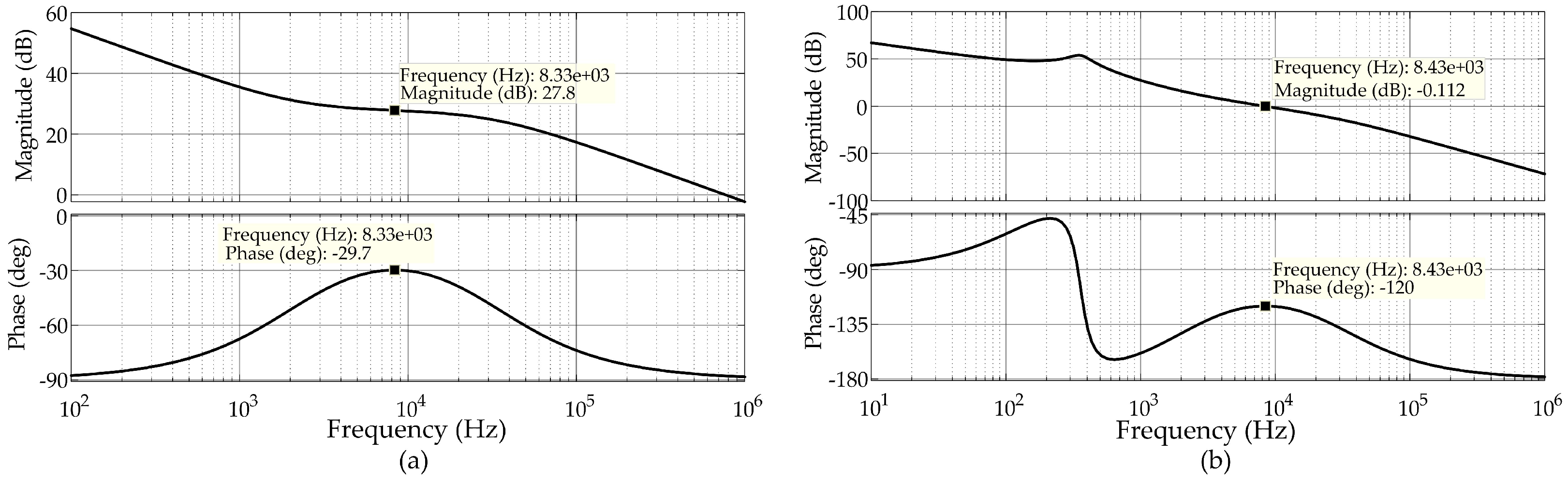
Figure 5b. However, with a GCF equal to 8.3 kHz, the phase margin was remarkably reduced at around 600 Hz. Hence, the disturbances at these frequencies could drive the controller into instability.
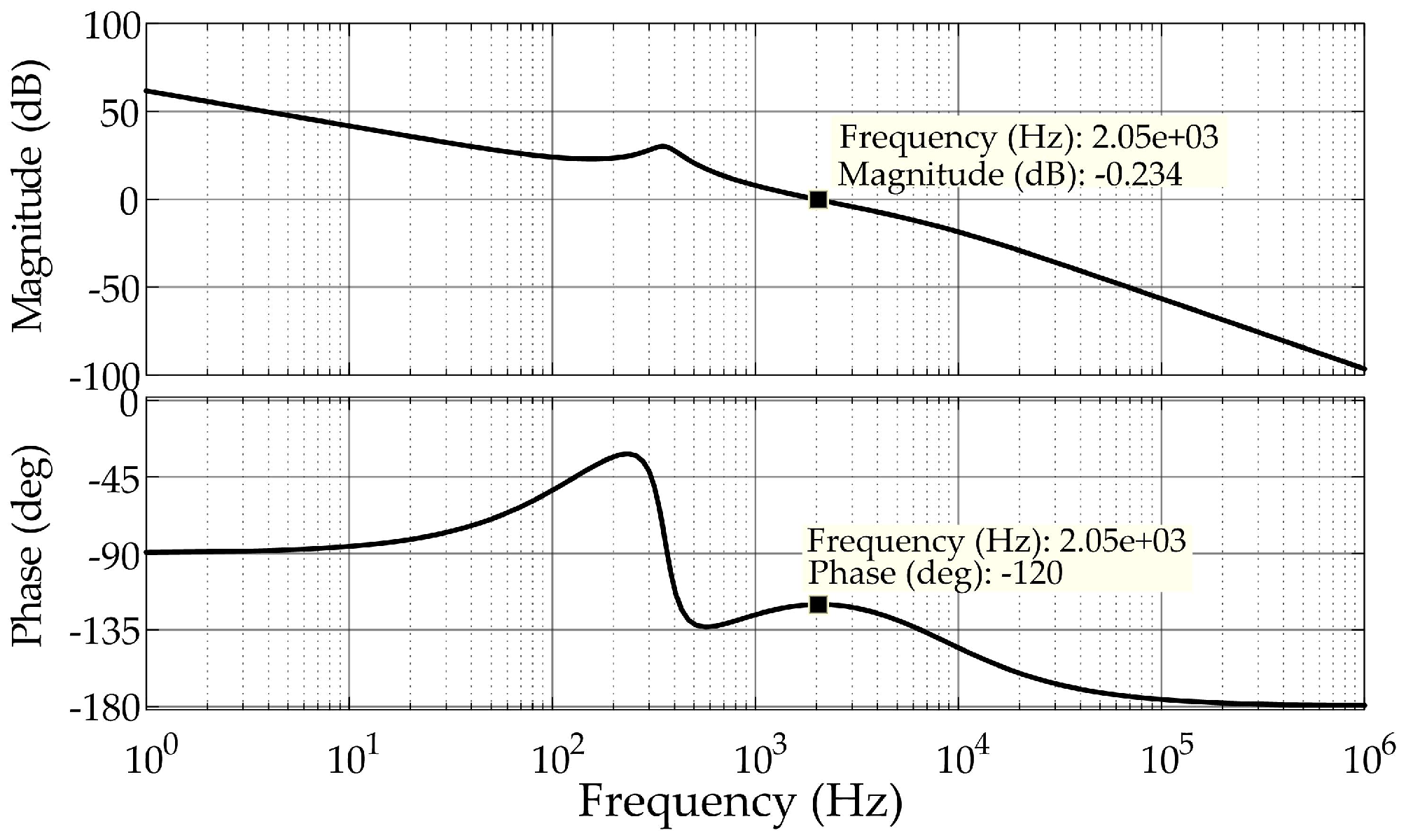
Table 6 lists the controller’s parameters for a GCF equal to 2 kHz. The Bode plot was redrawn for this crossover frequency, as shown in
Figure 6, where the required phase margin was observed in the intended frequency range. However, the decrease in the GCF increased the penetration of the SOFC into the input, and a trade-off had to be made for the selection of the GCF. This issue will be discussed in the next section.
4.6. Designing the PI Controller
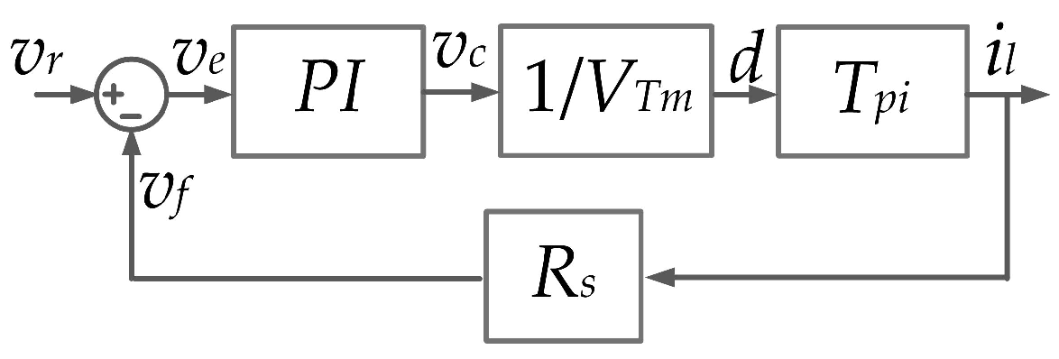
Similarly, the GCF was set to 2 kHz for the PI controller. A block diagram representation of the ACMC in a boost converter with a PI controller is shown in
Figure 7, in which the closed-loop transfer function for this controller,
, is obtained as
By defining the phase angle at the GCF according to (
13) and considering a phase margin of 60 degrees, the required phase boost of
was calculated based on (
34). Then, the angular frequency of the PI controller zero was obtained based on (
32). Furthermore,
K in (
18) was recognized, as it was known that the amplitude of the controller’s transfer function should be the inverse of the amplitude of
at the GCF:
Table 7 lists the PI controller parameters for the designed boost controller with a GCF equal to 2 kHz. In addition, the Bode plots of the controller and open-loop transfer functions are drawn in
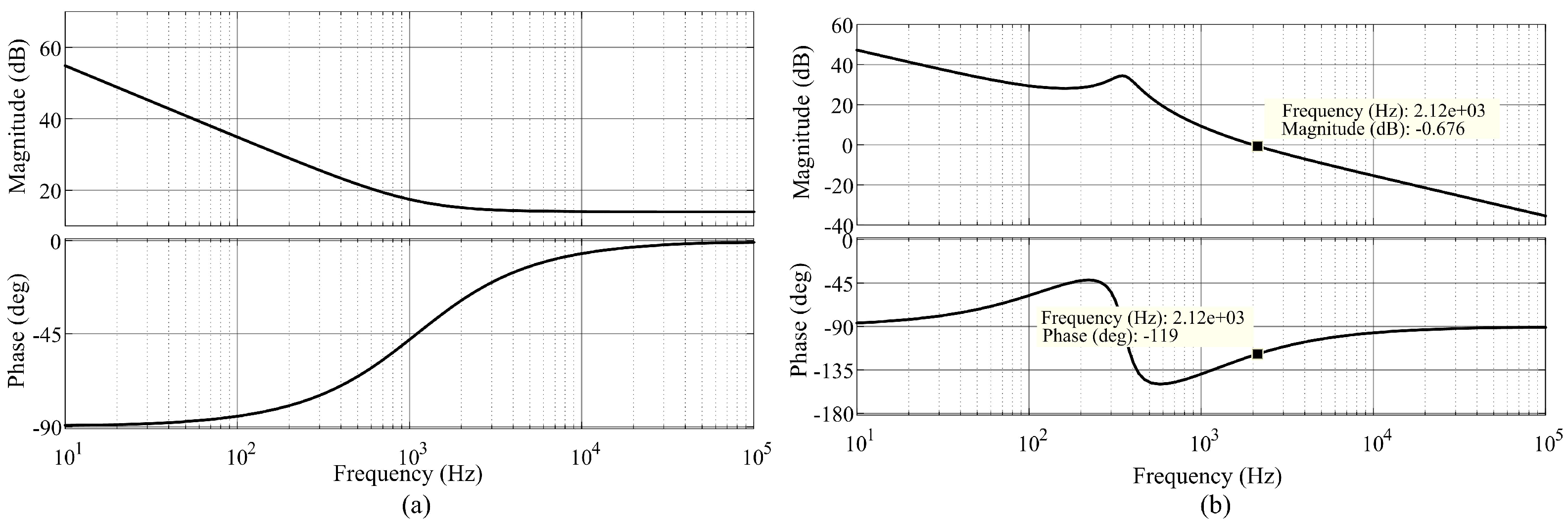
Figure 8a,b, respectively. According to
Figure 8b, a phase margin of 60 degrees was observed at GCF = 2 kHz. However, the phase margin was reduced to 30 degrees at the frequency of 500 Hz, which could influence the converter’s stability under low-frequency disturbances.
Figure 7.
Block diagram representation of the ACMC’s closed-loop control with a PI controller.
Figure 7.
Block diagram representation of the ACMC’s closed-loop control with a PI controller.
5. Design of a Power Decoupling Capacitor Based on the Allowable Utilization Factor
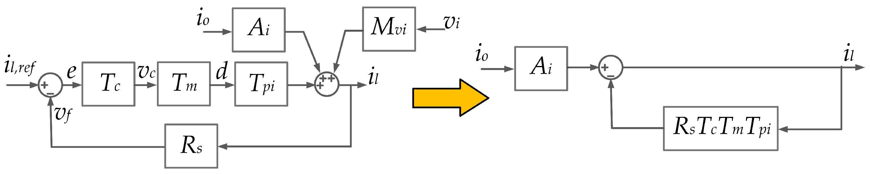
The effects of the studied controllers on the penetration of the SOFC into the input are investigated in this section. For this purpose, first, the open-loop transfer function from the output disturbance current,
, to the inductor’s small-signal current,
(
, as shown in
Figure 2a), was obtained according to the block diagram shown in
Figure 9, where the factors contributing to the small-signal variations in the inductor current were
, and
d. In [
20], a procedure for finding
was presented based on a small-signal model of the circuit, and the final equation is mentioned here for the sake of brevity:
Then, the closed-loop transfer function was obtained based on
Figure 9. Setting
and
equal to zero, the transfer function was obtained as
Figure 9.
Small-signal model of the boost converter in the ACMC of the inductor current.
Figure 9.
Small-signal model of the boost converter in the ACMC of the inductor current.
Replacing (
18) in (
40), for the ISLC,
is
where,
On the other hand, replacing (
37) in (
41), for the PI controller,
is
where
Consequently, the SOFC for the two introduced controllers at the input of the boost converter is
. The voltage ripple due to this current ripple is calculated based on (
10). The Bode plots of (
41) and (
43) are shown in
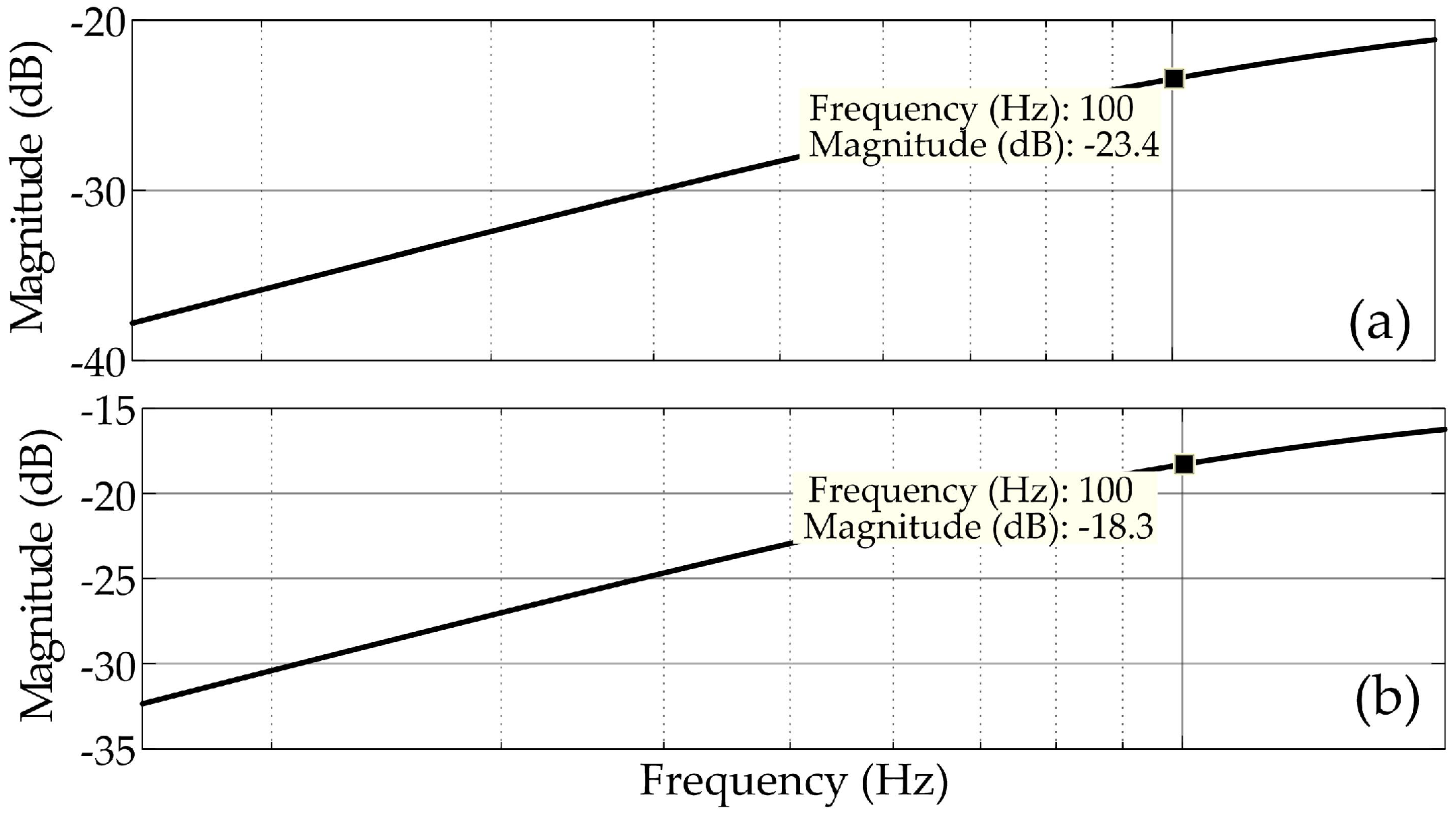
Figure 10 under the same gain crossover frequency.
Figure 10 reveals that the PI controller has better SOFC rejection capabilities compared to those of the ISLC at the cost of a lower phase margin under low-frequency disturbances. The amplitude of the SFOC in the input inductor current is 6.76% of that in the output current for the PI controller, while it is 12.16% for the ISLC.
In summary, the design procedure is as follows. First, (
6) is used to calculate the allowable voltage ripple of the PV array based on the minimum allowable utilization factor,
. Second, considering a capacitance that could be implemented by the film capacitors,
is obtained based on (
8). Third, the value of
, which is the SOFC of the DC-link current, is computed while assuming the equal input and output powers of the inverter:
with
being the DC-link voltage. Finally, the GCF is computed so that
.
For the designed PV system, the maximum allowable voltage is calculated as equal to 25.65 V in order to have . Therefore, the current ripple of a 40 film power decoupling capacitor is equal to 0.645 A. On the other hand, the maximum current ripple at the output of the boost converter, , is 6.43 A for the power of 1 kW and V. In other words, the amplitude of at an SOFC of 100 Hz must be equal to . With the procedure explained for the PI controller, a gain crossover frequency of 2 kHz is adequate to observe the permissible voltage ripple with a 40 capacitor.
The complex of the PV array and the DC–DC boost converter were implemented in MATLAB/SIMULINK with the designed circuit elements to verify the efficacy of the proposed design procedure. For the simulation studies, the voltage and current of the PV array were controlled at its MPP for different irradiation levels with the incremental conductance (IC) method. The temperature of the PV panels was considered to be equal to
in the simulations. In addition, a fixed voltage source equal to 350 V was placed at the output to replace the single-phase grid-connected inverter.
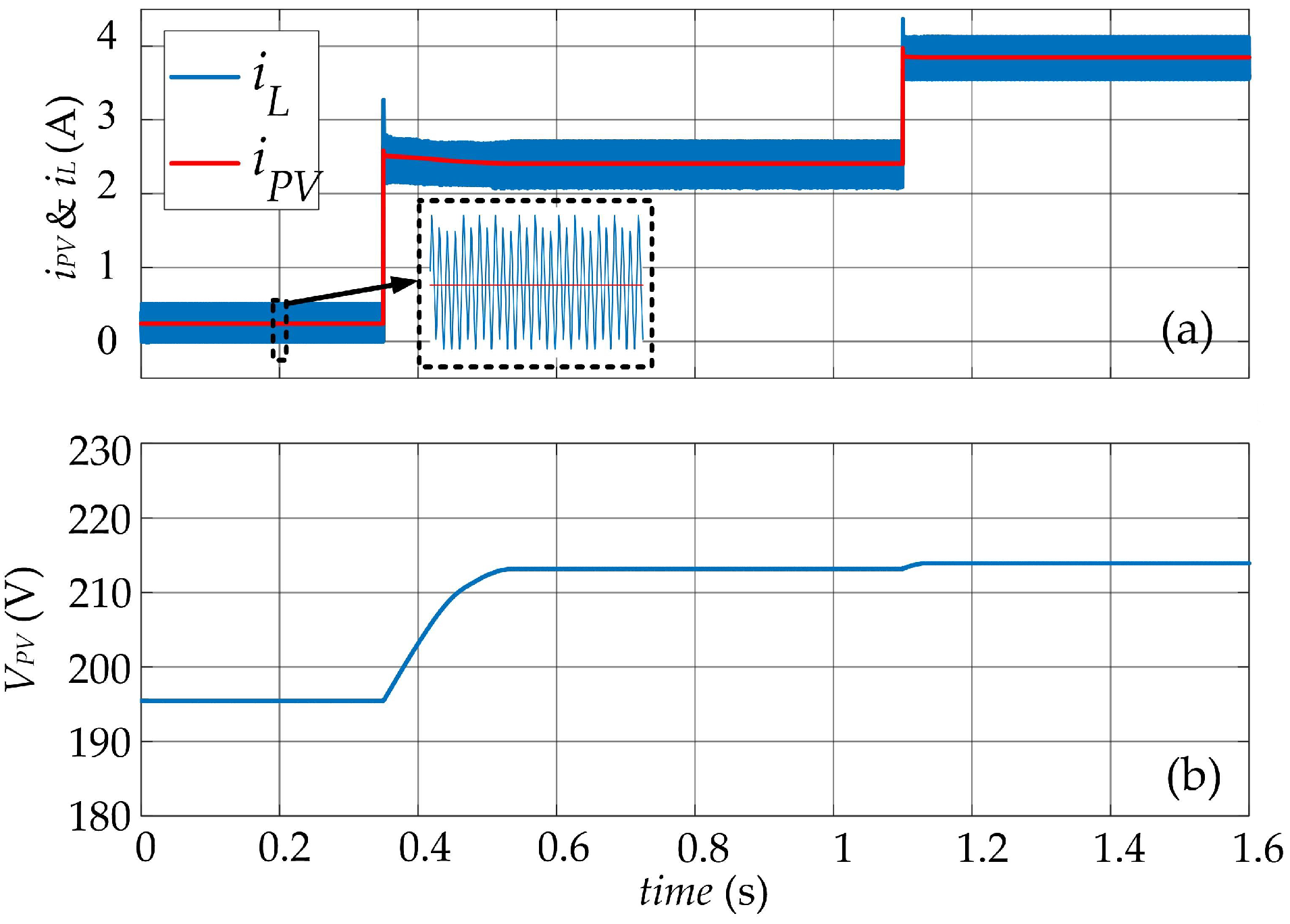
Figure 11 shows the simulation results of the inductor current for three irradiation levels of 50, 500, and 800
. According to this figure, the inductor current could perfectly follow the reference value (that is, the output of the IC algorithm), which is indicative of the proper design of controllers (the results for the PI controller and ISLC were the same).
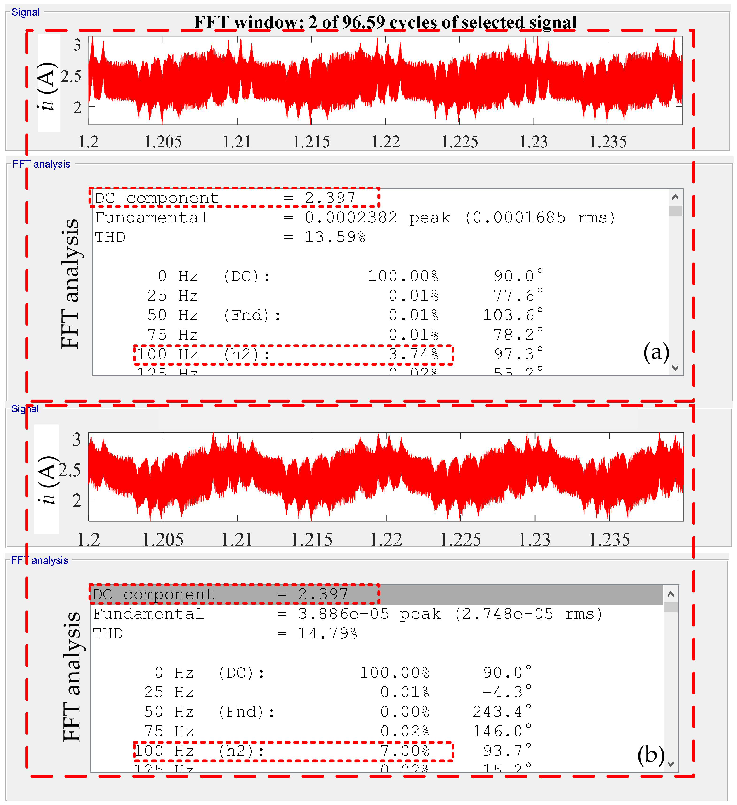
In the next step, a current source was connected in parallel with the output of the DC–DC boost converter to represent the SFOC disturbance.
Figure 12 shows a Fourier analysis of the inductor current with the ISLC and PI controller. The amplitude of the SFOC in the inductor current was lower for the PI controller. Furthermore, with the designed GCF, the amplitude of the input SOFC was, at most, 7% in the case of the ISLC and the maximum irradiation level. This was below the 10% considered for the amplitude of
, which created the maximum permissible voltage ripple of 25.65 V in the presence of a 40
power decoupling capacitance.
The propagation of the SOFC could be decreased further by selecting a higher GCF.
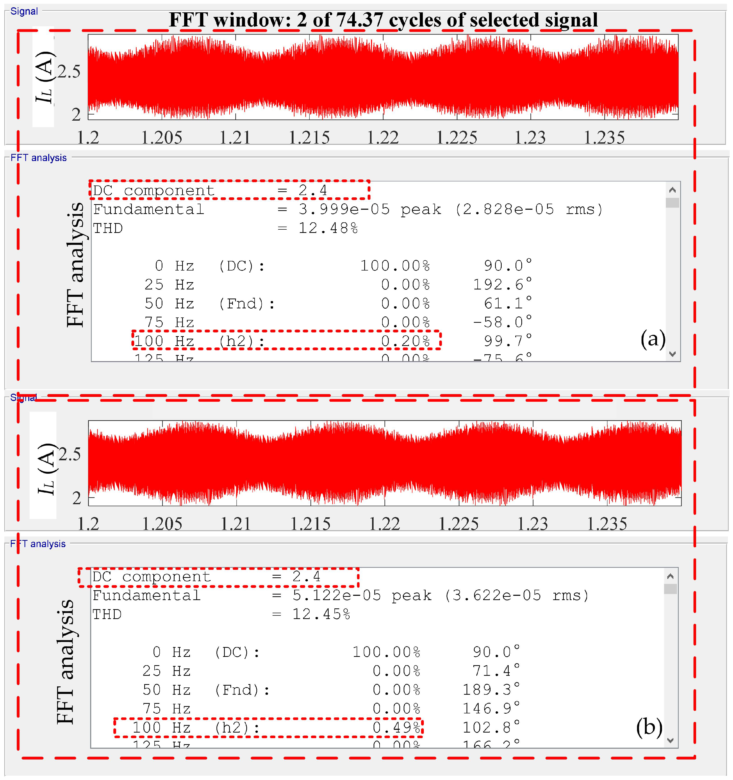
Figure 13 shows the simulation results of the inductor current for GCF = 8.33 kHz. This figure indicates the drastic shrink in the input SOFC compared to the case when the GCF was equal to 2 kHz (0.2% versus 3.74% for the PI controller). However, attention should be paid to the reduced phase margin under low-frequency disturbances.
6. Conclusions
The propagation of second-order frequency components (SFOCs) into an input PV array aggravates the energy harvesting efficiency in single-phase grid-connected inverters. Auxiliary circuits are added or modifications in the control loops are made to avoid the use of bulky electrolytic capacitors. This paper proposes the use of average current mode control (ACMC) to impose a high impedance toward SOFCs. The transfer function from the output oscillatory current to the input inductor current, , is extracted when two types of controllers are utilized, i.e., an integral single-lead controller (ISLC) and a proportional–integral (PI) controller. These controllers must be designed for the specific case of PV-grid-connected inverters, since the transfer function depends on the gain crossover frequency (GCF), zeros, and poles of controllers and their gains, which all depend on the switch’s duty cycle and, consequently, the operating point of the PV array. It is shown in this paper that the GCF greatly affects the amplitude of . Higher GCFs are advantageous in terms of a drastic reduction in the input current and voltage ripples, but at the cost of a phase margin reduction in the low-frequency range. This paper introduced a design procedure based on the allowable utilization factor of a PV array (maximum allowable voltage ripple at the output of the PV array). Then, the GCF was selected based on the amplitude of and the available film capacitor. This showed that the required power decoupling capacitance was significantly reduced ( compared to ) by applying the presented design procedure.


