Article

High-Frequency Oscillation of the Active-Bridge-Transformer-Based DC/DC Converter

1
Department of Electrical Engineering, Tsinghua University, Beijing 100084, China
2
Key Laboratory of Military Special Power Supply, Army Engineering University of PLA, Chongqing 400035, China
*
Author to whom correspondence should be addressed.
Energies 2022, 15(9), 3311; https://doi.org/10.3390/en15093311
Submission received: 5 April 2022 / Revised: 24 April 2022 / Accepted: 27 April 2022 / Published: 2 May 2022
(This article belongs to the Topic Power Converters)

Abstract

:
The dual-active-bridge converter (DAB) has attracted tremendous attention in recent years. However, its EMI issues, especially the high-frequency oscillation (HFO) induced by the dv/dt and parasitic elements of the transformer, are significant challenges. The multi-active-bridge converter (MAB) based on the multi-winding transformer also faces similar problems, which are even more complicated. This article investigates the HFO of active-bridge-transformer-based DC/DC converters including DAB and MAB. Firstly, the general HFO model is studied using the analysis of the AC equivalent circuit considering the asymmetrical parameters. Ignoring the AC resistance in the circuit, the high-order model of the voltage oscillation could be reduced to a second-order system. Based on the simplified model, the oscillation voltage generated by an active bridge is analyzed in the time domain. Then, a universal active voltage-oscillation-suppression method-selected harmonic-elimination phase-shift (SHE PS) modulation method is proposed. The impacts of the system parameters on the method are also revealed. The experimental results show the excellent performance of the proposed active suppression method, with voltage spike amplitude (VSA) reductions of 92.1% and 77.8% for the DAB and MAB prototypes, respectively.

1. Introduction

The dual-active bridge (DAB) converter has continued to be a hot topic in both academia and industry in recent years, due to its properties of bidirectional power flow, high power density, soft switching, and inherent galvanic isolation [1,2]. The multi-active bridge converter (MAB), regarded as the natural expansion of DAB, could provide multi-ports to integrate multiple DC voltage domains, making it a competitive candidate in many applications such as power electronic transformers (PETs), electric aircrafts and all-electric ships, and energy routers for smart homes [3,4]. To make the MAB more flexible and scalable, the modular multi-active bridge (MMAB) converter has been proposed, where one multi-winding transformer is replaced by several dependent two-winding transformers.
With the increasing switching speed, the high-frequency oscillation (HFO), which is excited by the output voltage of the active bridge and the transformer stray parameters in the DAB, has raised concern. Recently, wideband gap (WBG) devices have been widely used in DAB converters and other H-bridge-based converters [5,6,7,8,9], which could increase the system’s efficiency. With the WBG switching devices and the nanocrystalline alloys utilized, the HFO at the ac side of the DAB converter represents an urgent problem that needs to be solved [8]. The HFO in the DAB could increase the voltage stress of the transformer, induce EMI and common mode noise, and distort the waveforms [8]. Additionally, it may increase the high-frequency losses, decreasing the system’s efficiency. The HFO of the MAB converter has not been reported in the existing literature, but can be naturally predicted. Figure 1 shows a three-winding MAB, which is also called a triple-active bridge (TAB) converter, and the waveforms. The dv/dt is 3 kV/us and obvious voltage HFO exists with the high frequency near 1 MHz.
To modify the dv/dt [8,9] to suppress the voltage spike amplitude (VSA) using the extra parallel capacitor involves deceasing the switching speed and adding extra hardware components. The optimization of the inductor and transformer stray capacitors [10,11] will increase the complexity of the design procedure. The split inductance tunning between the HV and LV side [12] is often a special case without generality, which may lose effectiveness for multi-port converters. The active selective harmonic-elimination general phase-shift PWM method is introduced to suppress the HFO of the AC-link in MMAB [13], which has the potential to suppress the HFO of the transformer of the DAB and MAB, but has not been derived or verified. On the other hand, the branches of the DAB [10] and MMAB converters [13] are symmetrical with 1:1 transformer turn ratios and the same phase-shift inductors.
The HFO mechanism of active-bridge-transformer-based DC/DC converters, including DABs and MABs, is investigated in this article. The converters with asymmetrical inductances are considered for the general case study. On top of that, the universal SHE PS modulation method to suppress the voltage oscillation is proposed and the impacts of the system parameters on the method are studied. Finally, the effectiveness of the proposed voltage suppression method is verified by the experimental results of a DAB and MAB prototype.

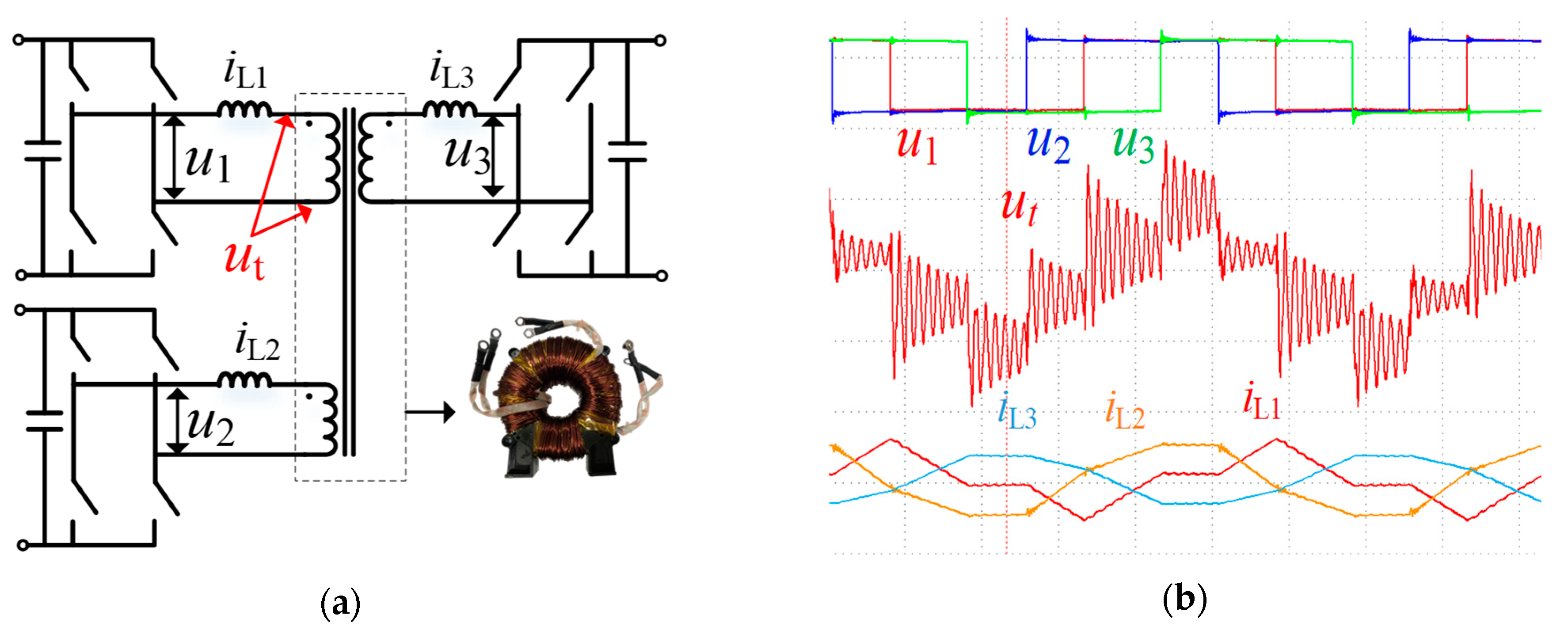
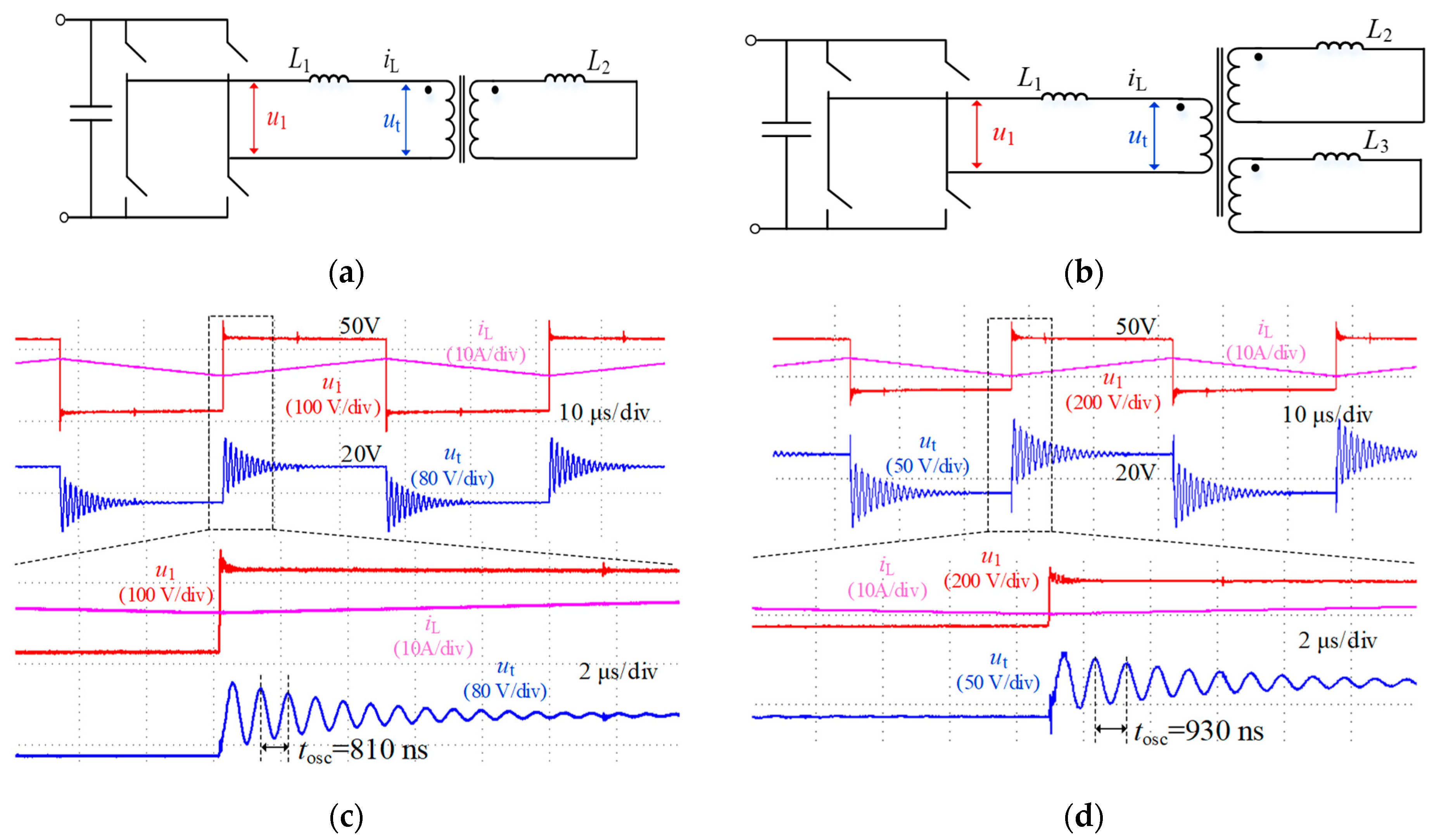
2. High-Frequency Oscillation of the Active-Bridge-Based DC/DC Converter

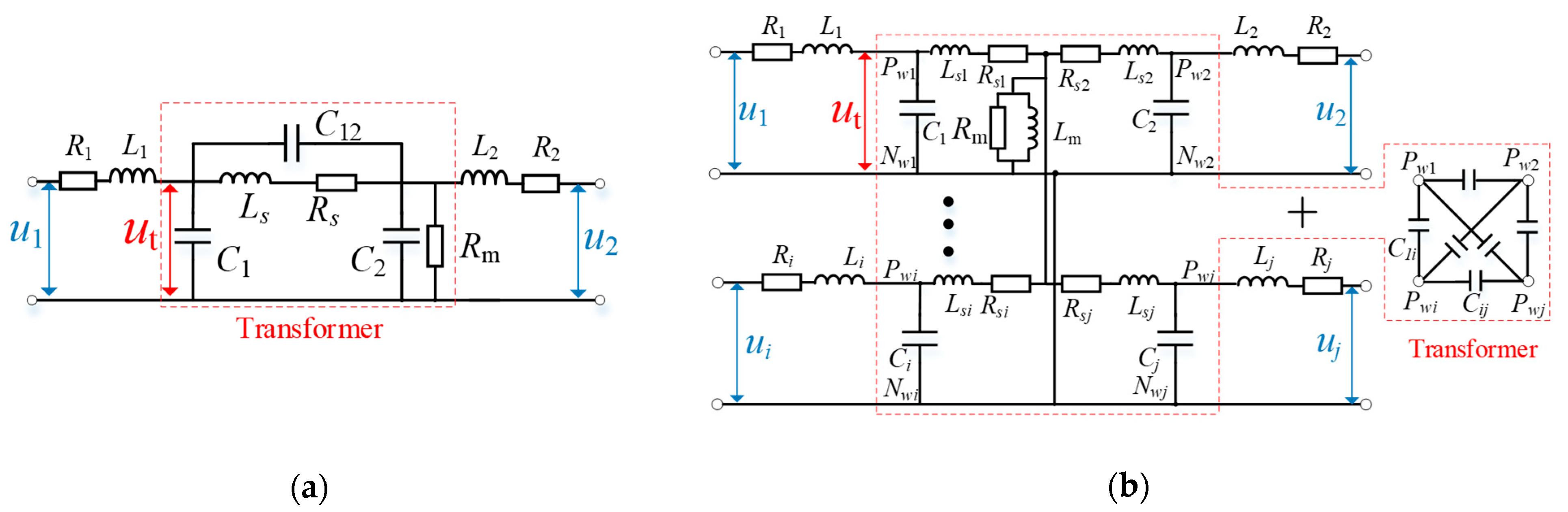
2.1. Equivalent Circuit of the Transformers

The active bridge with the transformer is the core unit in active-bridge-transformer-based converters. Stray capacitances are regarded as the major factor causing the HFO phenomenon. A classical π-shaped network with three capacitors [6,7,9] is used to model the HFT. The high-frequency (HF) equivalent circuits of the DAB and MAB converters considering the stray parameters of the transformers are shown in Figure 2. The parameters are referred to the primary side. The symbols are defined as follows: ui is the AC voltage of the active bridge i, Li and Ri are the inductance and the equivalent resistance of the phase-shift inductor i. Ls and Rs are the leakage inductor and the equivalent winding resistance of the transformer, Lm is magnetizing inductance, and Rm is the magnetizing resistor. C1 and C2 are self-capacitances of the primary side and the secondary side, which is referred to the primary side, respectively. C12 is the mutual capacitance between the two windings. Similarly, the extended π-shaped network could be utilized to model the circuit for the multi-winding transformer [14]. Ci is the self-capacitance of the windings and Cij is the mutual capacitance between the two windings i and j.
As shown in Figure 2, the HF voltages of the transformer ut of the DAB and MAB are the superposition of the responses of each excitation voltage, which can be regarded as the multi-input single-output (MISO) impedance model.

2.2. General HFO Model with the Asymmetrical Branch Parameters
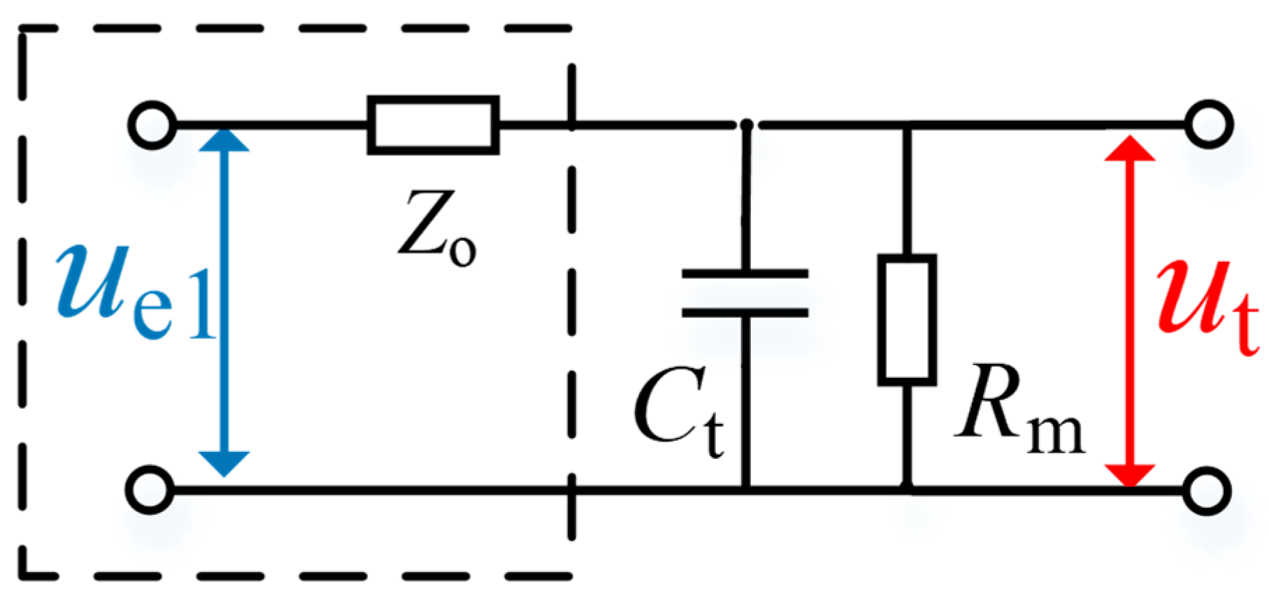
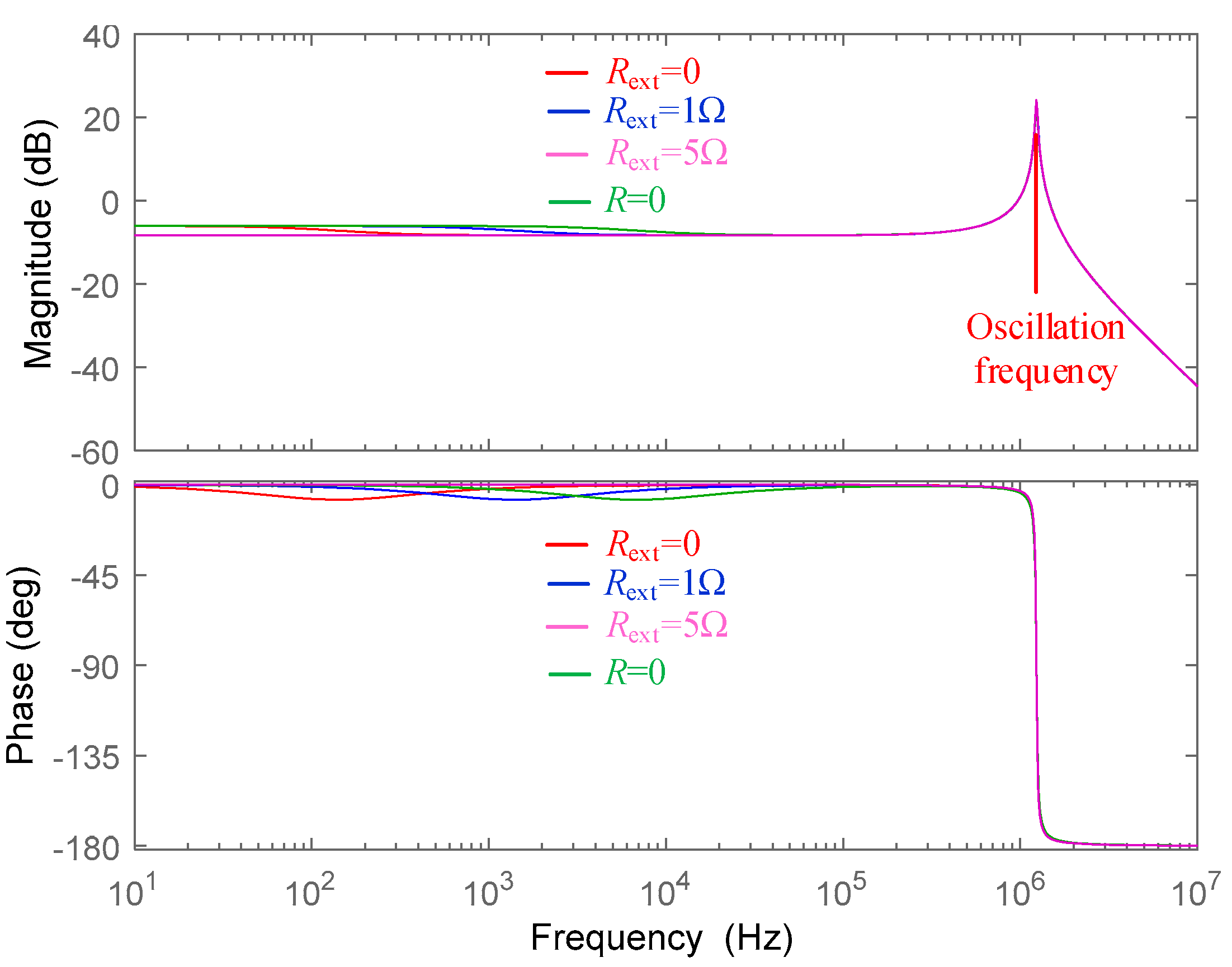
Assuming Ls << Lm and Ls is small compared with phase-shift inductance L, the AC equivalent of the DAB can be simplified to be an equivalent model [8]. Considering the general case for the DAB and MAB converters, one excitation voltage u1 was taken into consideration while the other active bridges short-circuited. Then, we could obtain the single-input single-output (SISO) impedance model shown in Figure 3, where ue1 is the equivalent excitation voltage, Zo is the internal resistance, and Ct is the equivalent capacitance.
The variables in the two-port network in Figure 3 can be derived using Thevenin’s theorem:
u e 1 ( s ) = Z 2 | | Z 3 | | | | | Z n Z 1 + Z 2 | | Z 3 | | | | | Z n u 1 ( s ) ,   Z o = Z 1 | | Z 2 | | Z 3 | | | | | Z N
Z i = R i + L i s ,   C t = i = 1 N C s i
The voltage transfer function of Gh(s) = ut(s)/u1(s) for the DAB circuit in Figure 2b was derived by:
G h ( s ) = u t ( s ) u 1 ( s ) = R m ( L 2 s + R 2 ) L 1 L 2 R m C t s 3 + [ ( L 2 R 1 + L 1 R 2 ) R m C t + L 1 L 2 ] s 2 + [ R m C t R 1 R 2 + L 1 R 2 + L 2 R 1 + R m ( L 1 + L 2 ) ] s + R 1 R 2 + R m R 1 + R m R 2
The transfer function (4) is a third control system. For MAB, with the increasing branches, the order of the transfer would be increased, making it difficult to calculate the analytical solution. Thus, it was necessary to simplify the model.
The impedance of the inductor was much larger compared with the AC resistance including the wire, inductor and transformer resistance at the oscillation frequency. It was reasonable to reduce the system order by ignoring the resistance. The external resistors Rext were inserted into the AC loop of the DAB converter to investigate the effect of AC resistance on the HFO, as shown in Figure 4.
The magnitude and phase of the voltage transfer function (3) are illustrated in Figure 5. R = 0 means R1 = R2 = 0 and no external resistors were inserted to the AC loop. It can be seen that the AC resistance only affected the magnitude at low frequency, while the magnitude and phase were irrelevant to the AC resistance. Figure 6 shows the experimental waveforms of a DAB converter using different external AC resistors. Both the oscillation frequency and amplitude were the same with different AC resistances.
Then, ignoring the AC resistance of the loop, the transfer function could be simplified from the third-order control system to a standard second-order control system, as shown in Equation (4). The steady state value of the ut considering both u1 and u2 was calculated as follows in (5).
G hS ( s ) = u t ( s ) u 1 ( s ) = 1 L 1 C t 1 s 2 + 1 R m C t s + L 1 + L 2 L 1 L 2 C t
u t , S = L 2 L 1 + L 2 u 1 + L 1 L 1 + L 2 u 2
Thus, for MAB, the transfer function could be derived as (6):
G hS ( s ) = u t ( s ) u 1 ( s ) = 1 L 1 C t 1 s 2 + 1 R m C t s + L 1 + L 2 e L 1 L 2 e C t
where L2e is the equivalent inductance as L2e = L2 ||… || LN. The simplified transfer function (6) can be utilized to analyze the HFO of the DAB and MAB converters, generally.

3. Model Analysis

The transfer functions (4) and (6) were standard underdamped second-order control systems when the damping ratio met the inequality:
ξ = 1 2 R m C t L 1 L 2 C t L 1 + L 2 < 1
For a highly efficient HFT with little iron loss, the inequality (7) was easily met. When the excitation (i.e., the step change voltage) appeared, there was voltage oscillation, which gradually decayed. The natural frequency ωn and oscillation frequency ωOSC were calculated as follows:
ω n = L 1 + L 2 L 1 L 2 C t ,   ω OSC = 1 ξ 2 ω n
Furthermore, ignoring Rm, which yielded ξ = 0 and ωosc = ωn, ωosc could be derived as follows:
ω OSC = ω n = 1 / [ 1 / ( i = 1 N 1 / L i ) k = 1 N C s k ]
The result was symmetrical, which means the period of the oscillation induced by the excitation source at any port was the same. According to the rated transferred power of DAB, the splitting inductors should meet:
L 1 + L 2 = 2 L ph
Combing (9), the oscillation of DAB is written as:
{ ω OSC = 2 L p h / ( C 1 + C 2 ) / L 1 / ( 2 L ph L 1 ) ω OSC , min = 1 / ( C 1 + C 2 ) L ph / 2
The minimum oscillation frequency ωosc,min is achieved when L1 = L2 = Lph. Tuning the splitting inductances to move the oscillation frequency, which represents the pole point in (4), to the first zero cross point (ZCP) of the excitation voltage is the basic principle in [12].
The DAB and TAB prototypes were setup to test the model. The parameters are shown in Table 1.
Square wave u1 at the primary AC side was used as the excitation source while the secondary AC side short-circuited. It was easy to run the test with a small excitation amplitude of 50 V. Obvious oscillation appeared after the u1 step changed and decayed to zero with several cycles, as shown in Figure 7c. To substitute the parameters of the transformer and inductor into (5), we obtained ξ = 0.039, ωosc = 0.99ωn, and tosc = 810 ns. The theoretical oscillation period matched well with the test results.
The test circuit could be utilized to estimate the damping characteristics and to pre-obtain the oscillation frequency. For multiport converters, all the other branches should be short-circuited except the excitation port. Figure 7b,d show the test short circuit and the waveforms of the TAB converter, where branch 2 and 3 were short-circuited.

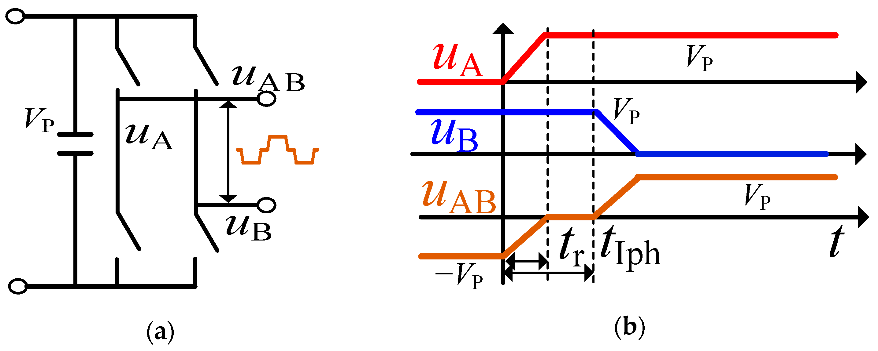
4. Active Suppression Method for the HFO

4.1. General Description of the Voltage Excitation

The excitation source of the active-bridge-transformer-based converter, generated by the active bridge, was the superposition of the two half bridges [15]. As shown in Figure 8, the phase voltages uA, uB and the output voltage uAB were modeled by segmental linear functions considering the inner phase shift and transient time as:
{ u A ( t ) = V P / ( t r ) [ t e ( t ) + ( t t r ) e ( t t r ) ]   ,   u B ( t ) = u A ( t t Iph ) u AB ( t ) = u A ( t ) u B ( t ) = u A ( t ) + u A ( t t Iph )
where VP is the DC bus voltage, uB lags behind uA with time tIph, and tr is the transient time.

4.2. Active SHE PS Suppression Method

To modify the inner phase-shift tIph, reducing the harmonics of the oscillation frequency is an effective way to suppress the oscillation, which is called the selective harmonic elimination phase-shift (SHE PS) modulation method. Combing (12) with the transfer function (4), ut,A, the high-frequency voltage which represents the zero-state response of uA, was derived as:
{ u t , A ( t ) = 0.5 k e k r ( t r / ( α 2 + β 2 ) + M e α t cos ( β t + θ 1 + θ 2 ) ) θ 1 = arctan ( α 2 β 2 ) / ( 2 α β ) ,   θ 2 = arctan ( sin ( β t r ) / ( 1 e α t r cos ( β t r ) ) k e = 1 / ( L 1 C t )   ,   k r = 2 V P / t r
where α and β are written as:
α = 1 2 R m C t ,   β = 1 2 4 ( L 1 + L 2 ) L 1 L 2 C t ( 1 R m C t ) 2
Thus, the zero-state response of ut,AB could be derived, combining (12) and (13) as:
{ u t , AB ( t ) = V 1 L 1 / ( L 1 + L 2 ) + M e α t f ( t Iph ) cos ( β t + θ 1 + θ 2 + θ 3 ) θ 3 = arctan ( e α t Iph sin ( β t Iph ) / ( 1 + e α t Iph cos ( β t Iph ) ) M = V P ( 1 e α t r cos ( β t r ) ) 2 + sin 2 ( β t r ) / ( L 1 L 2 C t t r ( α 2 + β 2 ) β / ( L 1 + L 2 ) )
M is constant. The amplitude f(tIph), which is a function of inner phase-shift tIph, was derived as:
f ( t Iph ) = ( 1 + e α t Iph cos ( β t Iph ) ) 2 + e 2 α t Iph sin 2 ( β t Iph )
The f(tIph) in Equation (16) could be derived as:
α t Iph 0   e α t 1     f ( t Iph ) 2 + 2 cos ( β t Iph )
Thus, the minimum of the VSA could nearly be achieved at the following condition:
β t Iph = π   ,   t Iph = π / β = 0.5 T osc
To substitute (18) into (16), the minimum fmin(tIph) and the corresponding VSA Amin were derived as:
f min ( t Iph ) = 1 e α π β   ,   A min ( t Iph ) = 1 2 k e k r M ( 1 e α π β )

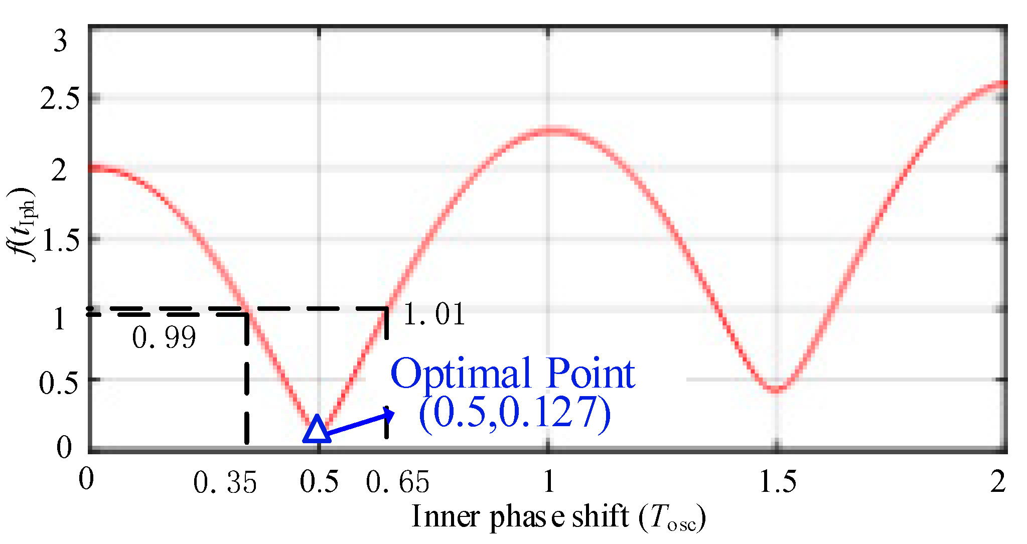
4.3. Impact of the System Parameters on the SHE PS Modulation Suppression Method

4.3.1. Inner Phase-Shift Accuracy

As seen in Equation (18), the SHE PS modulation utilizes the inner phase-shift, which equals half of the oscillation period to eliminate the HFO. When the frequency was high, the phase-shift accuracy should be considered due to the time resolution of the controller and the non-ideal factors of the circuit, i.e., different time delay of the driver signals.
Considering the f(tIph) with different inner phase-shifts, we drew the curve of oscillation amplitude vs. the inner phase-shift, as shown in Figure 9. The amplitude value decreased when the inner phase-shift was applied, and it reached its optimal point when tIph = 0.5Tosc. The VSA still fell to the half of the unsuppressed value when applying the inner phase-shift even with ±30% error, which verifies the robustness of the method in terms of inner-phase accuracy.

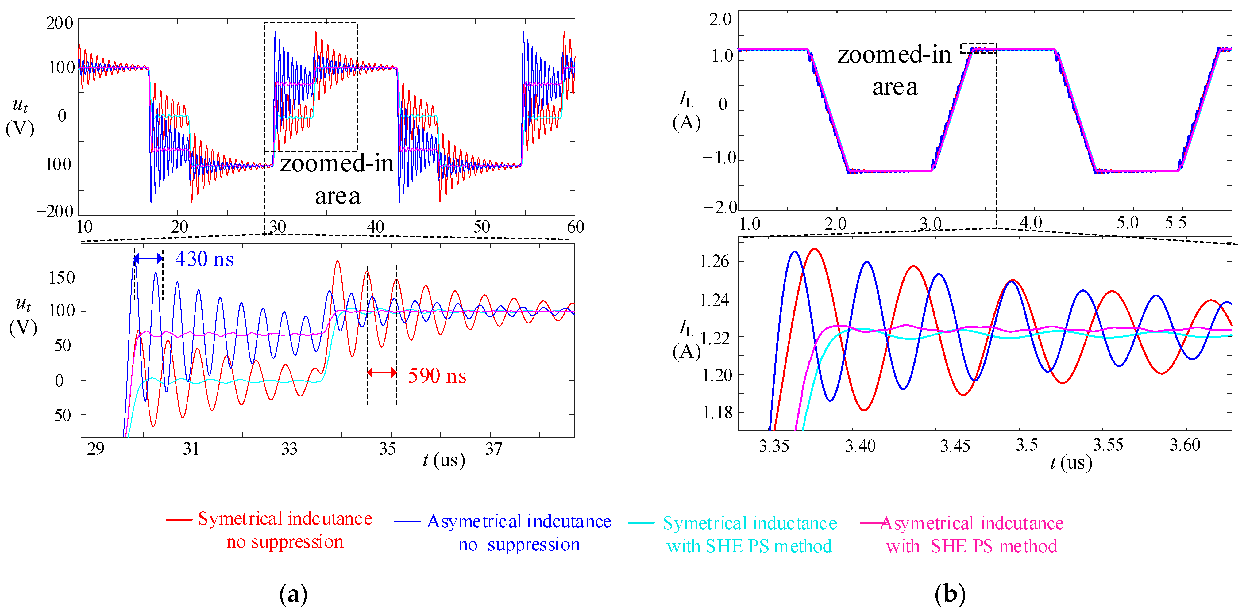
4.3.2. Asymmetrical Splitting Inductances

The oscillation frequency changed with the varying splitting inductances according to (11), which could be verified in the simulation results in Figure 10. Two cases of splitting inductances were considered: the symmetrical case with Lph1 = Lph2 = 160 μH, and the asymmetrical case with Lph1 = 50 μH, Lph2 = 274 μH. The simulated waveforms show that the voltage and current oscillations were immigrated to a negligible level for both the symmetrical and asymmetrical situations when the SHE PS modulation method was adopted.

4.4. Comparison with Other Suppression Methods

The proposed active method was from the perspective of the excitation source. The comparisons between the proposed method and the existing methods in the literature [8,9,10,11,12,13] are listed in Table 2.
The existing methods in [8,9,10,11,12] are passive methods. For [8,9], external capacitors were connected in parallel with the drain and source of the MOSFET to modify the dv/dt of the AC voltage of the bridges, which limited the switching speed of the devices. Additionally, the analytical model in [8] was based on the symmetrical parameters with the same two phase-shift inductors on the primary and secondary sides, respectively. On the contrary, the model in this article considered the asymmetrical parameters. In practice, the parameters for the MAB were not always symmetrical for the different branches.
The method in [11] optimizes the stray capacitance of the transformer by the optimal design of the transformer in the DAB converter, which is difficult. For the MAB with more windings, the design complexity was increased.
The different effects of the phase-shift inductors of the primary and secondary side on the impedance of the resonant tank were analyzed. The asymmetrical splitting inductances with the transformer turn ratio N1:N2  1 were utilized to suppress the oscillation by modifying the ZCP of the AC impedance of the circuit in [10,12]. For MAB, the optimization of the splitting inductances for all the branches was quite difficult.
The method in [13] utilized a similar method to eliminate the high-frequency oscillation of the AC bus in MMAB. However, only the symmetrical parameters were considered. Compared with [13], the more general situations with the asymmetrical inductances were taken into consideration when establishing the HF voltage oscillation model. The proposed active method showed the effectiveness with both the symmetrical and asymmetrical parameters, as shown in Figure 10.

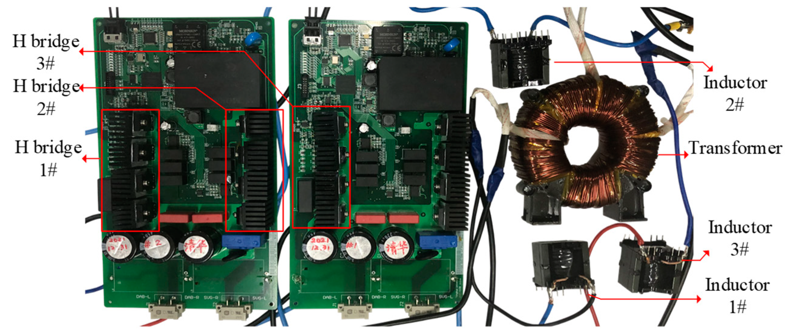
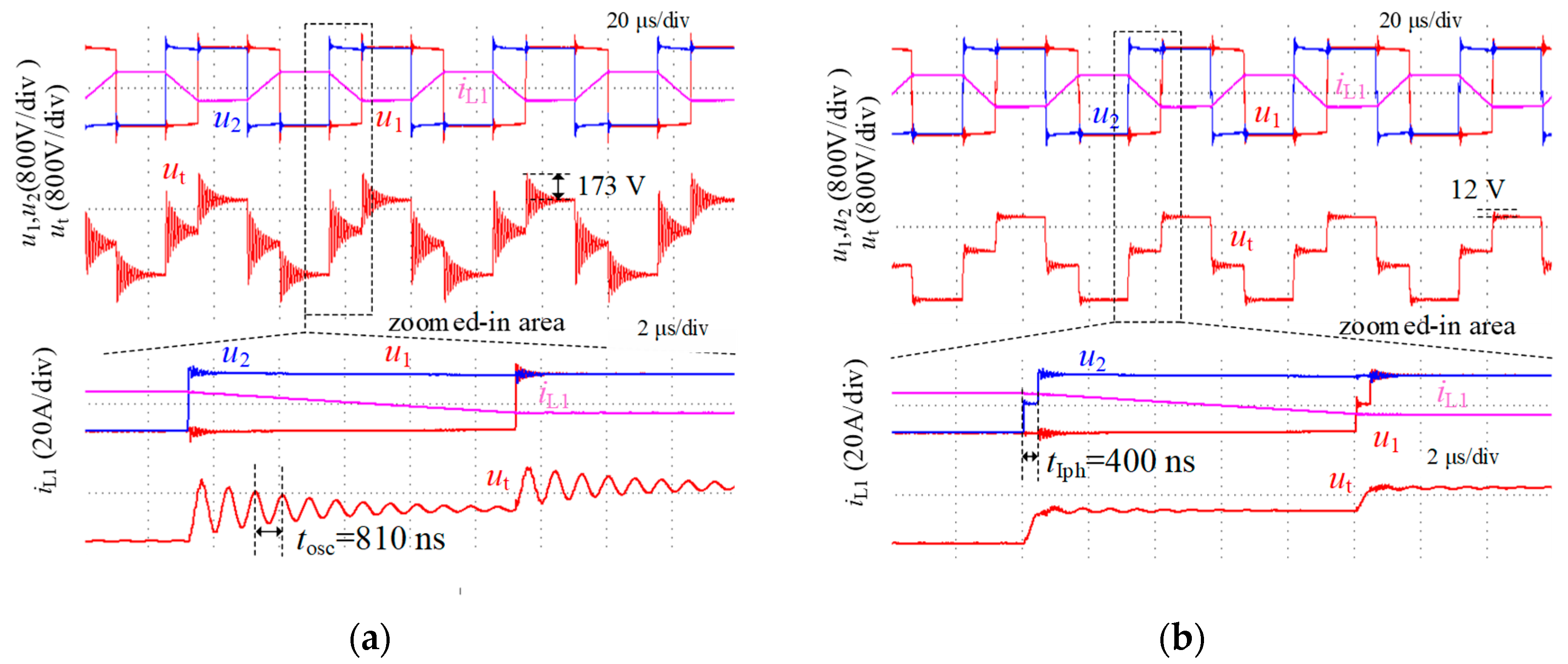
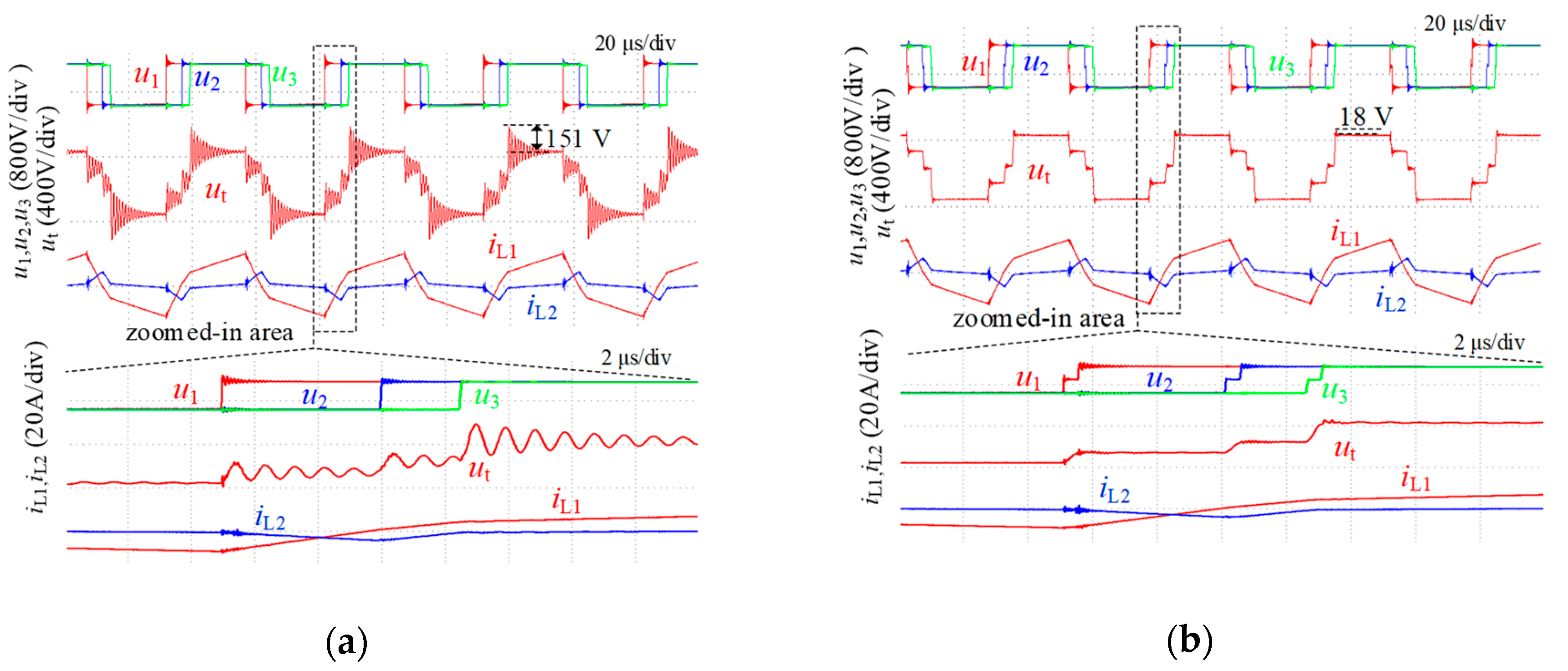
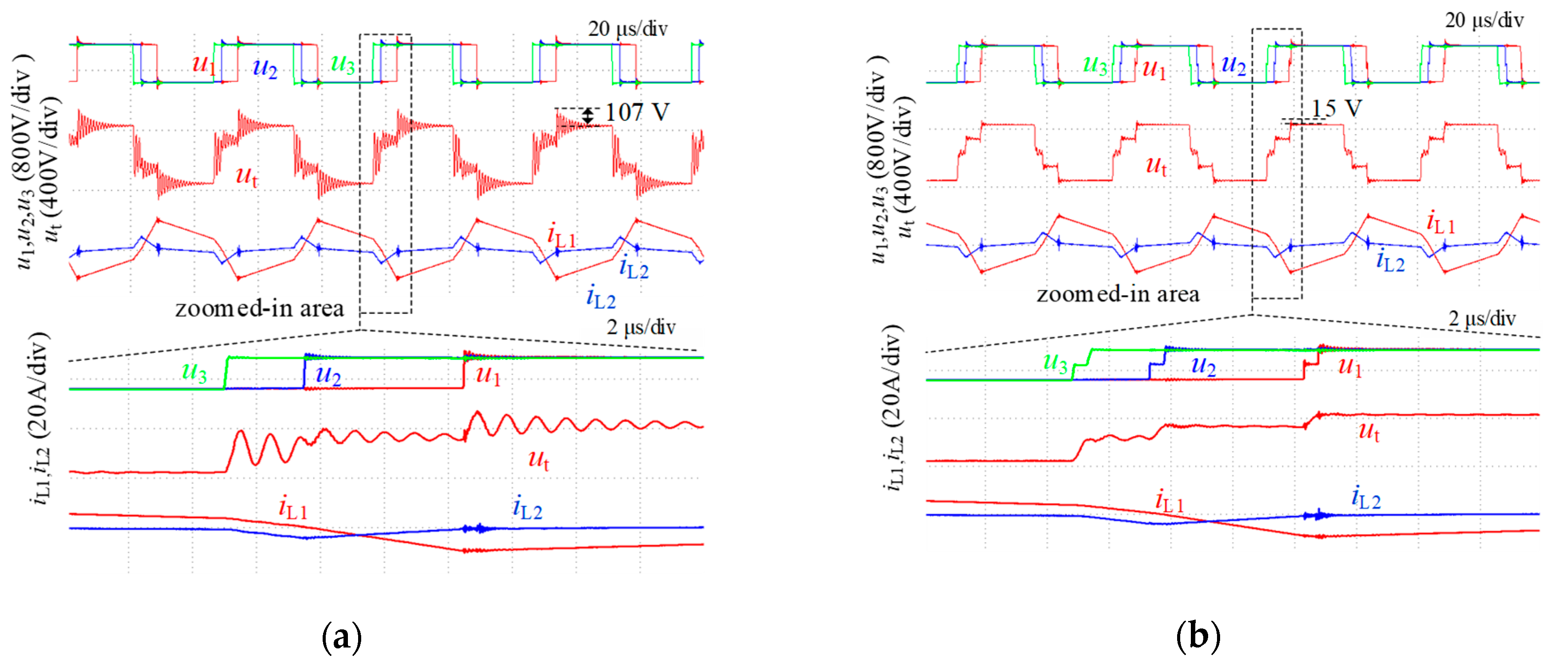
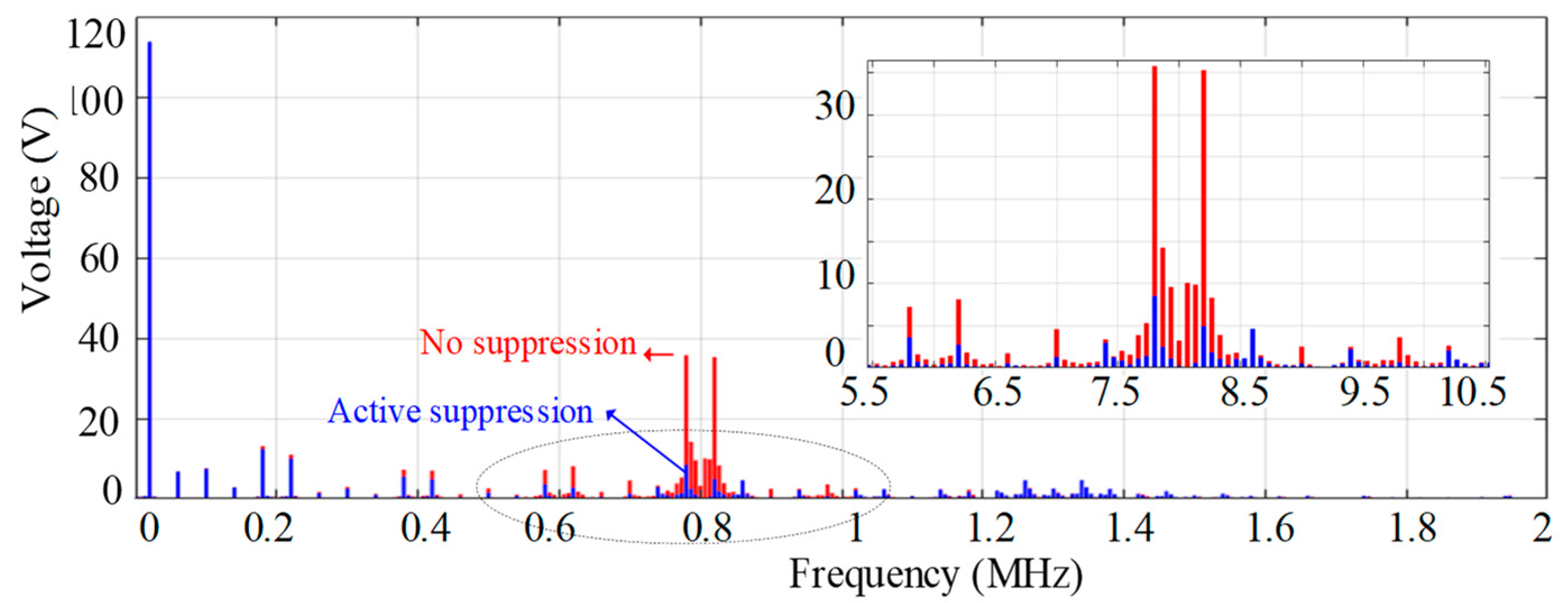
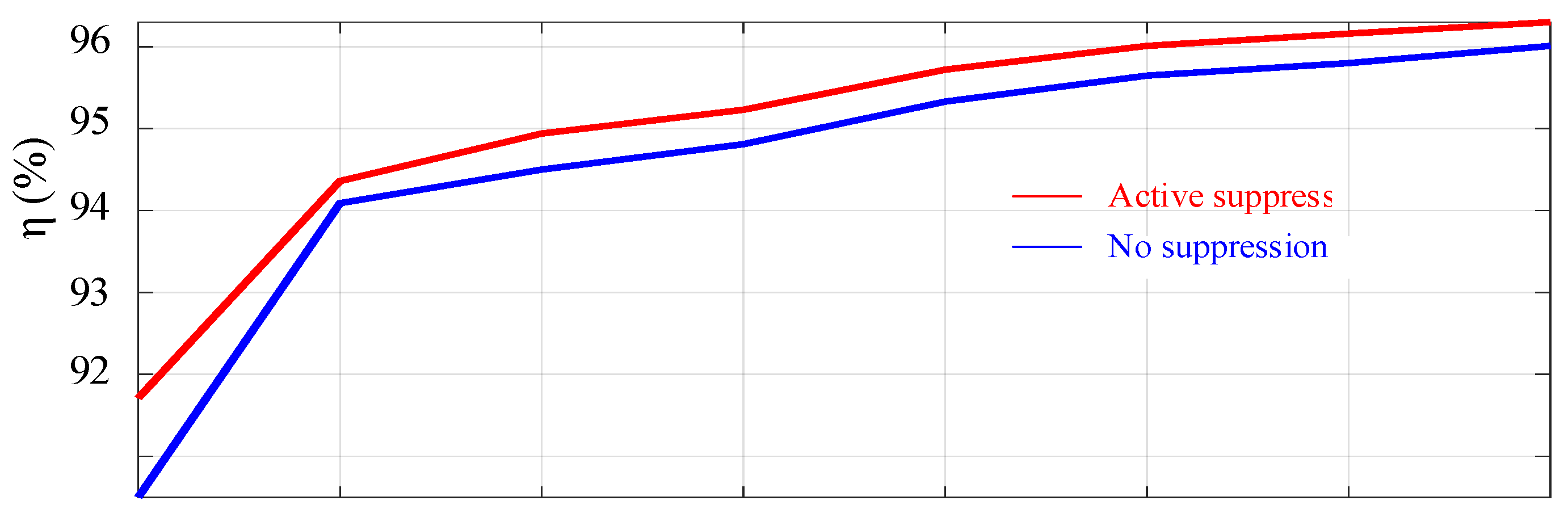
5. Experimental Validation

The TAB prototype described in the article was set up to verify the proposed method, which is shown in Figure 11. The SiC MOSFET from Cree C3M0075120K (1200 V 23 A) was utilized as the switching device in the H bridge. Nanocrystalline alloy magnetic core VAC W342 was used to make the transformer. It was convenient to set up the DAB converter by replacing the three-windings transformer with a two-windings transformer.
Figure 12 shows the waveforms of the DAB prototype for the forward power flow: VP1 = VP2 = 250 V. The phase shift duty between the primary side and second side was 0.4. The VSA was 238 V. Figure 8b shows the waveforms after the SHE PS modulation method was utilized. The inner phase-shift time was 400 ns, which was half of the oscillation period. The VSA was reduced by 94.1% from 238 V to 14 V.
Figure 13 shows the waveforms for the reverse power flow. The phase-shift duty between the primary side and second side was −0.4. The VSA was 173 V. Figure 13b shows the waveforms after the SHE PS modulation method was utilized. The inner phase-shift time was 400 ns, which was half of the oscillation period. The VSA was reduced by 93.1% from 173 V to 12 V.
Figure 14 shows the waveforms of the TAB prototype: VP1 = VP2 = VP3 = 250 V. The phase shift duties D1, D2 and D3 were 0, 0.2 and 0.3, respectively. The oscillation period was 0.92 μs. Figure 14b shows the waveforms after the SHE PS modulation method was utilized. The inner phase-shift time tIph was 460 ns, which was half of the oscillation period. The VSA was reduced by 92.1% from 151 to 18 V.
Figure 15 shows that the waveforms with the phase-shift duties D1, D2 and D3 were 0, −0.2 and −0.3, respectively. Figure 15b shows the waveforms after SHE PS modulation method was utilized. The VSA was reduced by 86.0% from 107 to 15 V. Figure 16 shows that the waveforms with the phase-shift duties D1, D2 and D3 were 0, 0.2 and −0.3, respectively. The VSA was reduced by 77.8% from 63 to 14 V.
Figure 17 shows the harmonics spectrum of the transformer voltage ut in the TAB in Figure 14. The harmonics around the oscillation frequency were obvious mitigated where the amplitude of the harmonics with the oscillation frequency was decreased by 77.1% from 35 V to 8 V when the SHE PS method was utilized.
The efficiency curve of the DAB prototype is shown in Figure 18, where VP1 = VP2 = 220 V. When the HFO was suppressed, the efficiencies were increased by 0.3~0.4% after the SHE PS modulation method was utilized.

6. Conclusions

This article studied the HFO of active-bridge-transformer-based DC/DC converters including DAB and MAB converters. Ignoring the AC resistance in the circuit, the high-order model of the voltage oscillation could be reduced to a second-order system. On top of that, a simplified and general HFO model for DABs and MABs with asymmetrical inductances was proposed. Then, the HFO was analyzed from a time domain prospective. Finally, a universal active SHE PS modulation method to suppress oscillation was investigated. Finally, the effectiveness and generality of the method were verified by DAB and MAB experimental results. To summarize, the SHE PS modulation suppression was applicable for DAB and MAB. No additional circuits were required to mitigate the HFO problem for the existing equipment, so redesigning or changing the transformers and inductors was not needed. It was easy to implement. This simple short-circuit test could be used to pre-obtain the inner phase-shift as well as for the accurate measurement of the stray parameters.

Author Contributions

Conceptualization, S.W. and W.W.; methodology, S.W.; software, S.W.; validation, W.W.; formal analysis, W.W.; investigation, W.W.; resources, S.W.; data curation, S.W.; writing—original draft preparation, S.W.; writing—review and editing, S.W.; visualization, S.W.; supervision, W.W.; project administration, W.W.; funding acquisition, W.W. All authors have read and agreed to the published version of the manuscript.

Funding

This research was supported by the key project of Science and Technology Innovation Program of Army Engineering University of PLA under Grant KYCQJQZL2119.

Data Availability Statement

Not applicable.

Conflicts of Interest

The authors declare no conflict of interest.

References

  1. Hou, N.; Li, Y. Overview and comparison of modulation and control strategies for non-resonant single-phase dual-active-bridge dc-dc converter. IEEE Trans. Power Electron. 2020, 35, 3148–3172. [Google Scholar] [CrossRef]
  2. Michal, G.; Lech, M.G.; Kaszewski, A. A Dual Rising Edge Shift Algorithm for Eliminating the Transient DC-Bias Current in Transformer for a Dual Active Bridge Converter. Energies 2021, 14, 4264. [Google Scholar]
  3. Bandyopadhyay, S.; Purgat, P.; Qin, Z. A Multi-active Bridge Converter with Inherently Decoupled Power Flows. IEEE Trans. Power Electron. 2021, 36, 2231–2245. [Google Scholar] [CrossRef]
  4. Falcones, S.; Ayyanar, R.; Mao, X. A DC–DC Multiport-Converter-Based Solid-State Transformer Integrating Distributed Generation and Storage. IEEE Trans. Power Electron. 2013, 28, 2192–2203. [Google Scholar] [CrossRef]
  5. Tehrani, K.; Yunbi, L.I.; Rousseau, L.; Normand, A.; Vurpillot, F. Design of A Multistage Marx Generator Topology based on SiC-MOSFET Device for Atomic Probe Tomography Applications. In Proceedings of the 2020 IEEE 15th International Conference of System of Systems Engineering SoSE, Budapest, Hungary, 2–4 June 2020; pp. 423–428. [Google Scholar]
  6. Tuluhong, A.; Wang, W.; Li, Y.; Wang, H.; Xu, L. Research on Modelling and Stability Characteristics of Electric Traffic Energy System Based on ZVS-DAB Converter. J. Electr. Comput. Eng. 2020, 2020, 5450628. [Google Scholar] [CrossRef]
  7. Tehrani, K.; Weber, M.; Rasoanarivo, I. Design of High Voltage Pulse Generator with Back-to-Back Multilevel Boost Buck Converters Using SiC-MOSFET Switches. In Proceedings of the 2020 IEEE 15th International Conference of System of Systems Engineering SoSE, Budapest, Hungary, 2–4 June 2020; pp. 507–512. [Google Scholar]
  8. Cui, B.; Shi, H.; Sun, Q. A Novel Analysis Design and Optimal Methodology of High-Frequency Oscillation for Dual Active Bridge Converters with WBG Switching Devices and Nanocrystalline Transformer Cores. IEEE Trans. Power Electron. 2021, 36, 7665–7678. [Google Scholar] [CrossRef]
  9. Cui, B.; Xue, P.; Jiang, X. Elimination of High Frequency Oscillation in Dual Active Bridge Converters by dv/dt Optimization. IEEE Access 2019, 7, 55554–55564. [Google Scholar] [CrossRef]
  10. Qin, Z.; Shen, Z.; Blaabjerg, F. Transformer Current Ringing in Dual Active Bridge Converters. IEEE Trans. Ind. Electron. 2021, 68, 12130–12140. [Google Scholar] [CrossRef]
  11. Hassan, I.; Keshmiri, N.; Dorneles, A. Design Optimization Methodology for Planar Transformers for More Electric Aircraft. IEEE Open J. Ind. Electron. Soc. 2021, 2, 568–583. [Google Scholar] [CrossRef]
  12. Wang, C.; Zsurzsan, G.T.; Zhang, Z. Genetic Algorithm Assisted Parametric Design of Splitting Inductance in High Frequency GaN-based Dual Active Bridge Converter. IEEE Trans. Ind. Electron. 2021, 1. [Google Scholar] [CrossRef]
  13. Wei, S.; Zhao, Z.; Yuan, L. Voltage Oscillation Suppression for the High-Frequency Bus in Modular-Multiactive-Bridge Converter. IEEE Trans. Power Electron. 2021, 36, 9737–9742. [Google Scholar] [CrossRef]
  14. Farhangi, B.; Toliyat, H.A. Modeling and Analyzing Multiport Isolation Transformer Capacitive Components for Onboard Vehicular Power Conditioners. IEEE Trans. Ind. Electron. 2015, 62, 3134–3142. [Google Scholar] [CrossRef]
  15. Alawieh, H.; Riachy, L.; Tehrani, K.A.; Azzouz, Y.; Dakyo, B. A new dead-time effect elimination method for H-bridge inverters. In Proceedings of the IECON 2016—42nd Annual Conference of the IEEE Industrial Electronics Society, Florence, Italy, 23–26 October 2016; pp. 3153–3159. [Google Scholar]
Figure 1. HFO in a MAB converter prototype: (a) TAB circuit; (b) waveforms.
Energies 15 03311 g001
Figure 2. Equivalent HF circuit considering the stray parameters of the transformer. (a) DAB converter; (b) MAB converter.
Energies 15 03311 g002
Figure 3. Thevenin equivalent circuit.
Energies 15 03311 g003
Figure 4. DAB circuit with external AC resistors.
Energies 15 03311 g004
Figure 5. Bode plot of the voltage transfer function with different AC resistances.
Energies 15 03311 g005
Figure 6. Experimental voltage waveform with different AC resistances.
Energies 15 03311 g006
Figure 7. Short-circuit test. (a,c) Test circuit and waveforms of the DAB converter; (b,d) test circuit and waveforms of the TAB converter.
Energies 15 03311 g007
Figure 8. Output voltage of the active bridge. (a) H bridge; (b) output voltage.
Energies 15 03311 g008
Figure 9. Oscillation amplitude vs. inner phase-shift.
Energies 15 03311 g009
Figure 10. Simulated waveforms with different splitting inductances. (a) Transformer voltage; (b) transformer current.
Energies 15 03311 g010
Figure 11. Experimental prototype.
Energies 15 03311 g011
Figure 12. Waveforms of the DAB converter with forward power flow (D = 0.4): (a) no suppression; (b) with the SHE PS method.
Energies 15 03311 g012
Figure 13. Waveforms of the DAB converter with reverse power flow (D = −0.4): (a) no suppression; (b) with SHE PS method.
Energies 15 03311 g013
Figure 14. Waveforms of the TAB converter with forward power flow (D1 = 0, D2 = 0.2, D3 = 0.3): (a) no suppression; (b) with the SHE PS method.
Energies 15 03311 g014
Figure 15. Waveforms of the TAB converter with reverse power flow (D1 = 0, D2 = −0.2, D3 = −0.3): (a) no suppression; (b) with SHE PS method.
Energies 15 03311 g015
Figure 16. Waveforms of the TAB converter with reverse power flow (D1 = 0, D2 = 0.2, D3 = −0.3): (a) no suppression; (b) with the SHE PS method.
Energies 15 03311 g016
Figure 17. Harmonics spectrum of the transformer voltage in the TAB converter.
Energies 15 03311 g017
Figure 18. Efficiency curve of the DAB prototype.
Energies 15 03311 g018
Table 1. Parameters of the DAB and MAB prototypes.
ParametersDAB ConverterTAB Converter
Swithing devicesC3M0075120K(SiC MOSFET)C3M0075120K (SiC MOSFET)
Swithing frequency20 kHz20 kHz
Transformer turn ratioN1:N2 = 1:1N1:N2:N3 = 4:5:6
Transformer capacitancesC1 = C2 = 130 pF, C12 = 55 pFC1 = 85 pF, C2 = 100 pF, C3 = 140 pF,C12 = 70 pF, C23 = 70 pF, C13 = 70 pF
Transformer leakage inductanceLS1 = 3 μH, LS2 = 3 μHLS1 = 3 μH, LS2 = 3.5 μH, LS2 = 4 μH
Transformer winding resistanceRS = 0.016 ΩRS1 = 0.03 Ω, RS = 0.035 Ω, RS = 0.05 Ω
Transformer magnetizing inductanceLm = 63 mHLm = 24 mH
Transformer magnetizing resistorRm = 10 kΩRm = 25 kΩ
Phase-shift inductanceL1 = 160 μH, L2 = 100 μHL1 = 140 μH, L2 = 160 μH, L3 = 100 μH
Equivalent resistanceR1 = 0.016 Ω, R2 = 0.016 Ω R1 = 0.016 Ω, R2 = 0.016 Ω, R3 = 0.016 Ω
Table 2. Overall comparison with other methods.
MethodsModeApplicable TopologyBranch ParametersImplementation Complexity
[8,9]PassiveDABOnly symmetrical parameters are considered.Moderate
[10]PassiveDABOnly asymmetrical parameters are considered with N 1 : N 2   1 Moderate
[11]PassiveDABOnly asymmetrical parameters are considered.Difficult
[12]PassiveDABOnly asymmetrical parameters are considered with N 1 : N 2   1 Moderate
[13]ActiveModular MABOnly symmetrical parameters are considered.Easy
Proposed methodActiveDAB, MABEffective with both the symmetrical and asymmetrical parametersEasy
Publisher’s Note: MDPI stays neutral with regard to jurisdictional claims in published maps and institutional affiliations.

