

Performance Analysis and Evaluation of Multiphase Split-Source Inverters
 , ,
, , 

Abstract
:1. Introduction
- -
- Regardless of the input voltage, the voltage gain, , can be improved by producing any desired AC output voltage, even that greater than the line voltage.
- -
- No additional circuits are needed to provide ride-through during voltage sags.
- -
- This reduces the line’s common-mode voltage and harmonic current while improving the power factor.
- ○
- It has a continuous input current and DC-link voltage.
- ○
- It has lower voltage stresses across the switches for high-voltage gains.
- ○
- It requires a lower passive component count.
- ○
- It uses the same switching states as the VSI, which uses a different state for ST.
- ○
- Compared with the two-stage architecture, no additional active switch is required in the SSI.
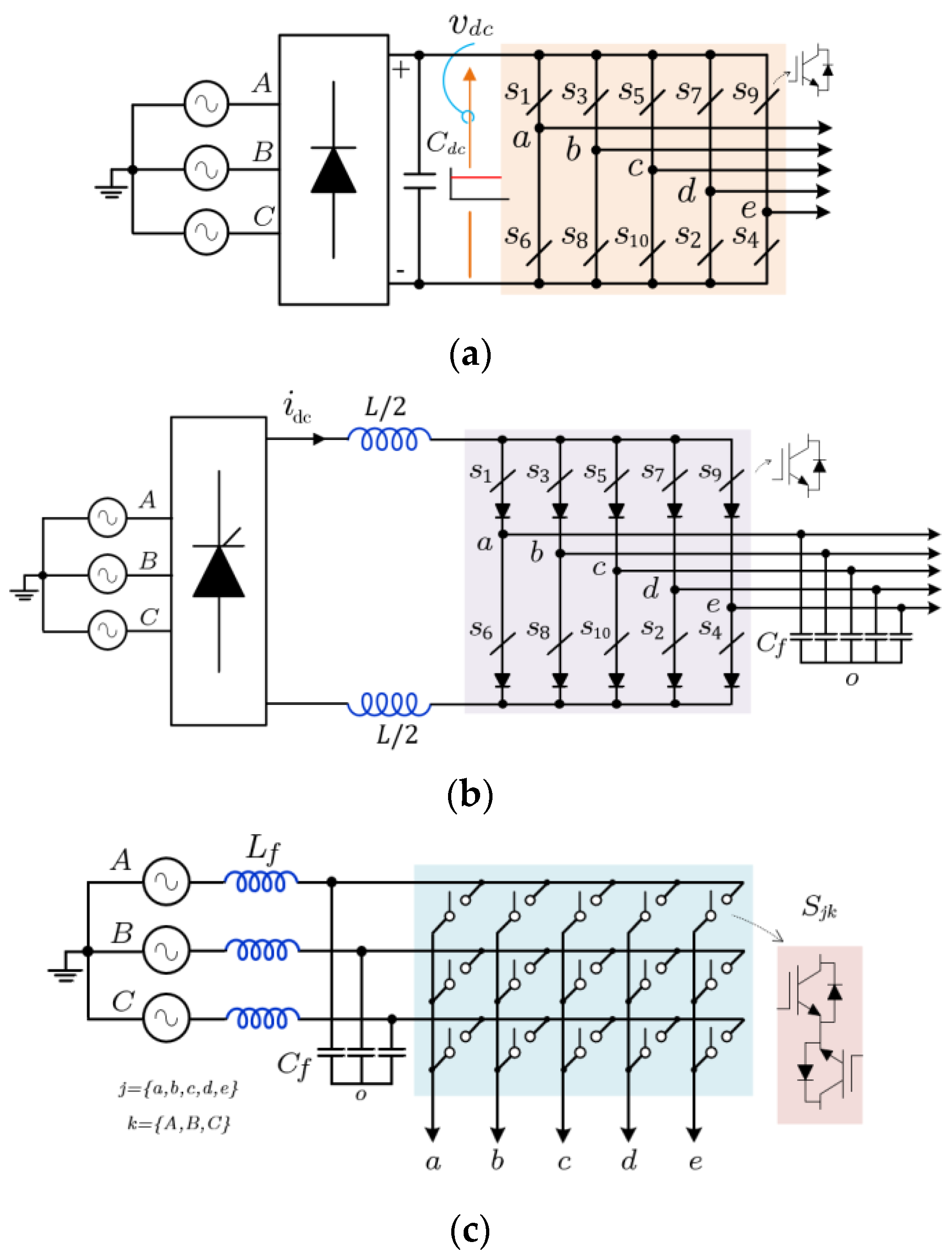
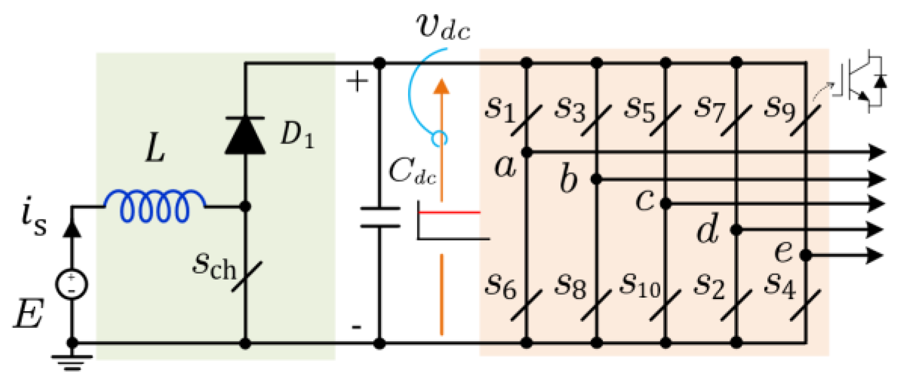
2. Review of Three-Phase Split-Source Inverters
2.1. Topology
2.2. Operation
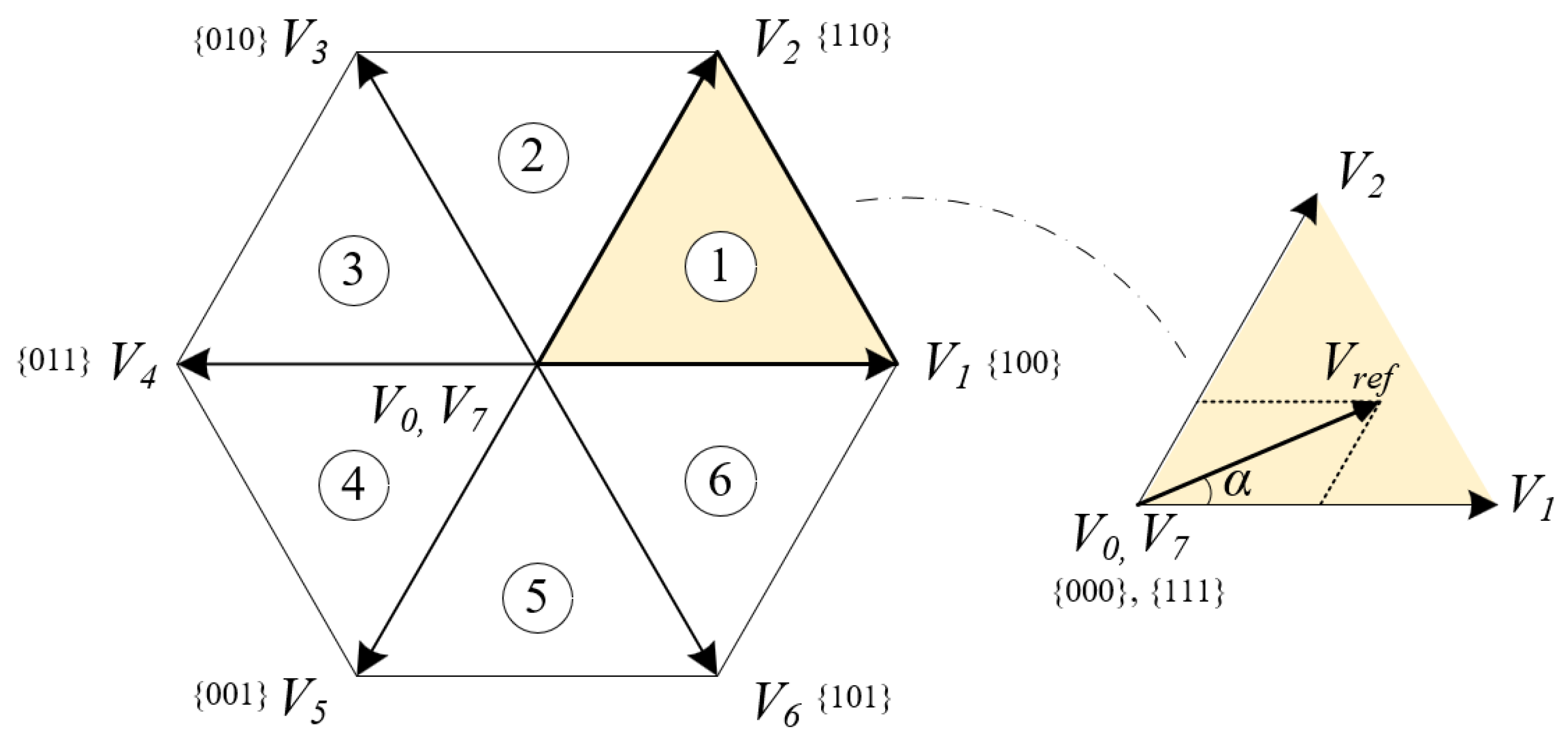
- (1)
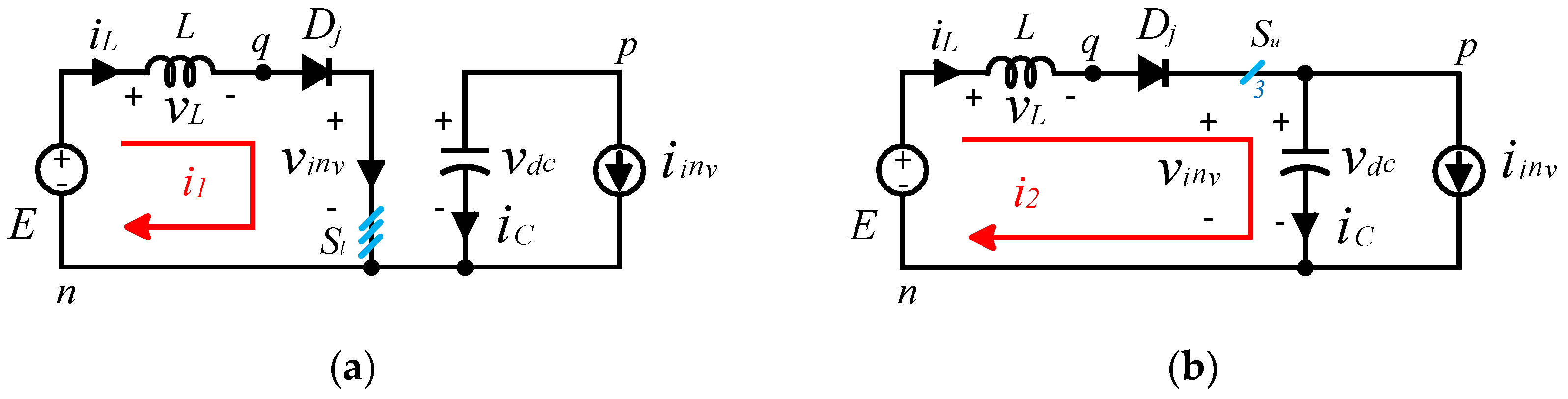
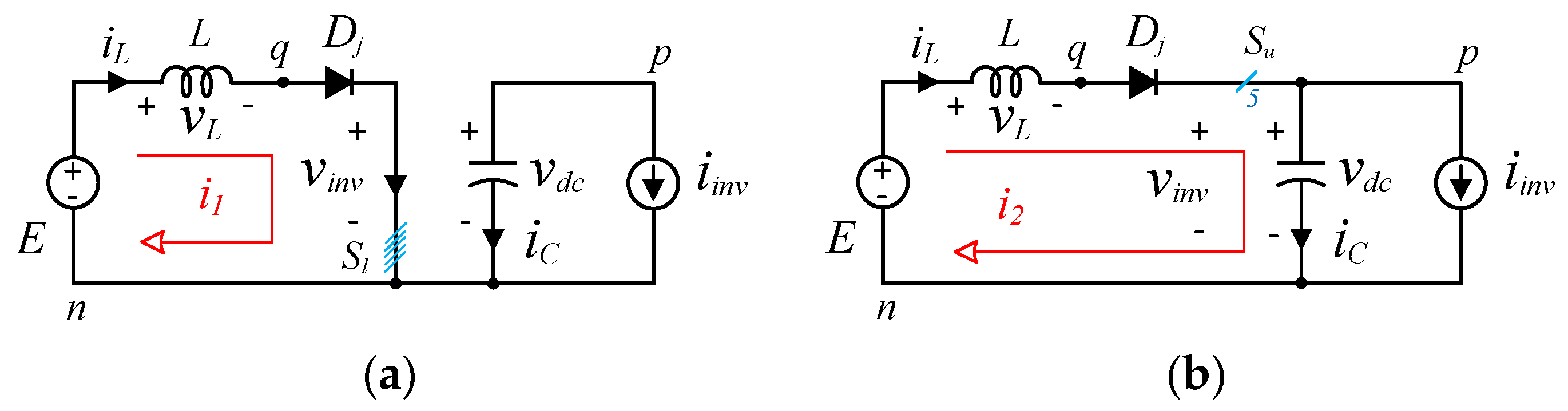
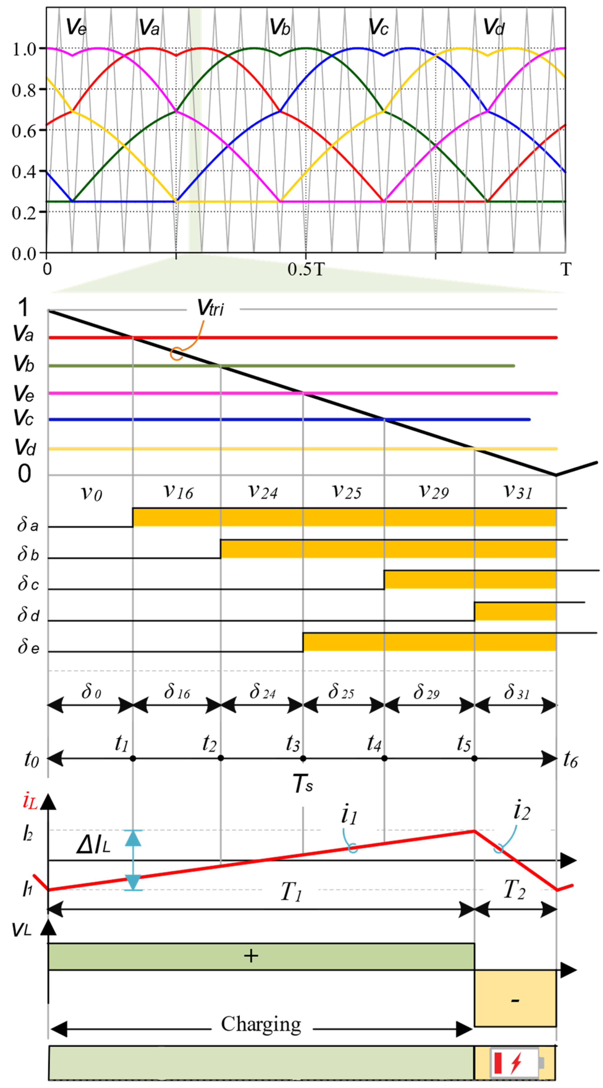
- Inductive Charging Mode: The charging mode can be obtained by switching ON at least one of the lower switches in the B6 bridge. In this case, the voltage at the output of the DC-side is zero (i.e., ) due to the short circuit, as shown in Figure 5a. As a result, the inductor is charged during an interval of .
- (2)
- Inductive Discharging Mode: The discharging mode occurs when all of the upper switches in the B6 bridge are turned ON (i.e., V7{111}). In this case, the inductor will release its energy in the capacitor via the antiparallel diodes of the upper switches during an interval of , where , is the sampling time. Hence, the voltage at the DC side equals the capacitor voltage (i.e.,), as shown in Figure 5b.
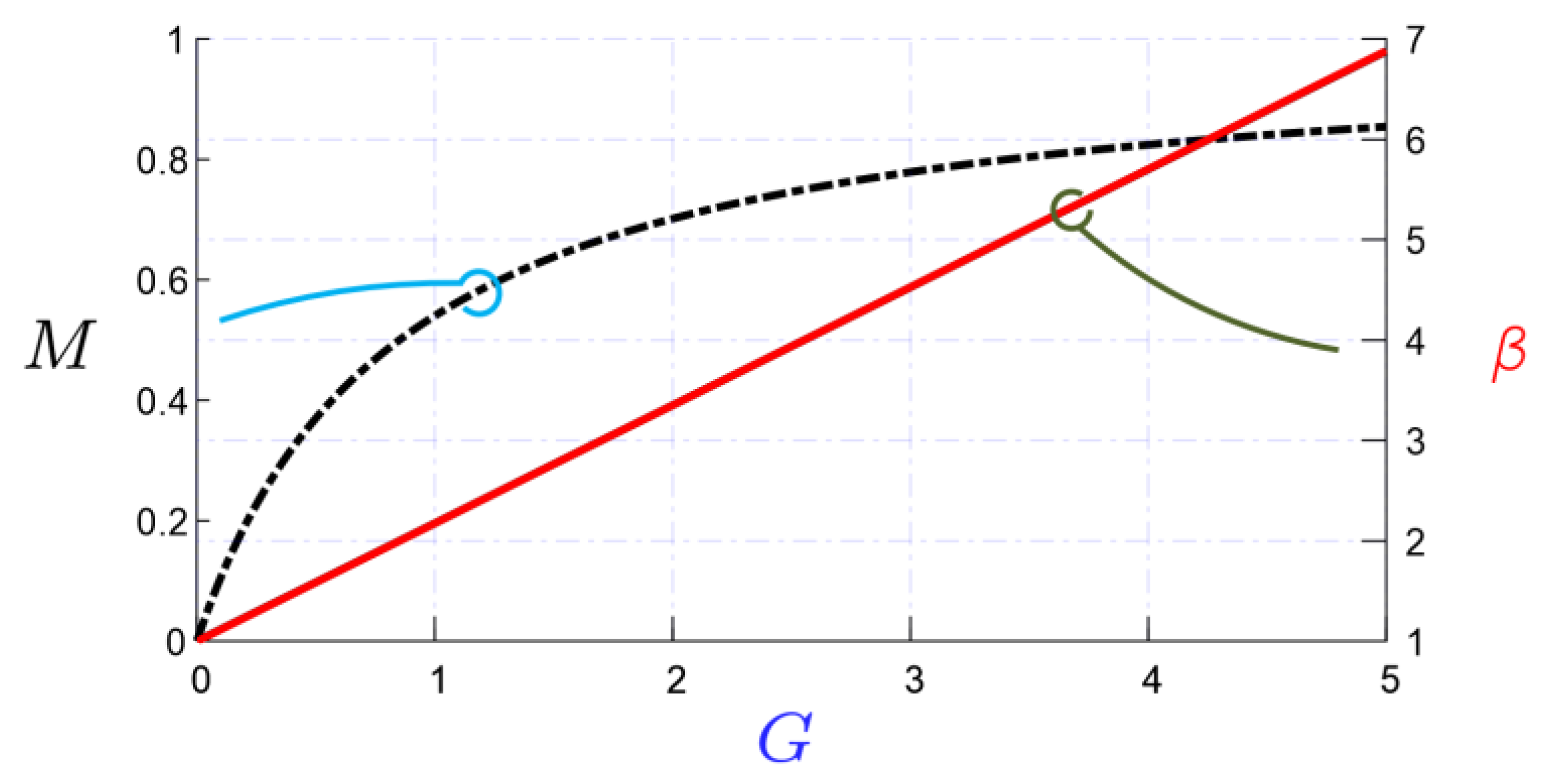
2.3. DC Boosting Factor
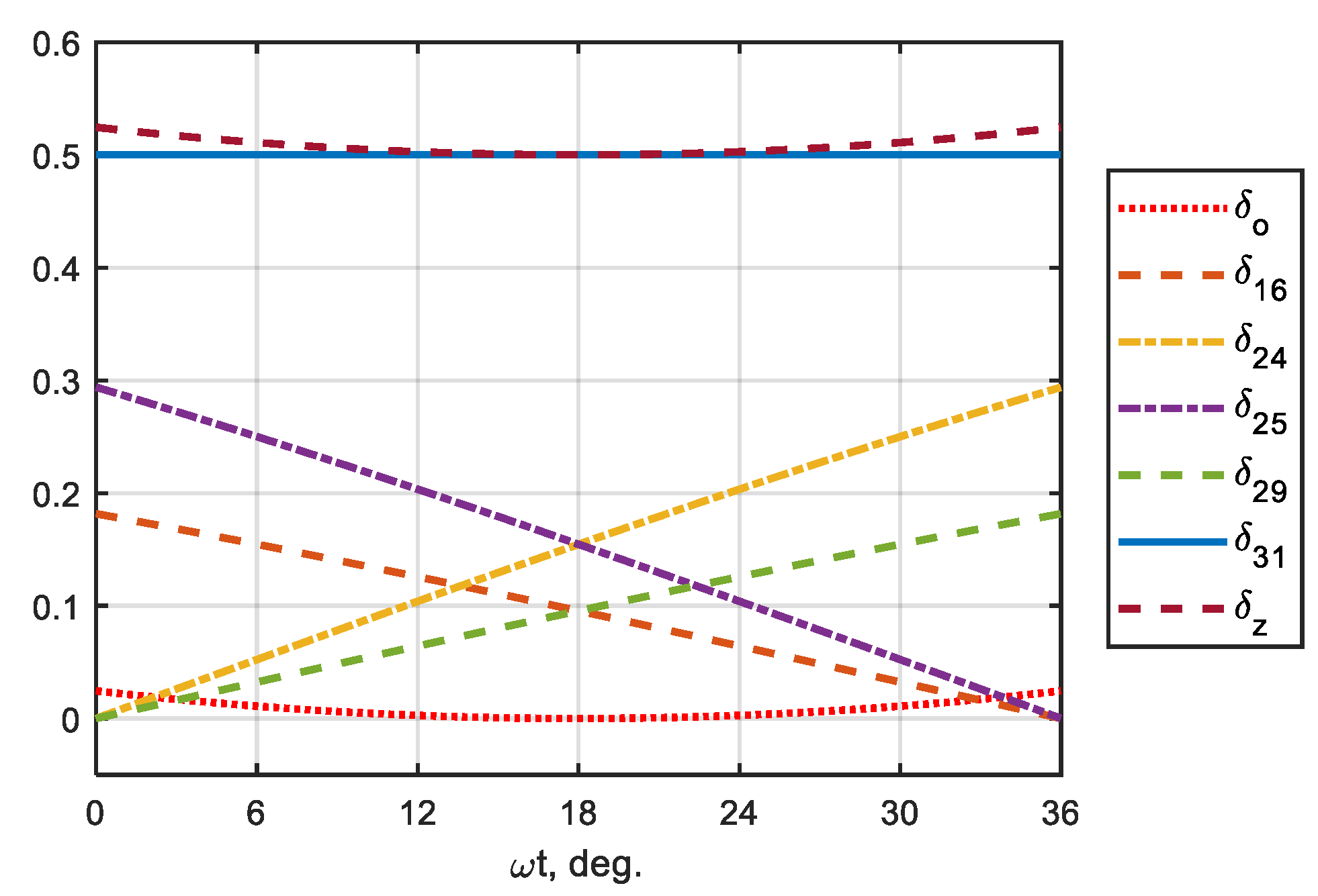
2.4. Modulation
2.5. Design Procedure
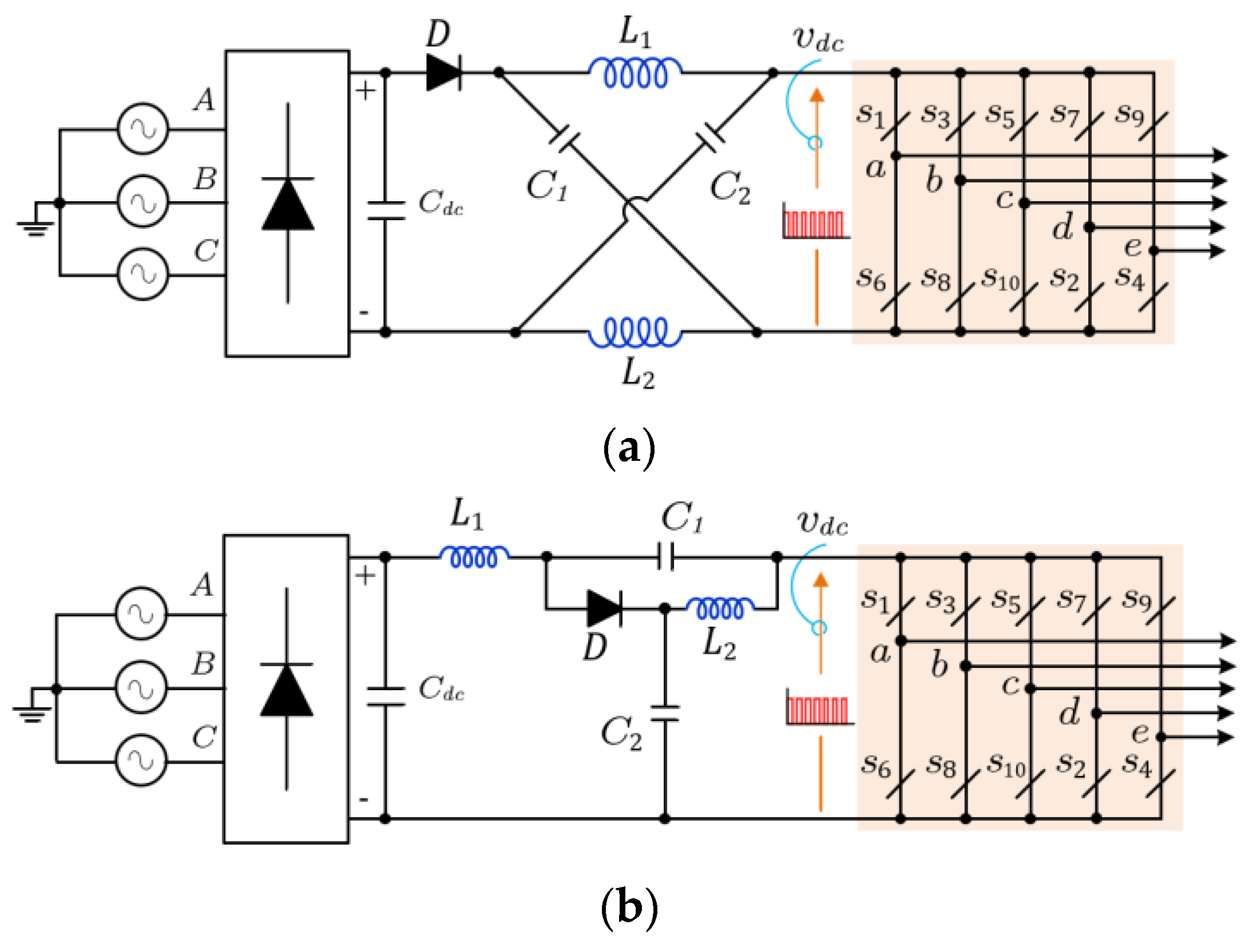
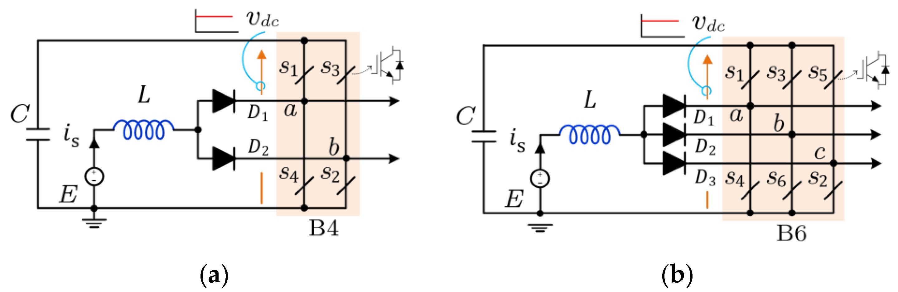
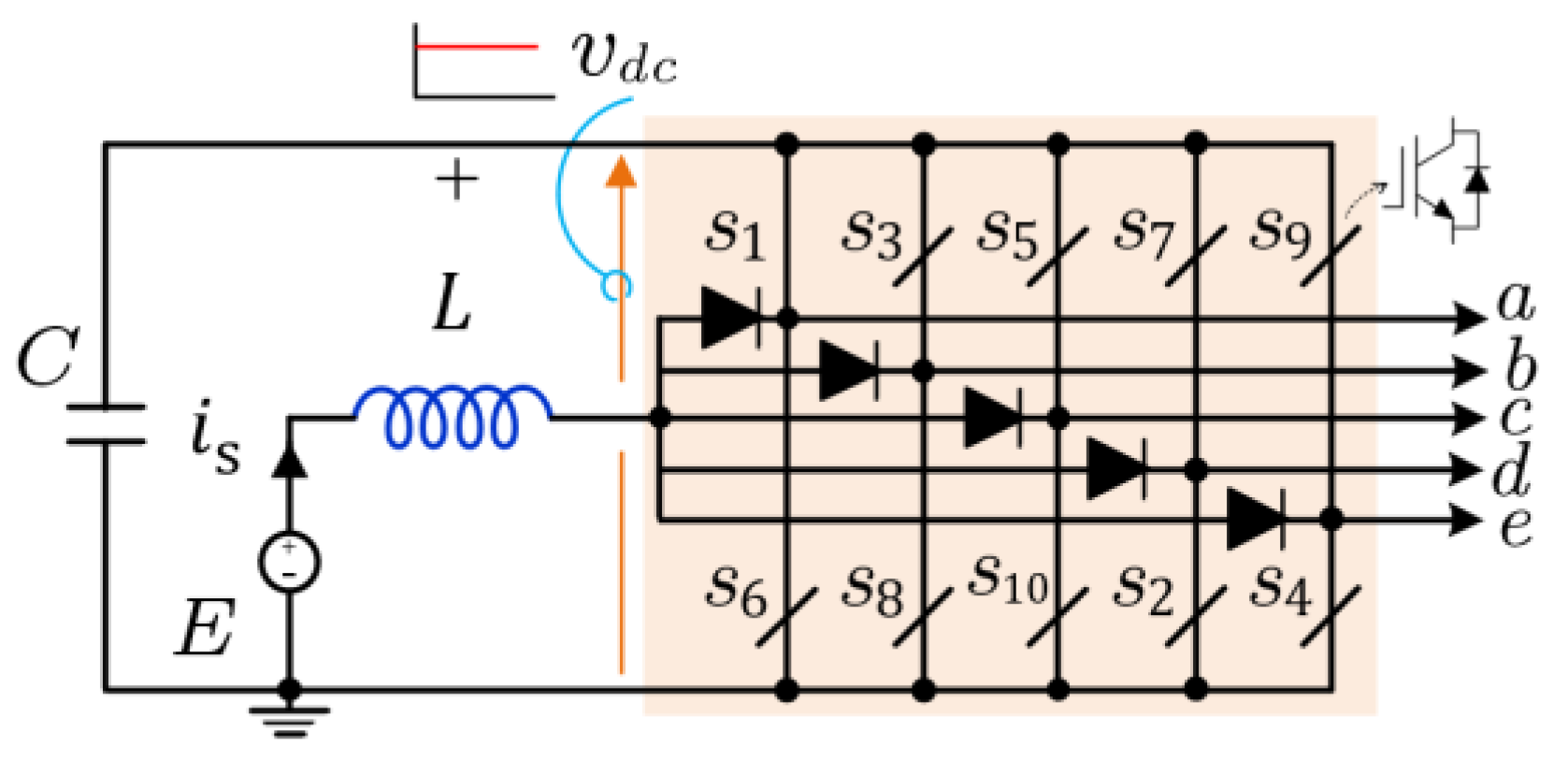
3. Proposed Five-Phase Split-Source Inverters
4. Current Ripple Analysis of Five-Phase SSI
4.1. DC Ripple and Design of Passive Components
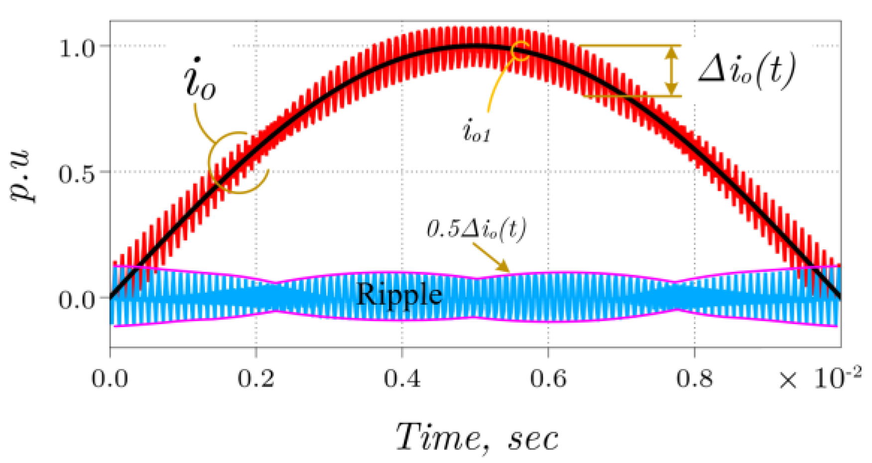
4.2. AC Current Ripple
- ○
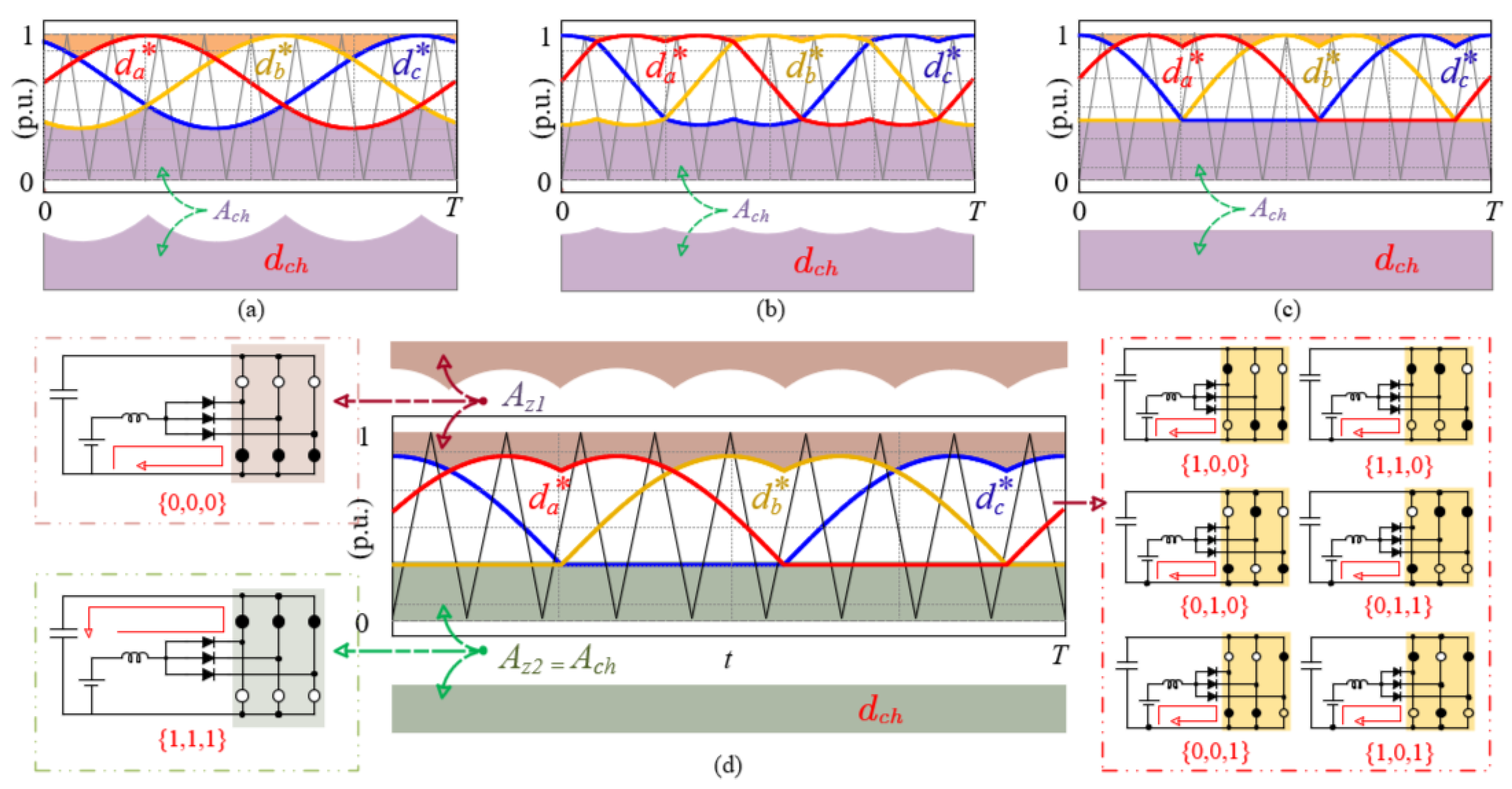
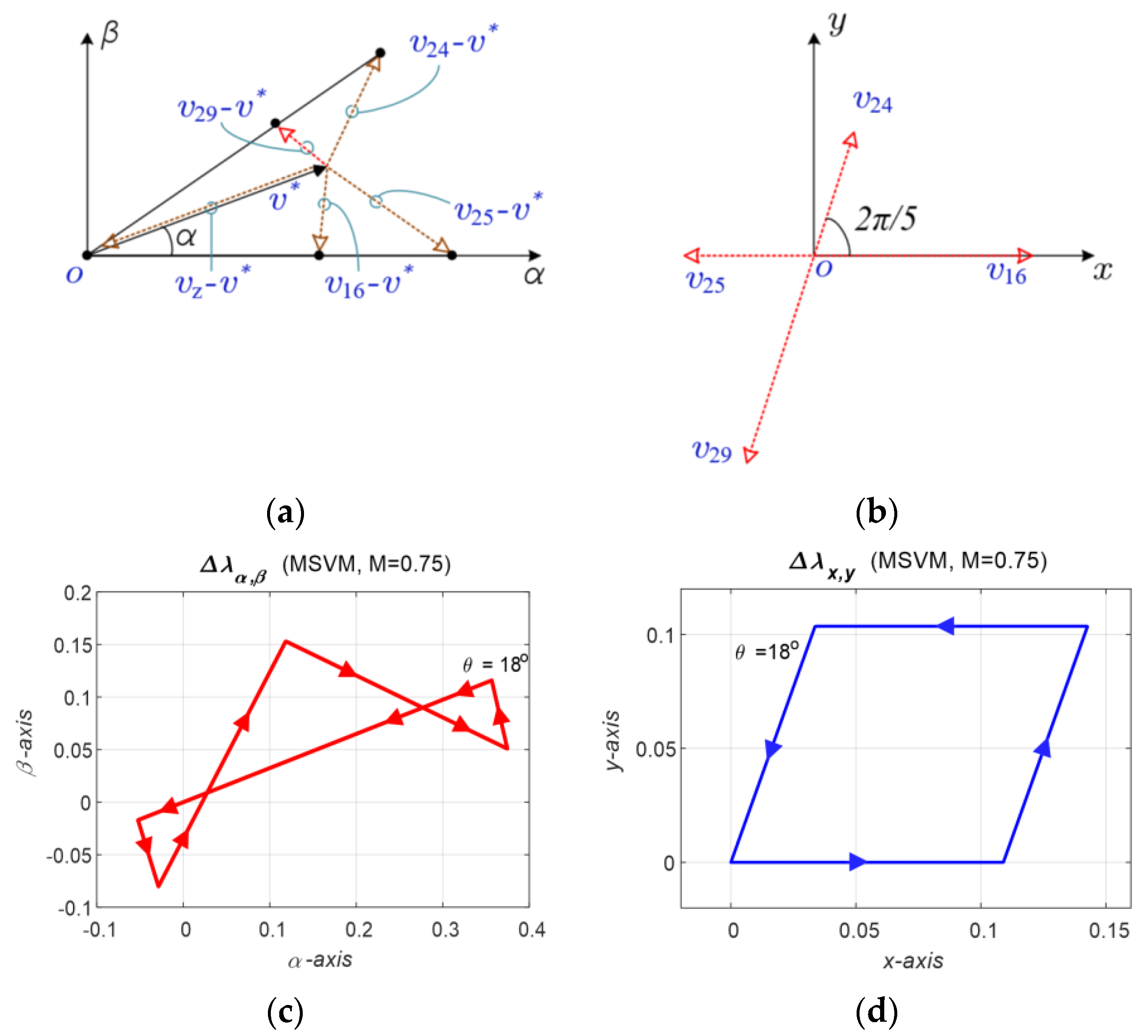
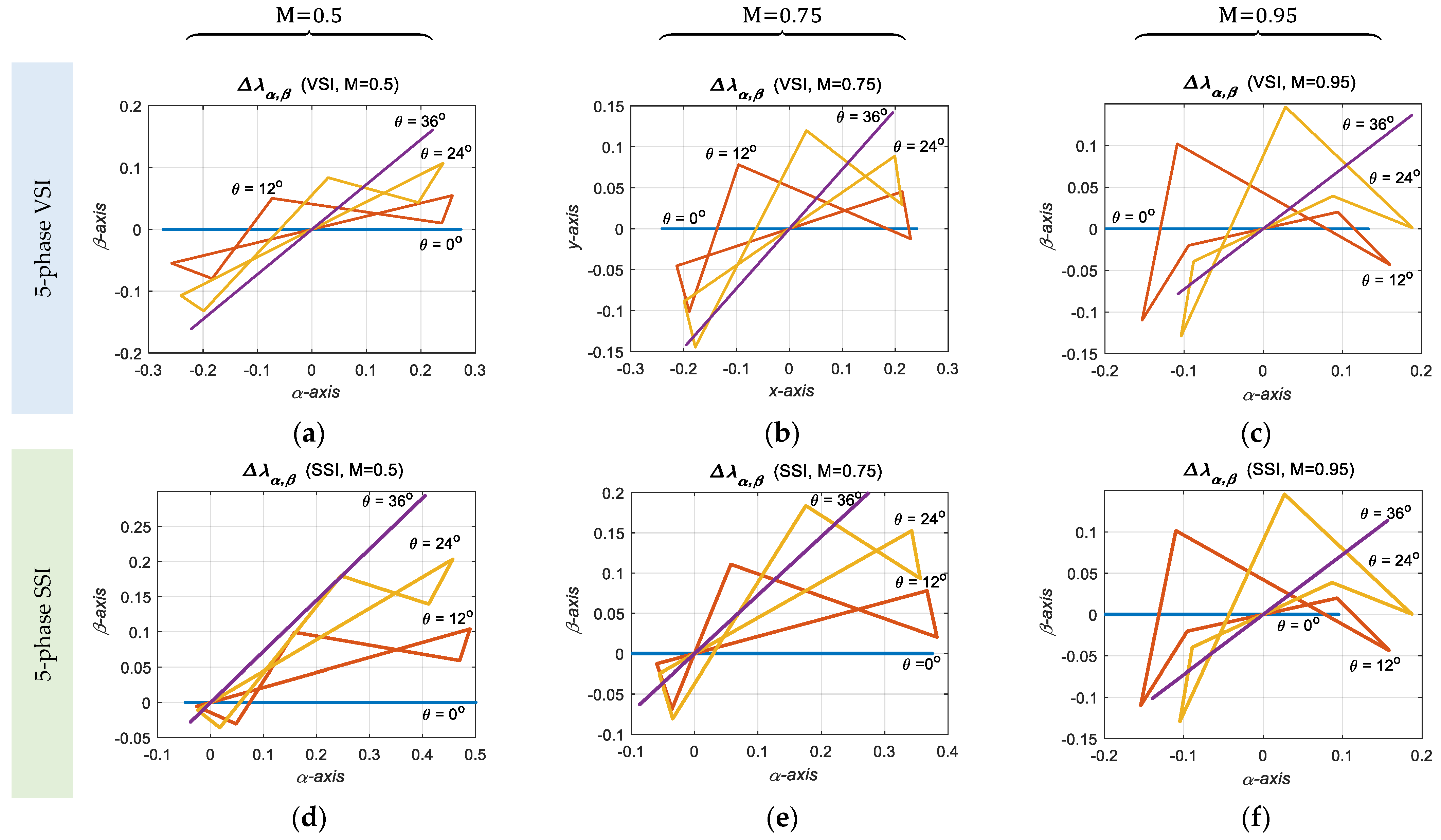
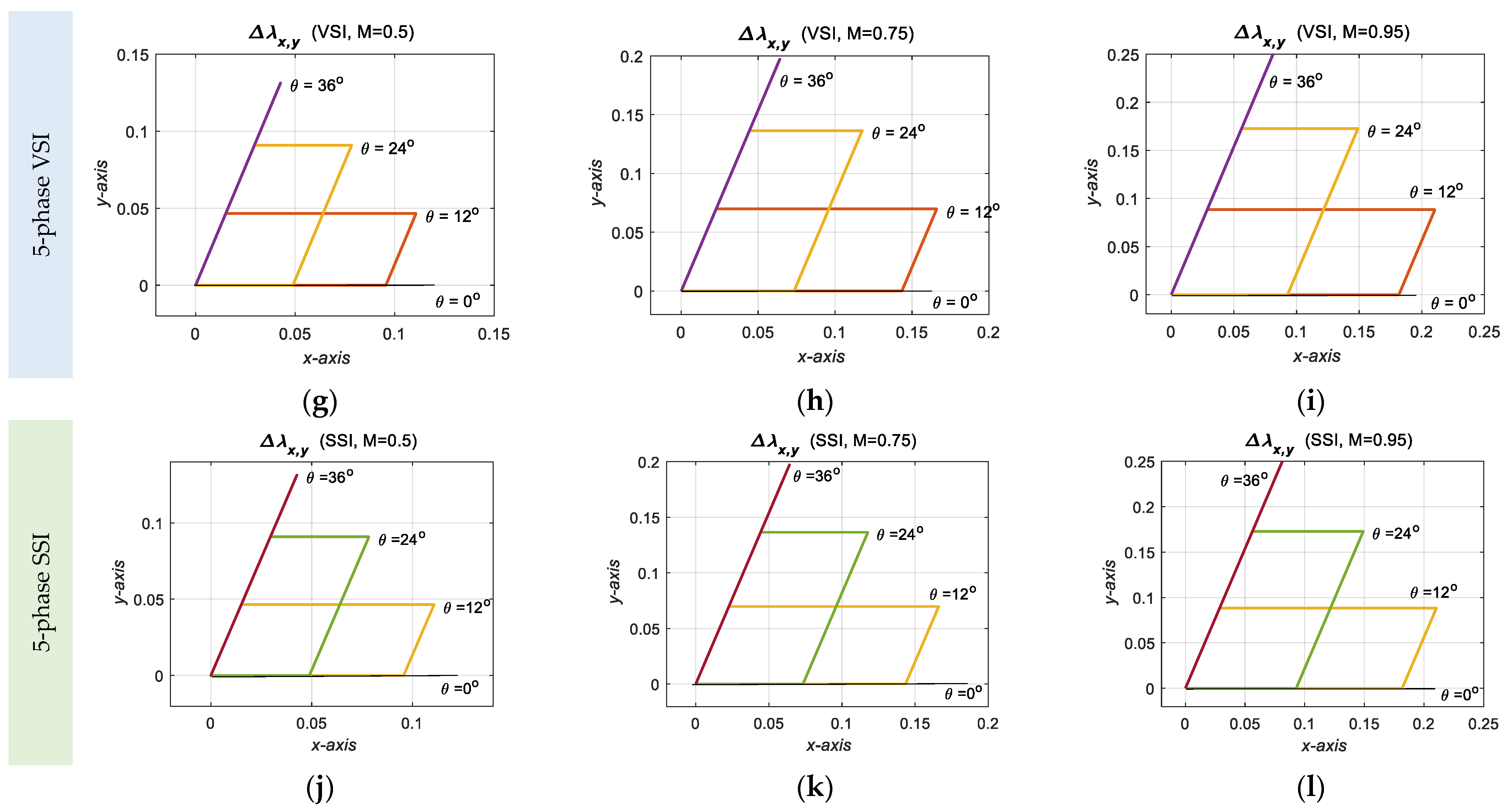
- Due to the symmetrical distribution of the zero vectors in the classical SVM of VSI, symmetrical harmonic flux trajectories are observed from the plane of Figure 15a–c, while there are some asymmetries in the MSVM for SSI because of the level shift approach, as shown in Figure 15d–f. However, the same trajectories are obtained in the plane, as shown in Figure 15g–l. This is owed to the zero references on this plane.
- ○
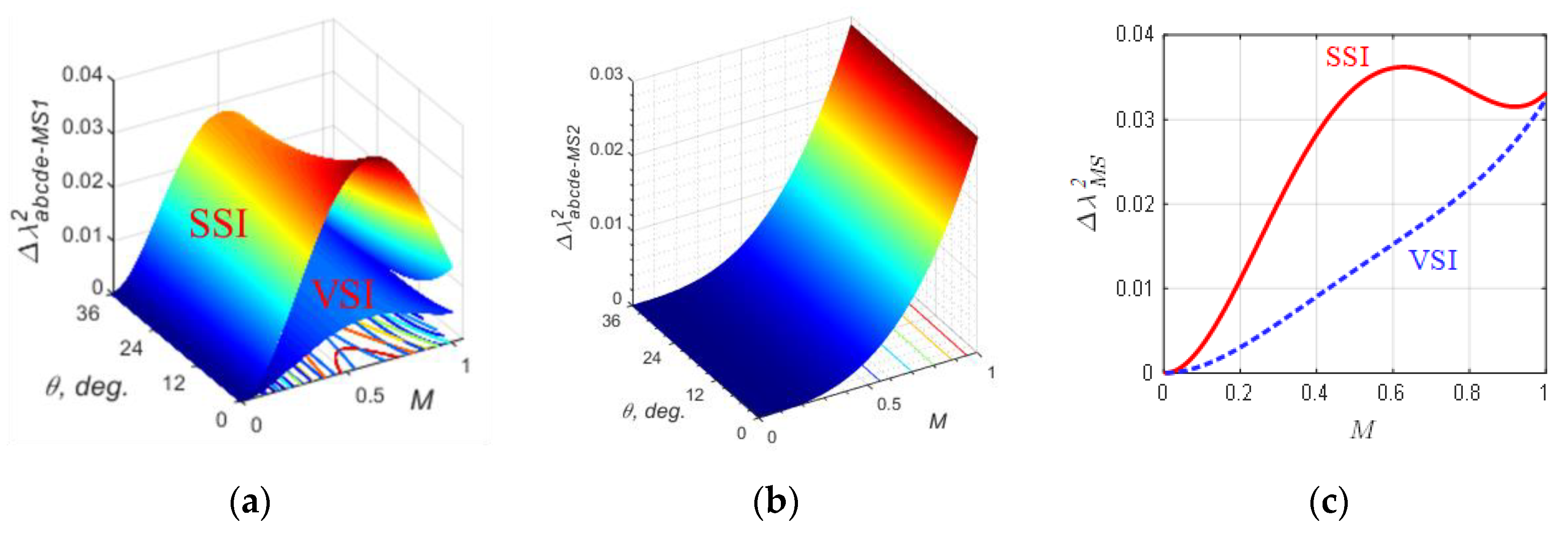
- As shown in Figure 16a,b, the HDF is significantly greater for SSI than for VSI in the -plane, particularly for low-modulation indices. However, in the -plane, the HDF is the same.
- ○
- Due to the elimination of the level shift effect on SSI modulating waveforms at M = 1, both VSI and SSI have approximately equal HDFs, as shown in Figure 16c.
- ○
- The SSI produces higher current ripples than the traditional VSI, but since the SSI also boosts the voltage, it does not require an additional DC booster.
5. Simulation and Experimental Results
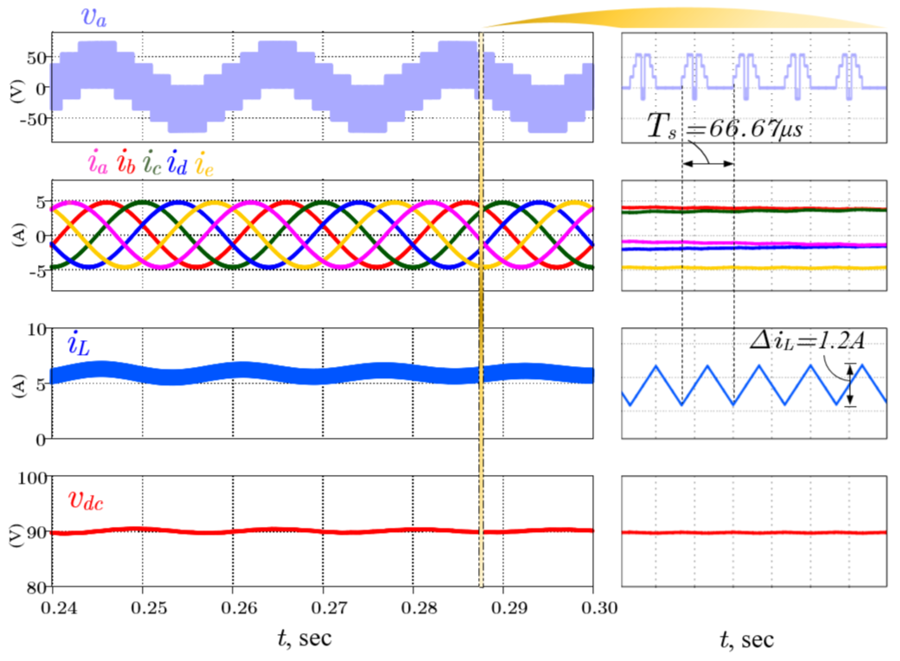
- The simulated waveforms and measured values from PLECS for the five-phase SSI show good agreement with that estimated from the analysis. For example, the average DC-link voltage is 90V, and the input current ripple 1.2 A agrees with that calculated from (13) and (16), respectively, at the given condition of the case study.
- The output-phase currents are sinusoidal waves, and the input current is completely free from the low-order harmonics. Moreover, the DC-link capacitor voltage exhibits near-constant value.
6. Experimental Results
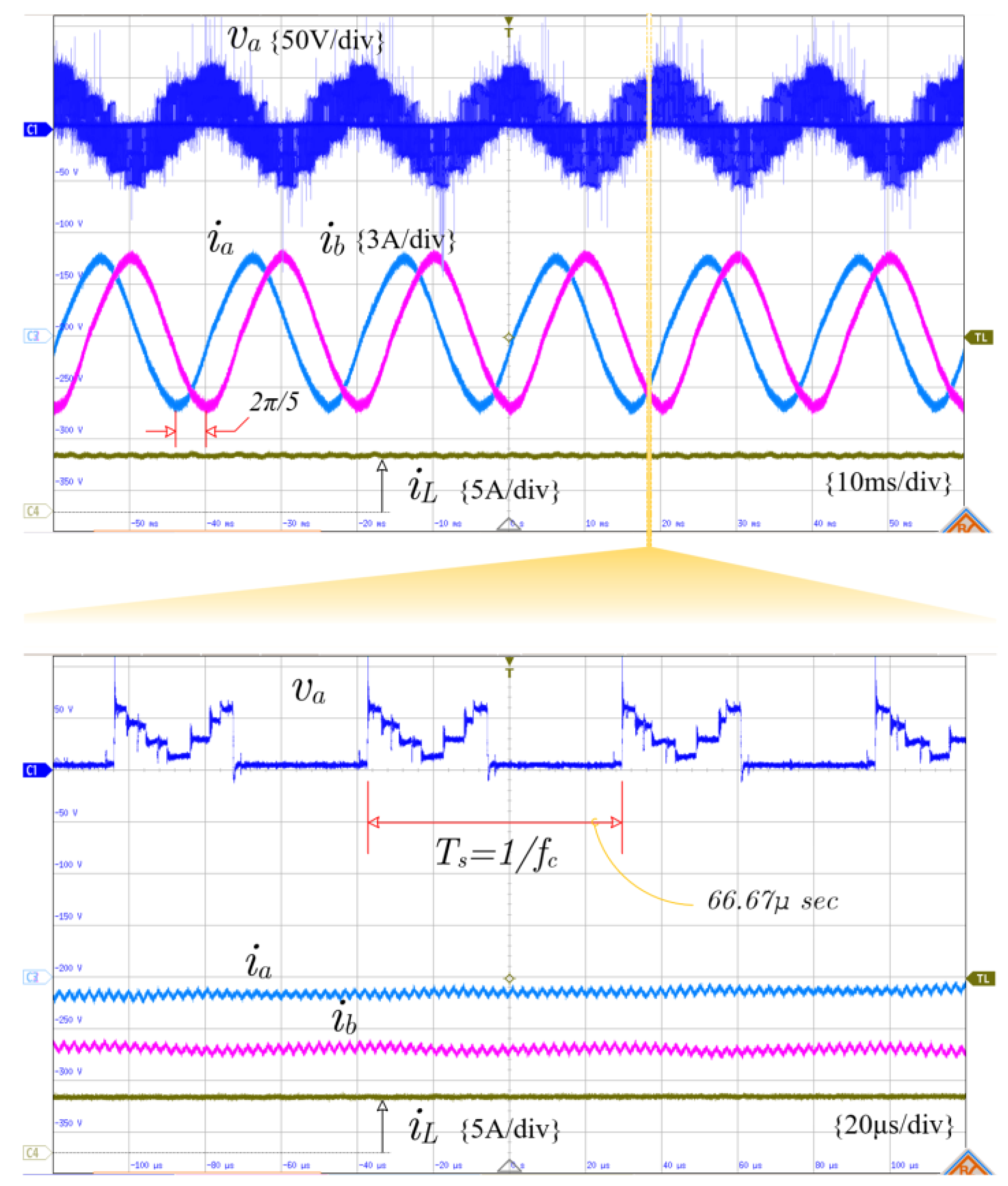
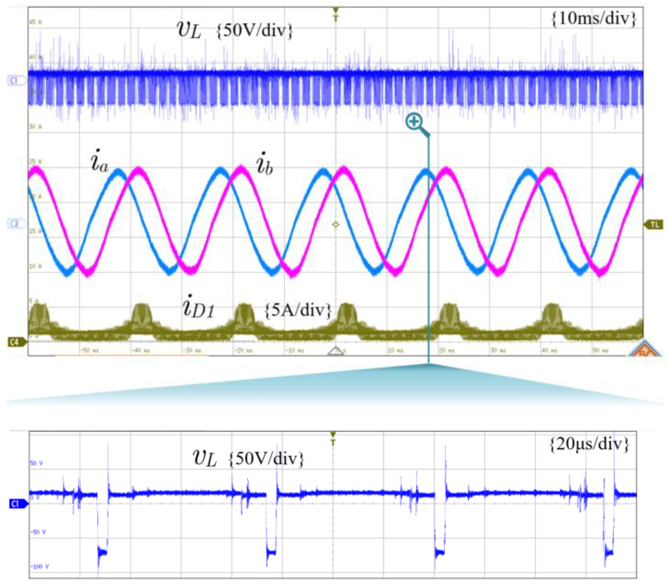
- Based on Figure 21, the waveforms of the output currents are near sinusoidal waveforms with low distortion and displaced by 2π/5. These results are close to the simulation results. As can be observed, the pulse width modulated output voltage is chopped according to the proposed scheme with a frequency, , of 15 kHz.
- From the inductor (supply) current waveform shown in Figure 21, it is worth noting that the inductor current is free from the low-order harmonics with the proposed PWM scheme. This is owed to utilizing fixed charging and discharging duty cycles in the proposed MSVM scheme. As you can see, the inductor current is continuous, with an average value of 5.3 A.
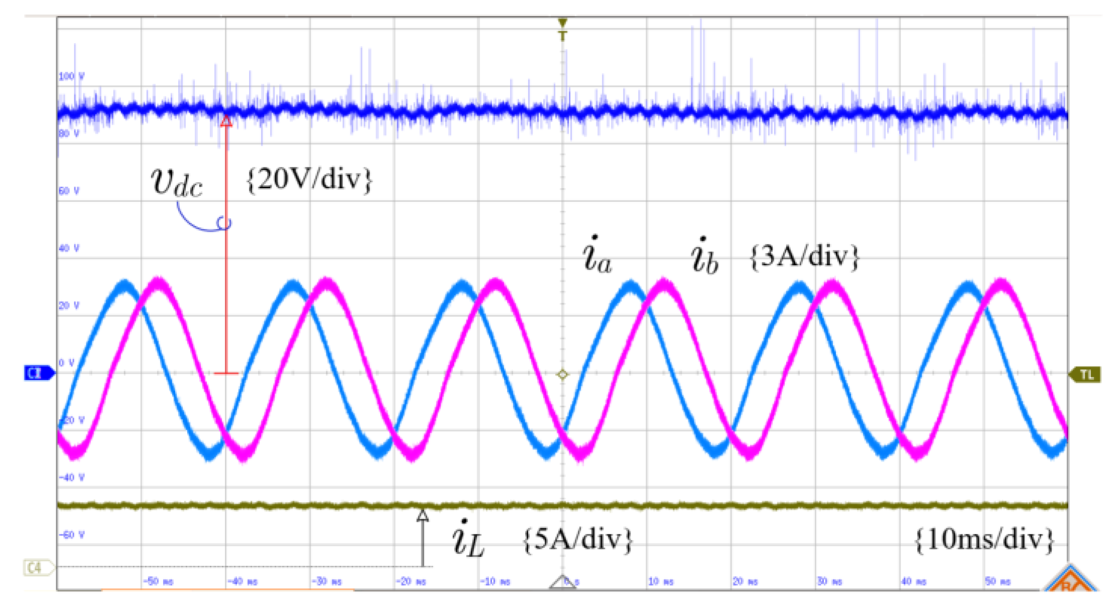
- The measured average voltage at the DC link from Figure 22 is 89 V. It agrees with the simulation and the mathematical analysis.
- Moreover, it can be observed from Figure 23 that the average voltage across the inductor is zero due, which proves the volt-second balance concept.
7. Conclusions
- (a)
- It has a continuous input current free of low-order harmonics;
- (b)
- The AC-output ripple is like that of the conventional space vector modulated five-phase VSIs; therefore, these ripples are smaller than those of Z-source inverters.
- (c)
- The boosting action is performed in a single stage, with fewer passive elements than Z-source inverters and without active switches as in two-stage inverters.
- (d)
- In addition, it uses the same standard modulation schemes as the five-phase inverter and there is no need for additional shoot-through pulses.
Author Contributions
Funding
Institutional Review Board Statement
Informed Consent Statement
Data Availability Statement
Conflicts of Interest
References
- Kindl, V.; Cermak, R.; Ferkova, Z.; Skala, B. Review of Time and Space Harmonics in Multi-Phase Induction Machine. Energies 2020, 13, 496. [Google Scholar] [CrossRef] [Green Version]
- Laksar, J.; Cermak, R.; Hruska, K. Challenges in the Electromagnetic Design of Multiphase Machines: Winding and Equivalent Circuit Parameters. Energies 2021, 14, 7335. [Google Scholar] [CrossRef]
- Dabour, S.M.; Rashad, E.M.; Abdel-khalik, A.; Ahmed, S.; Massoud, A. A new fifteen-switch inverter topology for two five-phase motors drive. In Proceedings of the 2016 Eighteenth International Middle East Power Systems Conference (MEPCON), Cairo, Egypt, 27–29 December 2016; pp. 729–734. [Google Scholar] [CrossRef]
- Dabour, S.M.; Abdel-Khalik, A.S.; Massoud, A.M.; Ahmed, S. Analysis of Scalar PWM Approach With Optimal Common-Mode Voltage Reduction Technique for Five-Phase Inverters. IEEE J. Emerg. Sel. Top. Power Electron. 2019, 7, 1854–1871. [Google Scholar] [CrossRef] [Green Version]
- Elgenedy, M.A.; Elserougi, A.A.; Abdel-Khalik, A.S.; Massoud, A.M.; Ahmed, S. A Space Vector PWM Scheme for Five-Phase Current-Source Converters. IEEE Trans. Ind. Electron. 2016, 63, 562–573. [Google Scholar] [CrossRef]
- Dabour, S.M.; Abdel-Khalik, A.; Ahmed, S.; Massoud, A. Performance of a three-to-five matrix converter fed five-phase induction motor under open-circuit switch faults. In Proceedings of the ISCAIE, Penang, Malaysia, 30–31 May 2016; pp. 159–164. [Google Scholar]
- Ellabban, O.; Abu-Rub, H. Field-oriented control of a five-phase induction motor fey by a Z-source inverter. In Proceedings of the 2013 IEEE International Conference on Industrial Technology (ICIT), Cape Town, South Africa, 25–28 February 2013; pp. 1624–1629. [Google Scholar] [CrossRef]
- Abduallah, A.A.; Iqbal, A.; Meraj, M.; Ben-Brahim, L.; Alammari, R.; Abu-Rub, H. Discontinuous space vector pulse width modulation techniques for a five-phase quasi Z-source inverter. In Proceedings of the IECON 2015-41st Annual Conference of the IEEE Industrial Electronics Society, Yokohama, Japan, 9–12 November 2015; pp. 004205–004210. [Google Scholar] [CrossRef]
- Ellabban, O.; Abu-Rub, H. Z-Source Inverter: Topology Improvements Review. IEEE Ind. Electron. Mag. 2016, 10, 6–24. [Google Scholar] [CrossRef]
- Kavya Santhoshi, B.; Mohana Sundaram, K.; Padmanaban, S.; Holm-Nielsen, J.B. Critical Review of PV Grid-Tied Inverters. Energies 2019, 12, 1921. [Google Scholar] [CrossRef] [Green Version]
- Abdelhakim, A.; Blaabjerg, F.; Mattavelli, P. Modulation Schemes of the Three-Phase Impedance Source Inverters—Part I: Classification and Review. IEEE Trans. Ind. Electron. 2018, 65, 6309–6320. [Google Scholar] [CrossRef]
- Yuan, J.; Yang, Y.; Blaabjerg, F. A Switched Quasi-Z-Source Inverter with Continuous Input Currents. Energies 2020, 13, 1390. [Google Scholar] [CrossRef] [Green Version]
- Yi, F.; Cai, W. A Quasi-Z-Source Integrated Multiport Power Converter as Switched Reluctance Motor Drives for Capacitance Reduction and Wide-Speed-Range Operation. IEEE Trans. Power Electron. 2016, 31, 7661–7676. [Google Scholar] [CrossRef]
- Dabour, S.M.; Abdel-Khalik, A.S.; Ahmed, S.; Massoud, A.M. A Family of Discontinuous PWM Strategies for Quasi Z-Source Nine-Switch Inverters. IEEE Access 2021, 9, 169161–169176. [Google Scholar] [CrossRef]
- Ribeiro, H.; Pinto, A.; Borges, B. Single-stage DC-AC converter for photovoltaic systems. In Proceedings of the IEEE Energy Conversion Congress and Exposition, Atlanta, GA, USA, 12–16 September 2010; pp. 604–610. [Google Scholar]
- Abdelhakim, A.; Mattavelli, P.; Spiazzi, G. Three-Phase Split-Source Inverter (SSI): Analysis and Modulation. IEEE Trans. Power Electron. 2016, 31, 7451–7461. [Google Scholar] [CrossRef]
- Akbar, F.; Cha, H.; Ahmed, H.F.; Khan, A.A. A Family of Single-Stage High-Gain Dual-Buck Split-Source Inverters. IEEE J. Emerg. Sel. Top. Power Electron. 2020, 8, 1701–1713. [Google Scholar] [CrossRef]
- Chen, M.; Yin, C.; Loh, P.C. Magnetically Coupled High-Voltage-Boost Split Y-Source Inverter Without Leakage-Induced Voltage Spikes. IEEE Trans. Ind. Electron. 2020, 67, 5444–5455. [Google Scholar] [CrossRef]
- Dabour, S.M.; Alotaibi, M.A.; Abd-Elaziz, A.A.; Alshahat, M.A.; Abdallah, M.; Eltamaly, A.M.; Abdel-Khalik, A.S.; Massoud, A.M.; Ahmed, S. Modeling and Control of Single-Stage Quadratic-Boost Split Source Inverters. IEEE Access 2022, 10, 24162–24180. [Google Scholar] [CrossRef]
- AbdulSalam, M.; Dabour, S.M.; Rashad, E.M. Cascaded Multilevel Split-Source Inverters: Analysis and Modulation. In Proceedings of the 2019 21st International Middle East Power Systems Conference (MEPCON), Cairo, Egypt, 17–19 December 2019; pp. 1204–1209. [Google Scholar] [CrossRef]
- Montazeri, S.H.; Milimonfared, J.; Zolghadri, M. A New Modeling and Control Scheme for Cascaded Split-Source Converter Cells. IEEE Trans. Ind. Electron. 2022, 69, 7618–7628. [Google Scholar] [CrossRef]
- Montazeri, S.H.; Milimonfared, J.; Zolghadri, M.R. Multidimensional Pulsewidth Modulation for Cascaded Split-Source Inverter. IEEE Trans. Ind. Electron. 2023, 70, 137–146. [Google Scholar] [CrossRef]
- Dabour, S.M.; Abdel-Khalik, A.S.; Ahmed, S.; Massoud, A. An Optimal PWM Technique for Dual-Output Nine-Switch Boost Inverters With Minimum Passive Component Count. IEEE Trans. Power Electron. 2021, 36, 1065–1079. [Google Scholar] [CrossRef]
- Pinjala, M.K.; Bhimasingu, R. Improving the DC-Link Utilization of Nine-Switch Boost Inverter Suitable for Six-Phase Induction Motor. IEEE Trans. Transp. Electrif. 2020, 6, 1177–1187. [Google Scholar] [CrossRef]
- Abdelhakim, A.; Mattavelli, P.; Boscaino, V.; Lullo, G. Decoupled Control Scheme of Grid-Connected Split-Source Inverters. IEEE Trans. Ind. Electron. 2017, 64, 6202–6211. [Google Scholar] [CrossRef]
- Dabour, S.M.; Aboushady, A.A.; Elgenedy, M.A.; Gowaid, I.A.; Farrag, M.E. Current Ripple Evaluation of Space Vector Modulated Five-Phase Split-Source Inverters. In Proceedings of the 2022 57th International Universities Power Engineering Conference (UPEC), Istanbul, Turky, 30 August–2 September; pp. 1–6. [CrossRef]
- Dujic, D.; Jones, M.; Levi, E. Analysis of Output Current Ripple RMS in Multiphase Drives Using Space Vector Approach. IEEE Trans. Power Electron. 2009, 24, 1926–1938. [Google Scholar] [CrossRef]
- Rohde & Schwarz R&S®RTM3000 Oscilloscope. Available online: https://www.rohde-schwarz.com/uk/products/test-andmeasurement/oscilloscopes/rs-rtm3000-oscilloscope_63493-427459.html (accessed on 10 October 2021).


| Parameters | Values | Parameters | Values |
|---|---|---|---|
| Input voltage | 45 V | Input inductance | 1.28 mH |
| DC-link capacitor | 480 μF | RL-load | 4.7 Ω, 5 mH |
| Modulation index | 0.5 | Switching frequency | 15 kHz |
Publisher’s Note: MDPI stays neutral with regard to jurisdictional claims in published maps and institutional affiliations. |
© 2022 by the authors. Licensee MDPI, Basel, Switzerland. This article is an open access article distributed under the terms and conditions of the Creative Commons Attribution (CC BY) license (https://creativecommons.org/licenses/by/4.0/).
Share and Cite
Dabour, S.M.; Aboushady, A.A.; Gowaid, I.A.; Elgenedy, M.A.; Farrag, M.E. Performance Analysis and Evaluation of Multiphase Split-Source Inverters. Energies 2022, 15, 8411. https://doi.org/10.3390/en15228411
Dabour SM, Aboushady AA, Gowaid IA, Elgenedy MA, Farrag ME. Performance Analysis and Evaluation of Multiphase Split-Source Inverters. Energies. 2022; 15(22):8411. https://doi.org/10.3390/en15228411
Chicago/Turabian StyleDabour, Sherif M., Ahmed A. Aboushady, I. A. Gowaid, Mohamed. A. Elgenedy, and Mohamed E. Farrag. 2022. "Performance Analysis and Evaluation of Multiphase Split-Source Inverters" Energies 15, no. 22: 8411. https://doi.org/10.3390/en15228411