
DC-DC High-Step-Up Quasi-Resonant Converter to Drive Acoustic Transmitters


1
College of Science and Engineering, Flinders University, Adelaide 5042, Australia
2
STEM, University of South Australia, Adelaide 5001, Australia
3
Research and Development Department, Eram Sanat Mooj Gostar Company, Shiraz 71976-87811, Iran
*
Authors to whom correspondence should be addressed.
Energies 2022, 15(15), 5745; https://doi.org/10.3390/en15155745
Submission received: 8 July 2022
/
Revised: 2 August 2022
/
Accepted: 6 August 2022
/
Published: 8 August 2022
(This article belongs to the Topic Power Converters)
Abstract
:This paper proposes a quasi-resonant step-up DC-DC converter to provide the DC-link voltage for piezoelectric transmitters (PZETs). The resonance not only provides a soft-switching condition for the converter switches, but also helps to decrease the converter element sizes for marine applications. Operation modes of the proposed converter are discussed. The current and voltage of the converter components are derived analytically, and hence the converter gain is obtained. The performance of the proposed high-step-up, high-power density converter is examined through a comprehensive simulation study. The simulation results demonstrate the soft-switching operation and short transient time required for the converter to reach the reference output voltage. The converter output voltage remains unchanged when an inverter with a passive filter is placed at its output while supplying the PZET. The proposed DC-DC converter is prototyped to validate the converter gain and soft-switching operation experimentally. The converter gain and soft-switching results in simulation are well matched with those of the experimental tests. The converter efficiency in three different switching frequencies is obtained experimentally. The power density of the proposed topology is determined via the designing of a printed circuit board. The experimental results demonstrate the appropriate gain and efficiency of the converter in the tested power range.
1. Introduction
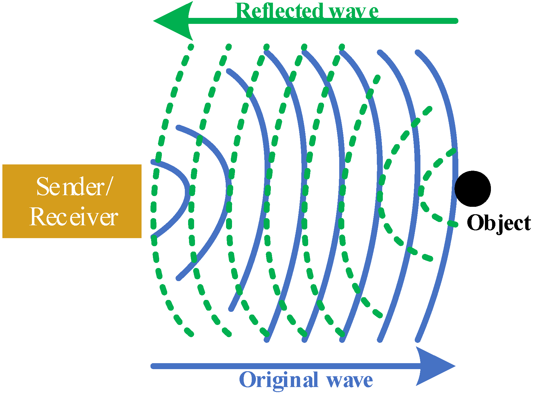
Acoustic transmitters have a significant role in the provision of a safe maritime trip. These transmitters use sound navigation and ranging (SONAR) technique to detect the seabed, near species, and possible obstacles during a voyage [1,2]. In addition, these waves warn the available fishes, whales, and all other living animals to move away from the moving vessels [3]. SONAR systems usually generate sound waves over a course of time, called pinging, and then stop generation to receive the reflected waves from the seabed and available obstacles [4]. Figure 1 shows the transmitting and receiving waves between the underwater transmitter and a sample object. In this regard, piezoelectric materials that can work in two operating areas (i.e., generating and motoring modes) are employed for pinging and receiving waves. The piezoelectric materials generate underwater sound during the motoring period when energized via an alternative current (AC) power supply. Piezoelectrics receive the reflected sounds when the energization time is concluded. In fact, they generate a low voltage power because of the received energy.
Piezoelectric transmitters (PZETs) require a high voltage level to work in motoring mode [5]. However, the available power source in ships and submarines, where the PZETs are located, is usually limited to a low-voltage battery package. It must be noted that the required voltage level for PZETs varies from 50 to 1000 volts, based on the operation of PZETs at different sea depths. If the applied voltage to the PZET is set to a higher level as required in the lower depths of the sea, the piezoelectric element will be consequently broken. Thus, a high-step-up power converter is needed to provide the precise voltage level for driving the PZET [6]. The availability of only a small space to place the transmitters and their power supply restricts the utilization of low-power-density converters for PZETs [7]. These converters are placed in harsh and noisy environments. Therefore, an analog robust controller is preferred instead of the digital controllers.
Designers mostly used class A, B, and AB linear power amplifiers to supply PZETs [8]. The low efficiency of linear amplifiers not only demands large heat sinks because of the generation of the unwanted heat [9], but also increases the required size of the power source (e.g., battery packages). The gain of a class AB was enhanced by a class D switching in [10]. However, such a linear amplifier still suffers from low efficiency and large volume. Switching power converters are suitable substitutions for the linear power converters because of their higher power density and efficiency.
The DC-DC switching power converters are categorized into isolated and non-isolated families [11,12,13]. The isolated converters, which benefit from the availability of high-frequency transformers in their structures, provide an intrinsic input–output insulation [14]. The insulation is required in some high-power applications where engineers need to decrease the electric shocks of each side of the power supply [15]. For instance, it provides a layer of insulation in grid-tied converters [16]. However, they have a lower power density and efficiency compared to non-isolated power converters. Moreover, the isolation complicates the implementation of the control system. Thus, the non-isolated power supplies are more popular, especially in low-power applications [17].
Usually, non-isolated converters employ coupled inductors or resonance phenomena to reach a higher output voltage [18]. Switching power supplies equipped with coupled inductors have lower power densities due to the bulky components (e.g., inductors and capacitors) available in their structure [19,20]. Hence, a resonant power converter can be used in an application where the power density is a significant factor [21]. The resonance frequency in these types of converters is higher than the switching frequency, which leads to a reduction in the converter elements’ size. Although the energy conversion through resonance creates higher voltage and current stress, it provides a higher gain for a converter. Therefore, the resonance-based converters have a higher gain and power density in comparison to other types of non-isolated converters [22]. Moreover, the lack of an isolating high-frequency transformer enables them to have higher efficiency compared to isolated converters.
Zero-voltage and current-switching strategies are two advanced switching methods of decreasing the switching losses of a converter and helping switches to work in their safe operating areas (SOAs). The conventional resistive-capacitive snubber was the earlier method of providing ZVS and ZCS for the switches of a converter [23]. The resistance of such topologies reduces the converter efficiency. Hence, the active-clamped circuits [24] and resonant snubbers [25] are more popular among engineers because of their lossless characteristic. The resonant-based power converters have a natural soft switching, which helps them to protect their components and gives them a high efficiency [26].
Although the literature does not consider the resonant converter as an interface circuit for PZETs, it seems logical to use the resonance phenomena in a PZET drive system to provide the DC voltage. It is obvious that the converter operating at a higher frequency requires smaller components, and is consequently a high-power density converter. Furthermore, the resonance not only assists in increasing the converter gain, but also provides the soft-switching condition for the converter switches. Therefore, the converter efficiency is increased because of the soft switching.
Usually, PZETs are energized over a small time span and receive the echo sounds over a greater time span [27]. Under this condition, the response time of the power supply is pivotal in the energization of the PZETs. Due to the resonance, the proposed converter operates rapidly enough to reach the required output voltage. As a non-isolated converter, the control system of the converter has much lower complexity than an isolated converter. It was also demonstrated that the proposed converter has a power density and gain comparable to previously introduced converters in literature.
Commercialized power supplies have a limited range of output voltage [28]. Hence, they are not suitable to be used as drivers of PZETs transmitters requiring a wide range of DC volage [5]. Furthermore, most commercialized converters have an isolated topology, complicating the implementation of the control system (i.e., provision of the feedback signal). The literature has introduced different topologies of high-step-up DC-DC converters for different applications [29,30,31]. However, they cannot operate in a wide range of duty cycles. It was shown that the proposed converter of this study not only offers the required gain over a wider range of duty cycles, but also has a higher power density as compared to those of commercially available converters. From the scientific point of view, the topology of the converter is new, and it offers comparable performance parameters as compared to the previously introduced converters discussed in literature [32,33,34,35]. In addition to the new topology, the mathematical model of the converter is provided, facilitating understanding of the converter’s behavior.
The proposed converter operation modes and its mathematical modeling are described in Section 2. The design procedure is described at the end of this section. A 120 W converter is designed in the third section, and its performance is analyzed using the simulation analysis to validate the presented theory. The converter is prototyped to validate the circuit. The experimental results are presented in Section 4.
2. Proposed DC-DC Power Converter
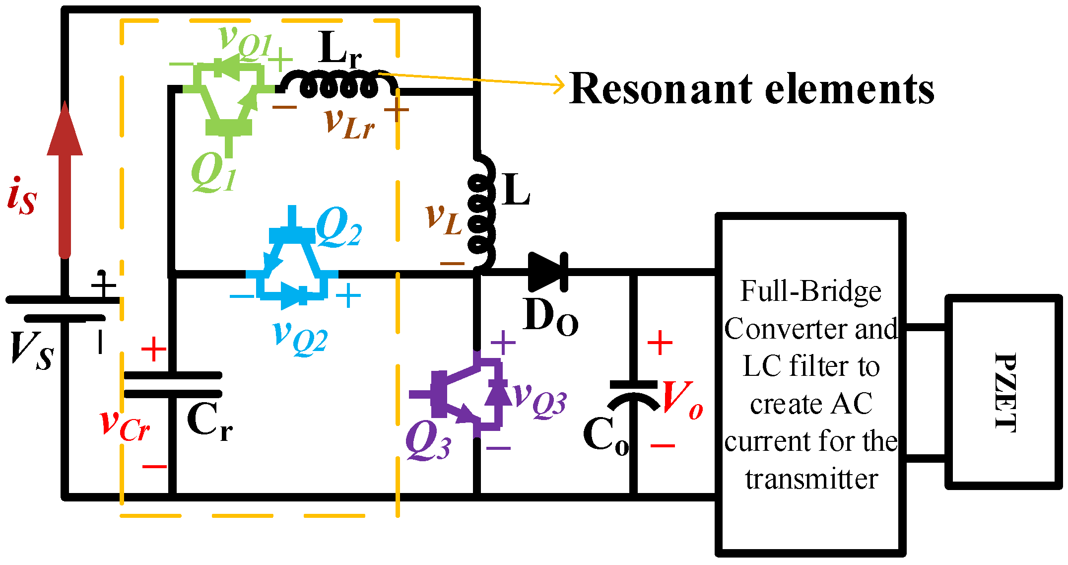
A resonance circuit consisting of an inductor, a capacitor, and two power switches was added to the basic structure of the conventional boost converter to create the proposed converter (see Figure 2). AC voltages with high total harmonic distortion reduce PZET lifetime and lead to the breakage of PZETs. Thus, PZETs must be supplied by a semi-sinusoidal voltage to work safely. A package consisting of an H-bridge converter and LC filter was at the end of the proposed DC-DC converter to provide the required PZET voltage. In other words, the sharp edges of a rectangular pulse were obviated using the designed LC filter to protect the PZET. The converter switching strategy and the energy conversion through the resonance, which are explained in the next part, had crucial roles in the correct performance of the converter.
In this section, the ESR of the capacitor and resistance of the inductor are disregarded for the modeling and analysis. Additionally, it is assumed that the converter is supplied with a lossless battery package. The rising and falling time of the diode and switch conduction time are disregarded.
2.1. Converter Operation
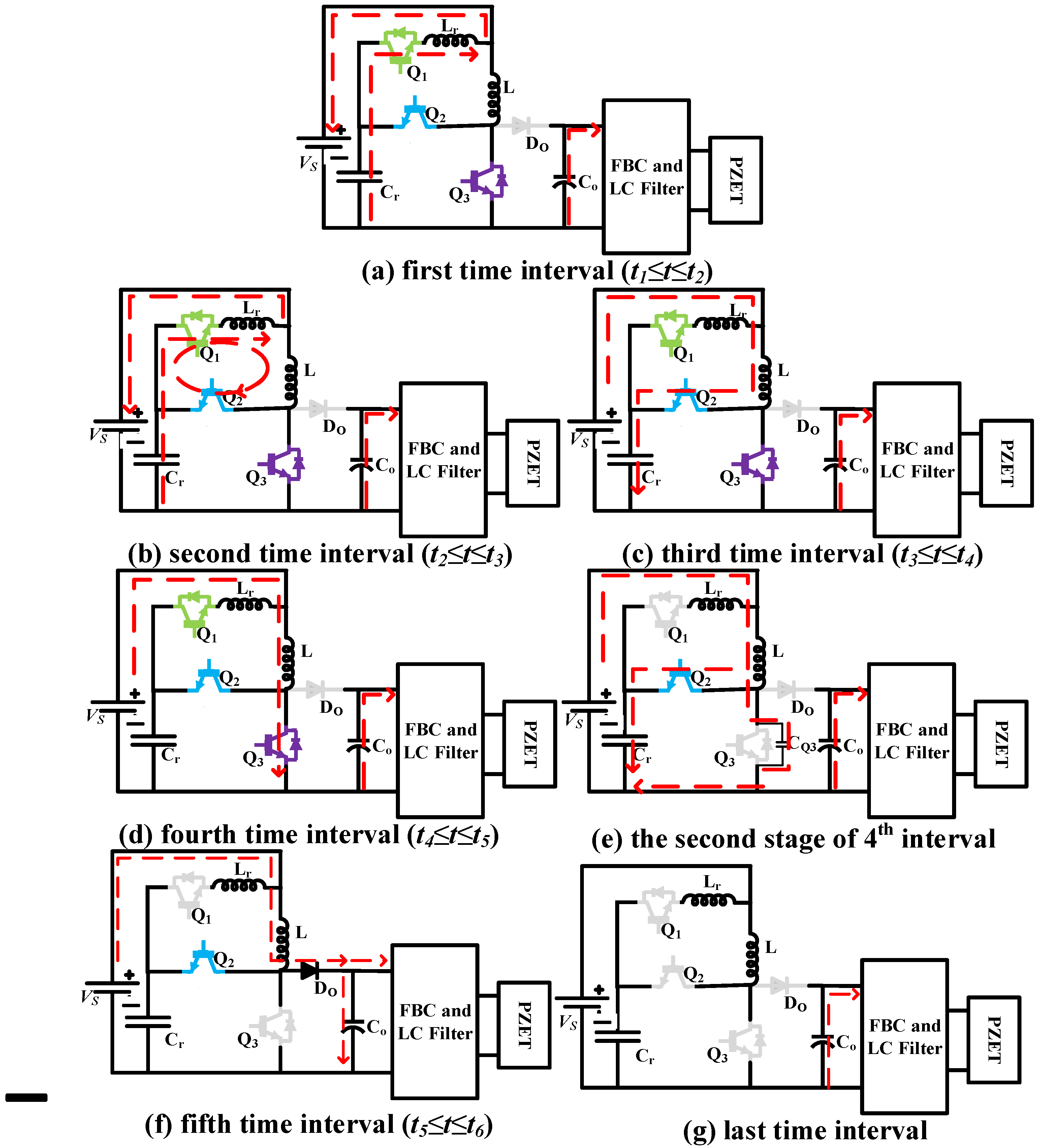
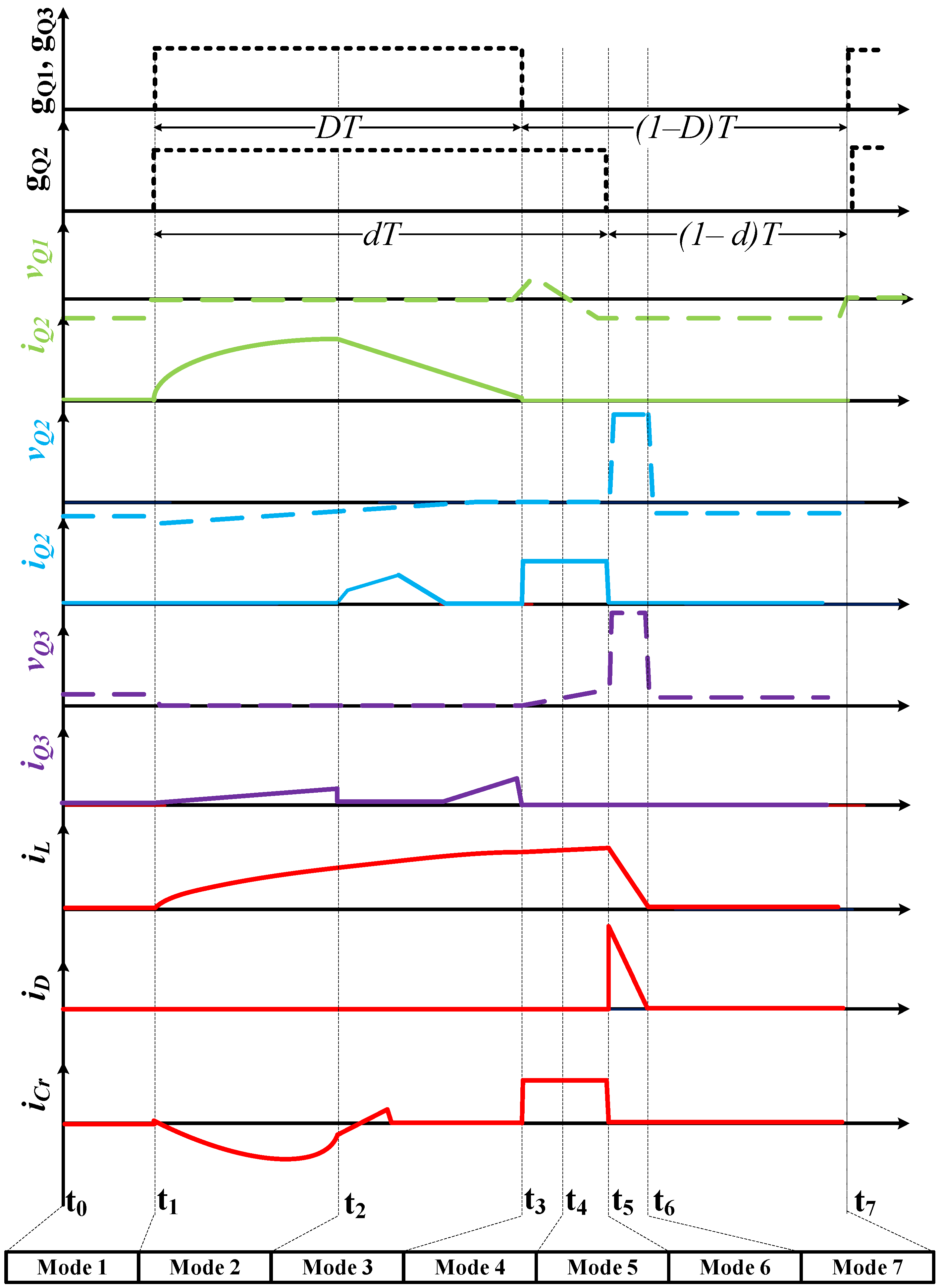
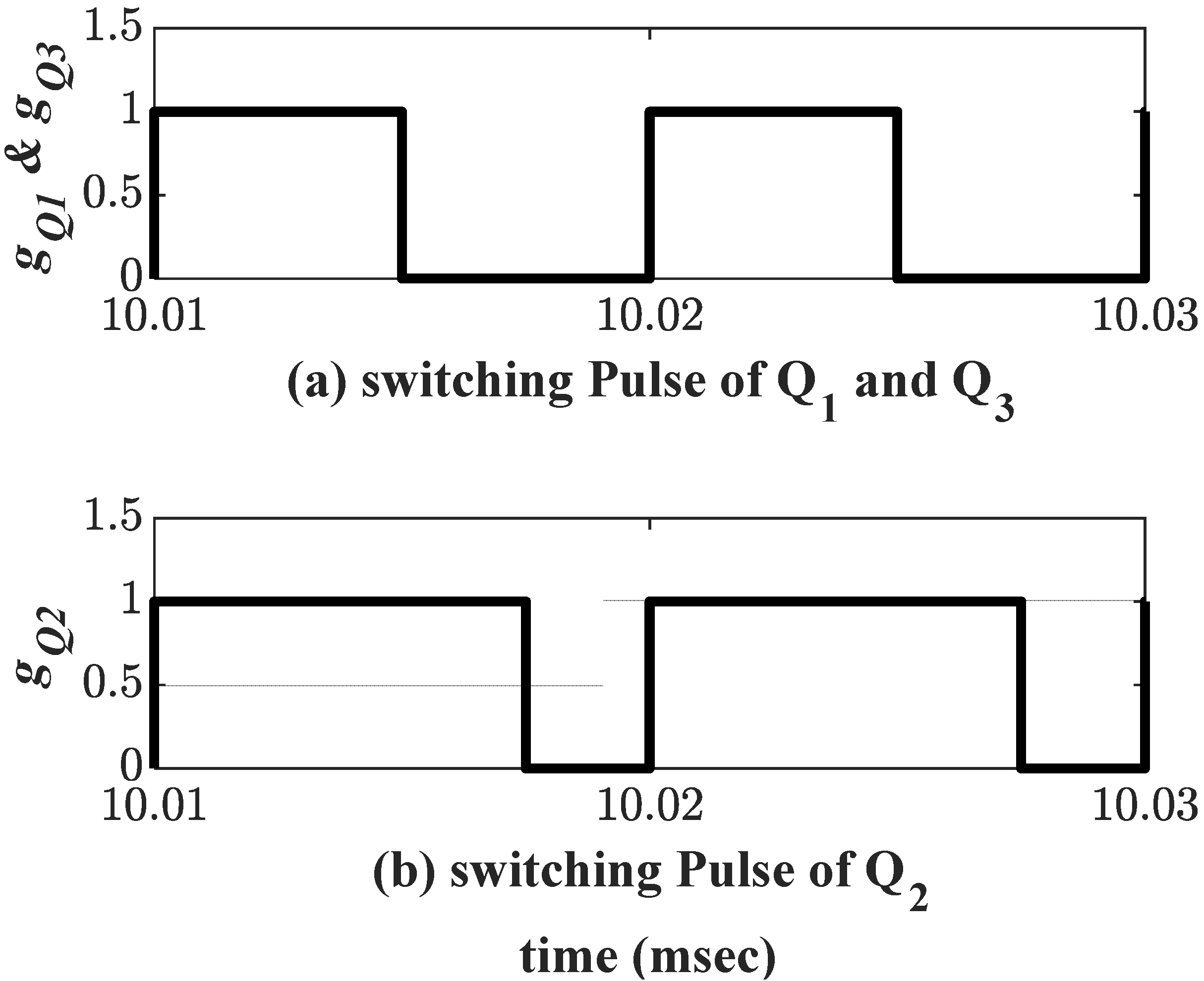
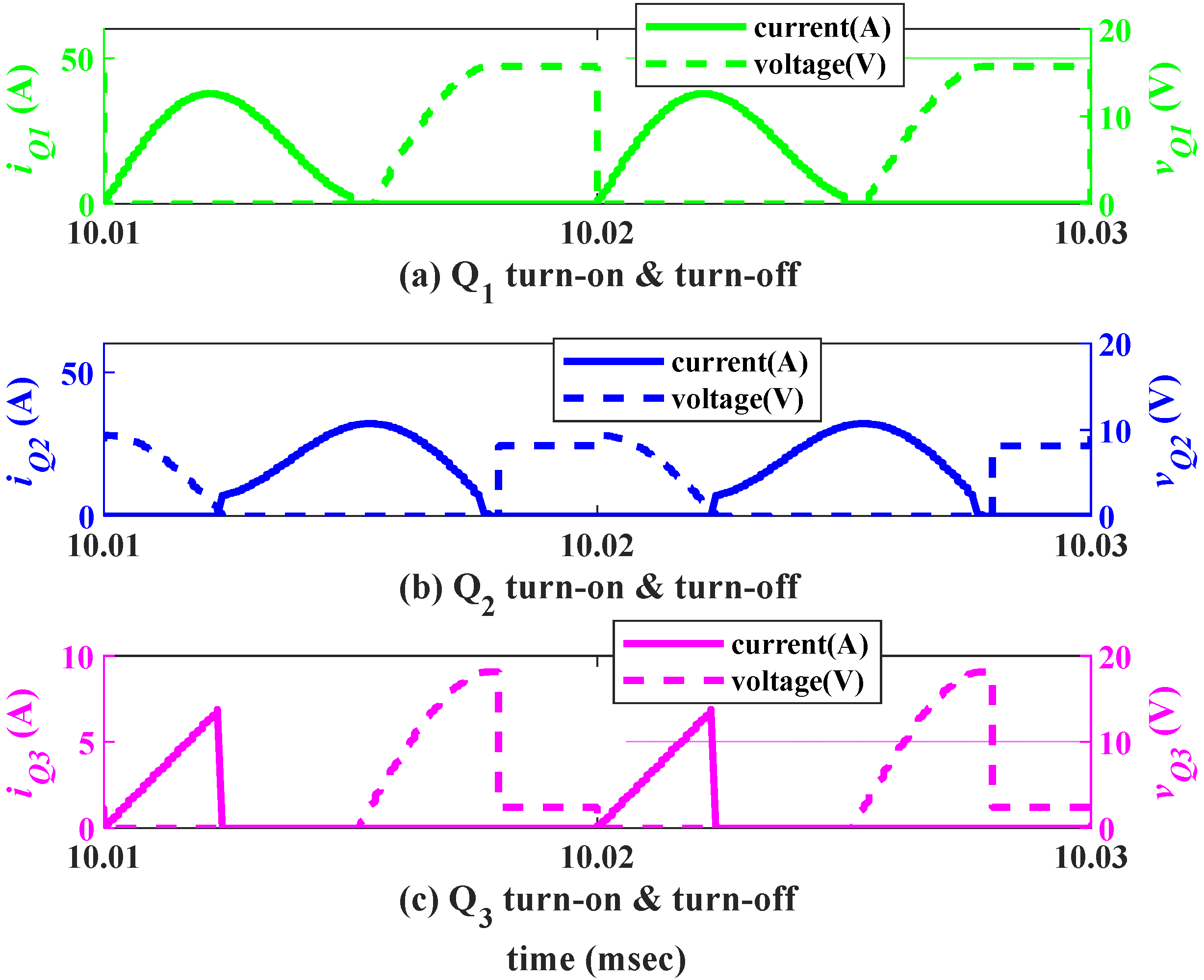
All operating modes of the proposed DC-DC converter shown in Figure 3 are discussed in this section. Several selective waveforms, presented in Figure 4, are used to explain the operation of the proposed converter clearly. According to these figures, VQ1, VQ2, and VQ3 represent the voltage of the converter switches, while IQk (k = 1, 2, 3) is the related switch current. The current of the resonance inductor (Lr) is equal to IQ1. According to Figure 4, the energy conversion period starts from t0 when all switches are off, and the load is supplied by the output capacitor. Note that the transient operation of the converter ends at t0, and it is the start of the steady-state operation.
In the steady-state operation of the converter, the resonance capacitor (Cr) has an initial charge (Vint) at t1, which is stored from the resonance of the main inductor (L) with Cr. Thus, Vint is significantly greater than the source voltage (VS). In the first time interval (t1 ≤ t ≤ t2), Q1 and Q3 are required to be turned on when the Cr initial voltage is greater than the source and the initial energy of both L and Lr is zero. According to Figure 3a, Cr depletes Lr through two different current paths, which charges L and the battery package. Because the source does not find time to energize the converter elements, both switches have time to start conduction in ZVS condition. Additionally, Q2 can be turned on in the zero current switching (ZCS) condition when Q3 is on, and Cr releases its energy. In this time interval, the power converter elements voltage and current vary based on the equations presented in (1):
where
In the second time interval (t2 ≤ t ≤ t3), when vCr accedes to zero, the stored energy in Lr circulates through L while depleting into the battery package (Figure 3b). This time interval is concluded when all Lr stored energy is delivered to L and the battery package. Note that Cr is negatively charged when Lr delivers energy to the battery package. At the end of this time interval, as shown in Figure 3c, a small amount of the stored energy in L is delivered to Cr to satisfy the charge balance of the capacitor. t2 can be easily derived from the resonance capacitor voltage equation in (1). The converter element energy conversion can be formulated as follows in this time interval:
The Lr current reaches zero at the end of this time interval. Then, t3, as presented in (4), is calculated by means of the ILr(t) equation from (3).
In the third time interval (t3 ≤ t ≤ t4), Q2 is on and vCr is zero. Q3 is already turned on in ZVS at t1, and its voltage is zero. Then, Q3 starts conduction in ZVS and L is charged by the input source (Figure 3d). This time interval is concluded when the turn-off gate commands are sent to Q1 and Q3. When the Q1 current and vCr are zero because of the previous energy conversion during previous intervals, Q1 and Q3 are turned-off in the ZCS and ZVS conditions, respectively. The main inductor current equation is written in (5).
The inductor current can be calculated by (5) where t4 = DT.
In the fourth time interval (t4 ≤ t ≤ t5), Q2 begins to conduct the input current in ZVS through a resonance between L and Cr. According to the Figure 3e, the parallel capacitor of Q3 is charged during the L and Cr resonance and its voltage is equal to vCr. Therefore, Q2 can be turned off in ZVS when the off command is sent to its gate. iL and vCr can be calculated by (7) in this time interval:
where
This interval is concluded when Q2 is turning-off at dT. The calculated value for vCr at t5 = dT is equal to Vint defined in (1).
The main inductor stored energy is delivered to load through the output diode (DO) at the fifth time interval presented in Figure 3f (t5 ≤ t ≤ t6). Note that the value of d, which determines Q2 operating time, plays a prominent role in the determination of the converter gain. According to Figure 4, d must be greater than D. Cr voltage reaches the output voltage after a quarter of the resonance, which leads to DO conduction. In this condition, DO will conduct current to load inherently, which will be the highest gain of the converter. Therefore, Q2 turn-off time must be smaller than a quarter of the resonance after Q1 and Q3 turn-off, where Q2 is used to control the gain. Where a quarter of the resonance is calculated by (10), dT can be at most 0.25T greater than DT.
Thus, 0.25T required time for maximum dT limits the maximum value of D to 0.75, which forces the proposed converter to work in discontinuous conduction mode (DCM) operation. Therefore, DCM operation is the appropriate mode for designing the value of converter elements.
In the last time interval, shown in Figure 3g, the output capacitor supplies the load with its stored energy.
The converter offers soft switching when the voltage second balance of the inductors and current balance of the capacitors are provided. According to (10), a quarter of the resonance should be completed to achieve this voltage and current balances in inductor and capacitors. Thus, the maximum duty cycle is 0.75. Additionally, a quarter of the resonance is required to charge the inductor Lr up to its peak current. Therefore, the minimum possible duty cycle for permeation of the soft switching is 0.25 if the switching frequency is set to be equal to the resonance frequency. The minimum value of the duty cycle can be reduced by increments in the switching frequency. For instance, the minimum duty cycle is 0.2 when switching frequency and resonance frequency are 100 kHz and 120 kHz.
2.2. Converter Gain
The converter gain is obtained using the voltage-balance equation of the main inductor presented in (11a). In (11a), inductance coefficient () is simplified from two sides of the equality. Then, the integral terms should be calculated to find the converter gain. The simplified term is shown in (11b):
where vCr is the resonance capacitor voltage equation presented in (7) and t5 is equal to dT. The second term of the left side of (11b) is found by (12).
If the converter works in the boundary of DCM operation, DO must conduct the main inductor current utmost until t6 = T. Thus, the load will be energized by input source and L from dT to the end of the period (T). In this condition, the right side of (11) is calculated as follows:
Considering (11)–(13), the converter gain, which depends on the switching frequency, is calculated by (14).
2.3. Design Procedure
The design of the converter power components starts with the design of the main inductor. The value of the obtained inductor is used to find the resonance capacitor () based on the resonance, which occurs between these two elements in the fourth interval of energy conversion. The resonance inductor is obtained by consideration of the resonance happening between the and through the first interval of the energy conversion.
The voltage equation of the main inductor (L), when Q3 is on, is used to calculate the value of the inductor as below:
where ΔIL is the maximum value of the inductor current. The ΔIL value, which can be determined by the input and output power relationship presented in (16), is required to continue the calculation.
The average of the input current Iin must be equal to the average of the inductor current within a period to ensure the voltage-second balance of the inductor. The maximum value of ΔIL is calculated at the DCM boundary. Figure 5 shows the main inductance current (IL) and the battery current (Iin) at the DCM boundary. As demonstrated in (17), the maximum value of ΔIL will be twice the average of input current.
Therefore, the maximum of ΔIL is computed by (18) where Iin is replaced by its calculated value from (16):
where PO is the maximum output power. The voltage-second balance of L must be satisfied when the converter works on its maximum duty cycle (Dmax). Therefore, D in (15) must be equal to the maximum required duty cycle, which can be derived from (14). For a certain converter, the ratio of over is given by the user. Thus, the maximum value of D using (14) is obtained when the maximum value of d (i.e., maximum dT = 0.25 T) is assumed at the DCM boundary. Consideration of Dmax and substitution of the calculated ΔIL in (15) results in L, as below:
Since the main inductance must be in resonance with Cr within a specific time interval, Cr can be calculated based on the switching frequency, as follows:
The resonance frequency of Lr with Cr is greater than the switching frequency, which is shown by fr. When fr is assumed by a designer, the value of Lr is calculated by (21).
The value of the output capacitor is determined in the last section of the design procedure. It is obvious that the output capacitor (CO) must supply the load when energy conversion among the elements does not let the battery package supply the load. Therefore, the worst condition occurs in the maximum duty cycle when the maximum output current is obtained from CO. According to the relationship of the capacitor voltage and current, CO capacity can be calculated by (22):
where ΔVO represents the maximum allowable output voltage level. In the next section, a simulation study is carried out to examine the performance of the proposed power converter.
3. Simulation Study
3.1. PZET Operation
PZETs must be supplied in their resonance frequency within a period to transmit data. After that, the power supply stops working, and the PZETs receive the reflected acoustic waves. For instance, a special PZET with the impedance of Z = 330 − 19° was studied in [6], requiring an AC voltage with 40 kHz frequency within 15 milliseconds to send data. After this operating period, the supply was disconnected and the PZET needed 2 s to receive the reflected wave from the underwater objects. It is assumed that the proposed converter drives the aforementioned PZET in this simulation study.
3.2. Design of the Converter Elements
In this study, the converter was designed based on the maximum allowable duty cycle (Dmax = 0.75) to examine the converter performance in all duty cycles. Additionally, it is supposed that the switching frequency (fsw) and resonance frequency (fr) are 100 kHz and 120 kHz, respectively. Therefore, the L value calculated by (19) is 0.86 μH, where the PZET consumes 100 W power in the maximum duty cycle and the converter is supplied by 2.4 volts rechargeable battery package. In this condition, Cr and Lr values extracted from (20) and (21) based on the obtained L are equal to Cr = 3.3 μF and Lr = 0.57 μH, respectively. Finally, the output capacitor of 1.2 μF is obtained by (22) when a 5-volt voltage ripple is considered as the applied restriction for ΔVO.
Table 1, which compares the proposed converter elements’ sizes with four other previously proposed high-step-up high-efficiency converters in an approximately equal power range, demonstrates the high-power density of the proposed converter. This table also shows the capability of the converter for operation over a wider/comparable range of duty cycles, allowing more flexibility to achieve different voltage levels.
Most of the commercialized converters include a high-frequency transformer, which leads to the isolation of input/output [28]. The transformer availability complicates the control system and increases the power density of the system. Furthermore, the output voltage range becomes limited to a smaller range. For instance, an H-bridge converter can only operate in smaller duty cycles in the range of 0.1–0.4.
3.3. Simulation Results
The simulation was run to validate the soft-switching operation of the proposed converter switches and its gain in the presence of a PIEZO-electric load model with impedance of Z = 330 − 19° .
The simulation was executed when the converter switches were commanded with a 50% duty cycle in 100 kHz operation frequency shown in Figure 6. Figure 7 shows the ZVS and ZCS operation of the proposed converter switches in a period when the considered gate commands were applied to them. The soft switching not only reduced the switching losses of the converter but also facilitated the operation of the SOA.
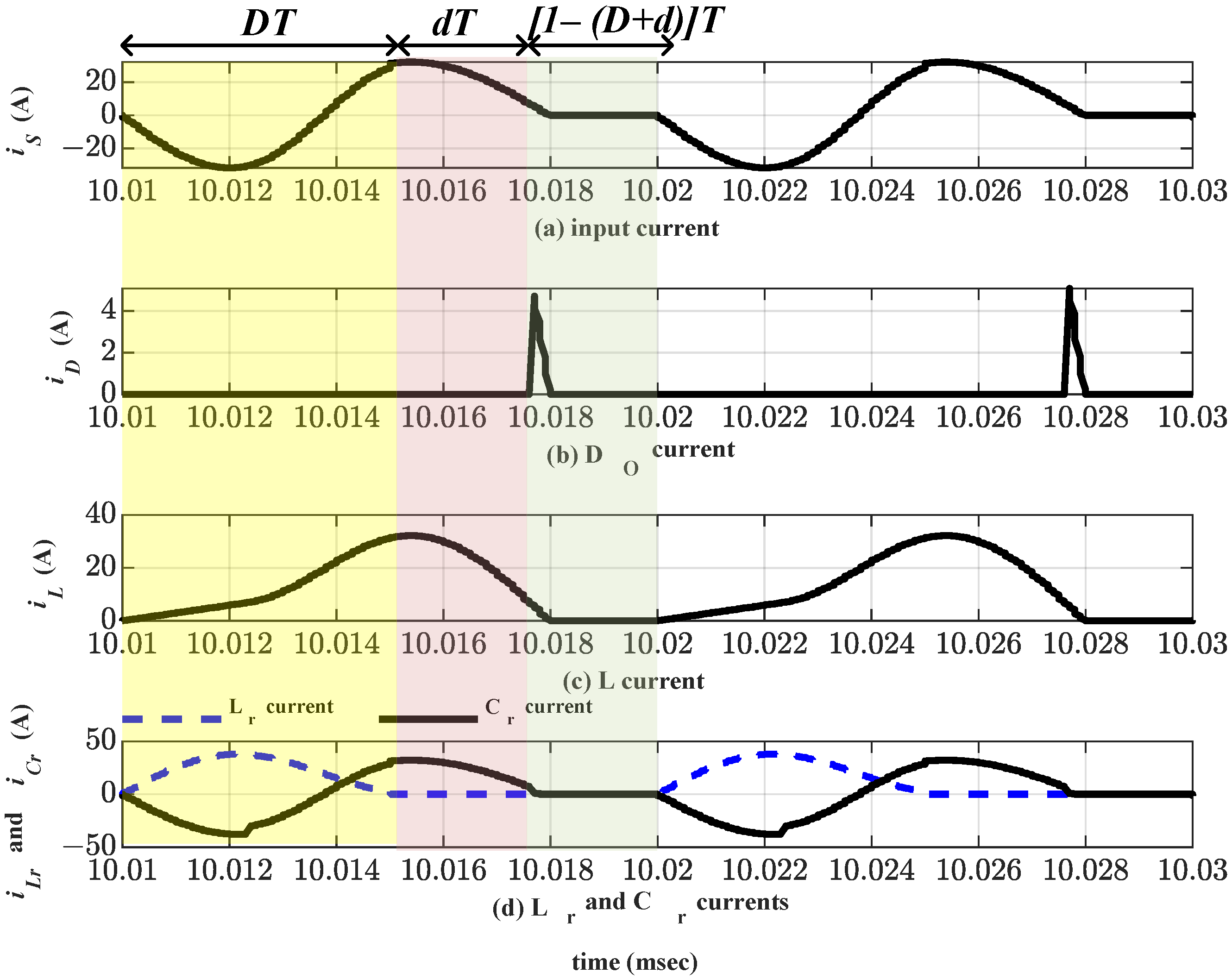
The input current, diode current, and current variation of the resonance elements in three switching periods are shown in Figure 8 to show the energy swing among the converter elements.
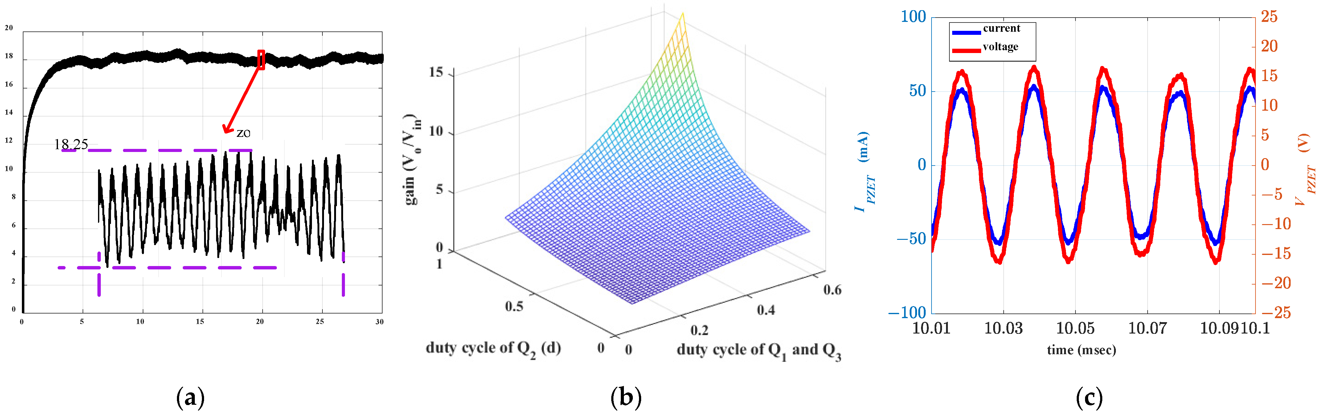
The demonstration of soft switching enabled the checking of the converter gain. According to (14), the converter gain at D = 0.5 and d = 0.75 was about 8. Figure 9a demonstrates that the converter amplified 2.4 V input to 17.9 V in its steady-state operation which proved a gain of 7.45. Therefore, the calculated gain ratio for the converter is approximately correct, and the slight difference between the simulation and calculation analysis values came from the considered estimations during the analytical investigation. According to Figure 9a, the converter has a fast response time, which results from the availability of small size elements in the topology of the converter. The fast response enables the system controller to change output based on the user command as rapidly as possible. The proposed converter gain depends on both switching duty cycles (D and d). Figure 9b demonstrates the converter gain variations vs. sensitive parameters. According to Figure 9b, the increase in D leads to a higher gain, while d increments reduce the converter gain in a constant D.
An H-bridge converter, which was controlled by a 40 kHz sinusoidal pulse width modulation (SPWM) command, was placed at the output of the proposed DC-DC converter to supply the understudy PZET through an LC filter. A regular sinusoidal voltage and currents of the PZET are shown in Figure 9c to prove the acceptable performance of the converter while it was connected to a DC-AC converter.
4. Experimental Results
Due to the lack of a high-voltage and high-power battery package in the available laboratory, the test setup was provided with a smaller rating power. According to earlier explanations, PZETs require about 50–1000 volts in different sea depths (greater sea depth requires higher voltage level). To realistically produce the power density of the industrial version of the studied converter, the element sizes were selected for such a voltage level. Lack of suitable experimental equipment limited us to testing the converter in industrial conditions. As such, a prototype of the proposed converter supplied by a 3.7 V 12.5 Ah Lithium-ion battery package was provided to experimentally validate the soft switching and the converter performance. The battery package included six parallel connected battery cells with 3.7 V and 2 Ah characteristics.
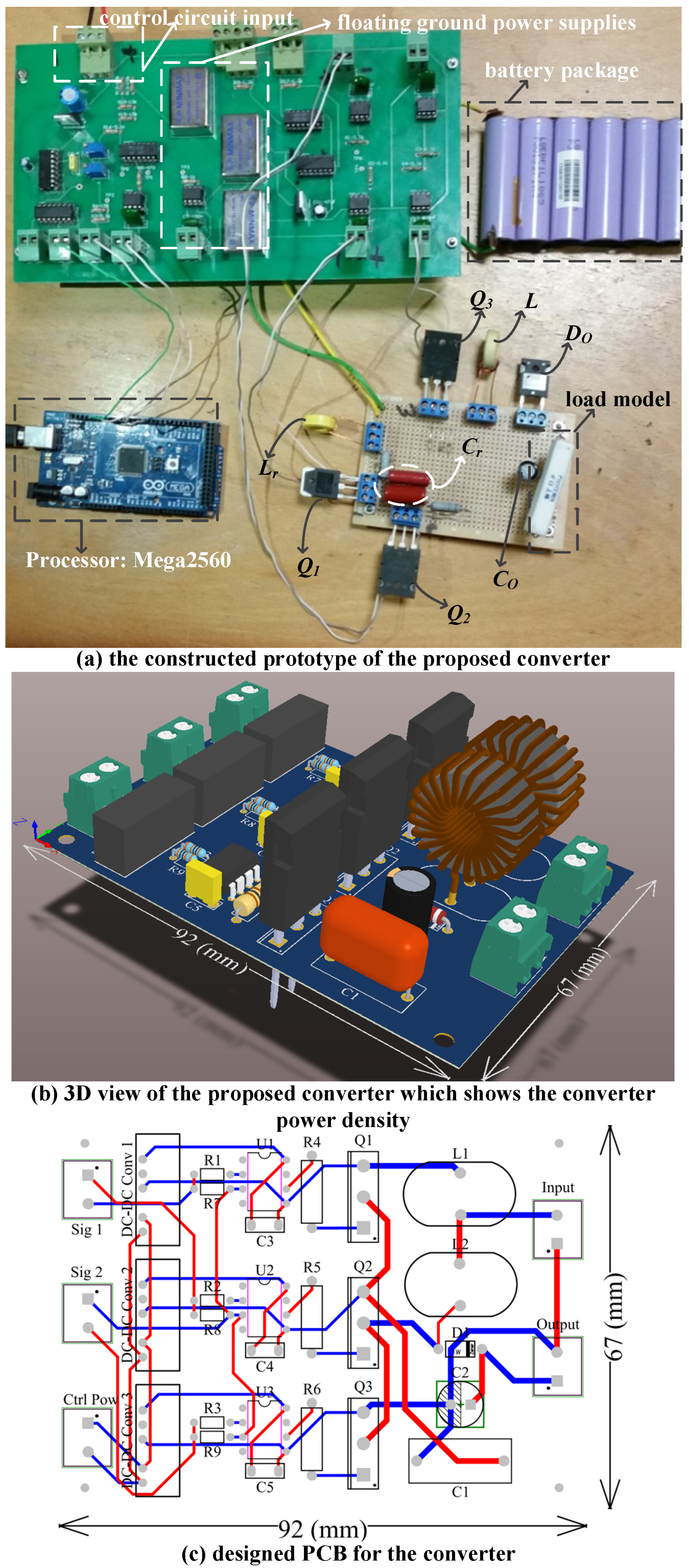
Arduino Mega2560 worked as a microprocessor to generate the required gate pulses presented in Figure 10a. The control pulses of Q1 and Q3 were generated using the first timer of the Mega2560. The required control pulse of Q2 was generated by the second timer of this microprocessor. Although the metal–oxide–semiconductor field-effect transistors (MOSFETs) were the appropriate choice for 100 kHz switching frequency, an insulated-gate bipolar transistor (IGBT) was chosen to examine the converter behavior due to the ability of IGBTs to tolerate higher voltages. Because of the availability of three floating emitter IGBTs in the proposed topology, the gate pulses must command the gate switches through three different isolated ground MinMax power supply (MAU324). Thus, the MinMax power supply used at the output of three separated HCPL 3120 optocouplers provided 15 V voltage to supply the gates. The main structure of the converter included two SGH80N60UFD IGBTs, a FGA25N120ANTD IGBT, and a UF4007 ultrafast diode. Additionally, an electrolyte capacitor with a capacity of 2.2 μF was used to provide the DC-link. The inductors are constructed from the iron powder cores with a permeability of 7.5 μH/m and copper winding.
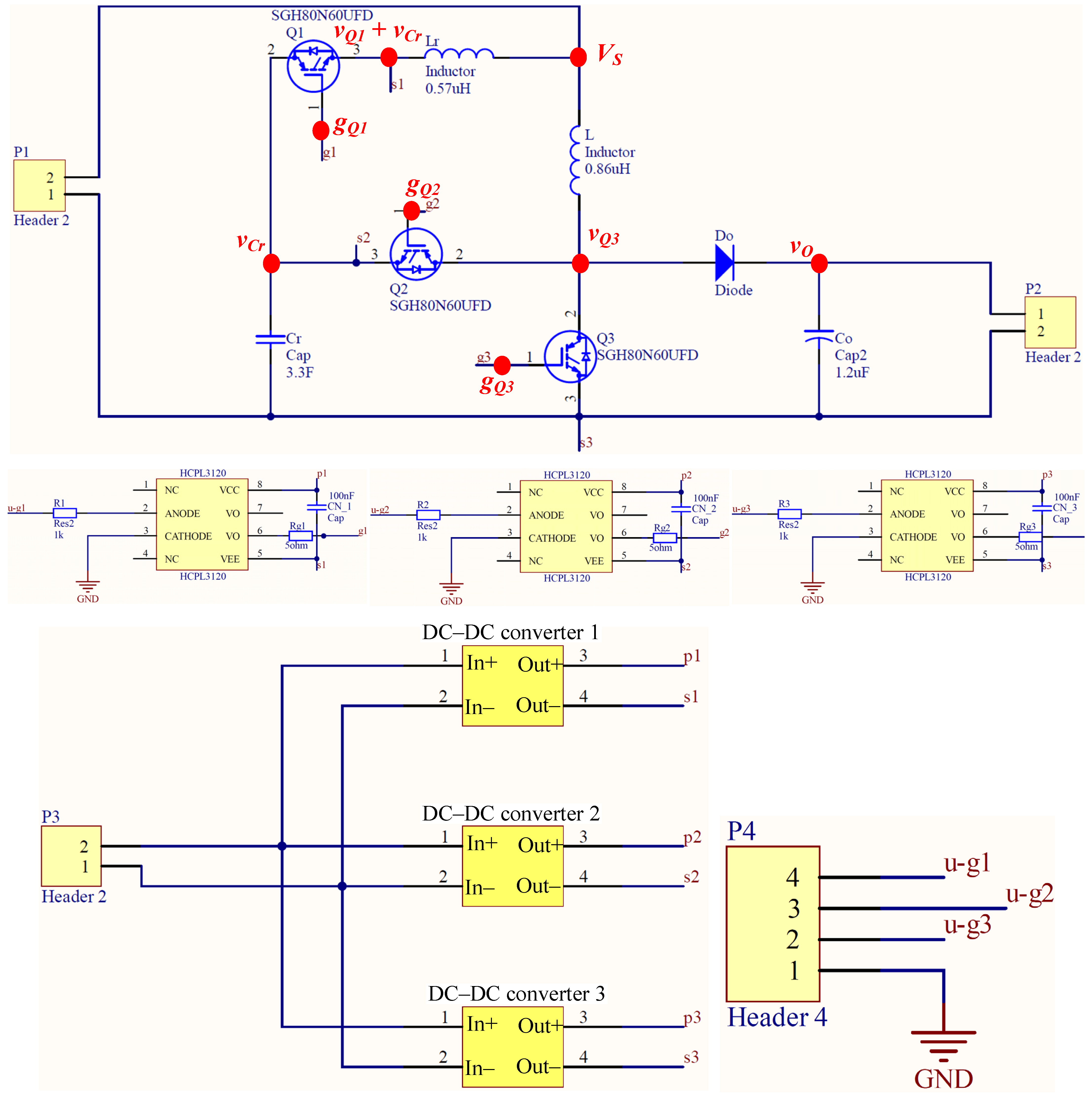
The images in Figure 10b,c show the 3D and printed circuit board (PCB) views of the converter. According to the presented 3D view, the power density of the converter based on the selected switches was about 13 W/cm3 which enabled the converter to be classified as a high-power density converter. The PCB was designed in 2 layers, as shown in Figure 10c. A higher power density is achieved if the PCB is designed in more layers using surface-mount device (SMD) components. The schematic of this design is presented in Figure 11 to show the track paths of the considered PCB. In this figure, P1 and P2 are the input and output terminals of the circuit. The power required to supply the isolated power supplies was provided by P3. P4 was the terminal chosen to provide the gate commands from the controller circuit. R1, R2, and R3 were the input resistors of the opto-coupler. The 5 Ω gate resistance was selected at the output of the opto-couplers to drive the switches.
Measurement of signals in switching power converters is a difficult task. The availability of a two-channel oscilloscope limited us to using the differential measurement technique of signal measurement. In this paper, the gate drive signals were produced using a microcontroller in open-loop condition. It allowed measurement of the produced signal gates when the load was disconnected from the circuit. The currents of the switches were measured by the instalment of 0.3 Ω resistance in the collector emitter path. The grounds of both probes of the oscilloscope were connected to the collector. The voltage of the resistance and voltage of the collector-emitter were measured when the other sides of the probes were connected to the other sides of the series resistor (i.e., installed for current measurement) and emitter. Thus, the voltage and current of the switches were obtained together.
The converter gain is the first factor of the proposed converter that must be examined practically. On the other hand, the proposed converter’s operating duty cycles are limited to . Hence, the experimental verification was performed at the converter operation boundary when the primary duty cycle (D) of the power converter at 100 kHz switching frequency was equal to 20%, as shown in Figure 12a. This figure shows the duty cycle of Q2, which should be 0.25 larger at 45%. The ratio of the converter output to input voltages presented in Figure 12b was about 3.1 which verified the calculated converter gain ratio in (14). The input voltage of the converter shown in Figure 12b, which was provided by the battery package, demonstrated that a large amount of energy was obtained from the battery when the converter switches were turned-on. Therefore, it is evident that the battery voltage drops dramatically in a switching period. However, this energy is sent back to the battery in that period and its voltage is equal to its initial value before the start of the operation period.
The resulting peak in the output voltage waveform, presented in Figure 12b, shows that the main inductor energy was delivered to the load and Co at the end of each switching period. Since the proposed DC-DC converter works an interface circuit between the battery package and an inverter that supplies the PZETs, the charging spikes at the end of each period shown in the waveform of output voltage cannot damage the PZET. These spikes are eliminated by passing through an AC filter. Figure 12c shows Do voltage variation in a switching period, in which the anode voltage is lower than the cathode in the rest of a switching period. Considering both output voltage and diode voltage together, the output is supplied by the converter when the main inductor (L) stored energy is delivered to the load. As shown in Figure 12d, Q1 is turned on in the ZVS condition and the turned-off command meets its gate when its current is zero and enables it to be turned off when the transistor voltage is negative. Furthermore, the ZCS turn-on and ZVS turn-off of the Q2 are presented in Figure 12e. The soft switching turn-on/off of the third switch (Q3) is shown in Figure 12f. Figure 13 shows the simulation results in the same duty cycle and frequency as the experimental results. The small difference between the waveforms resulted from the gate drive circuit of the switches and the parasitic inductances of the wires in the prototyped circuit. The simulation results show the Q1 and Q3 conduct currents together in the same time interval. Q3 starts conduction when Q1 turns off. According to the results, all the switches operate in soft-switching condition. The soft-switching operation reduces the converter switching losses, which inherently increases the converter efficiency.
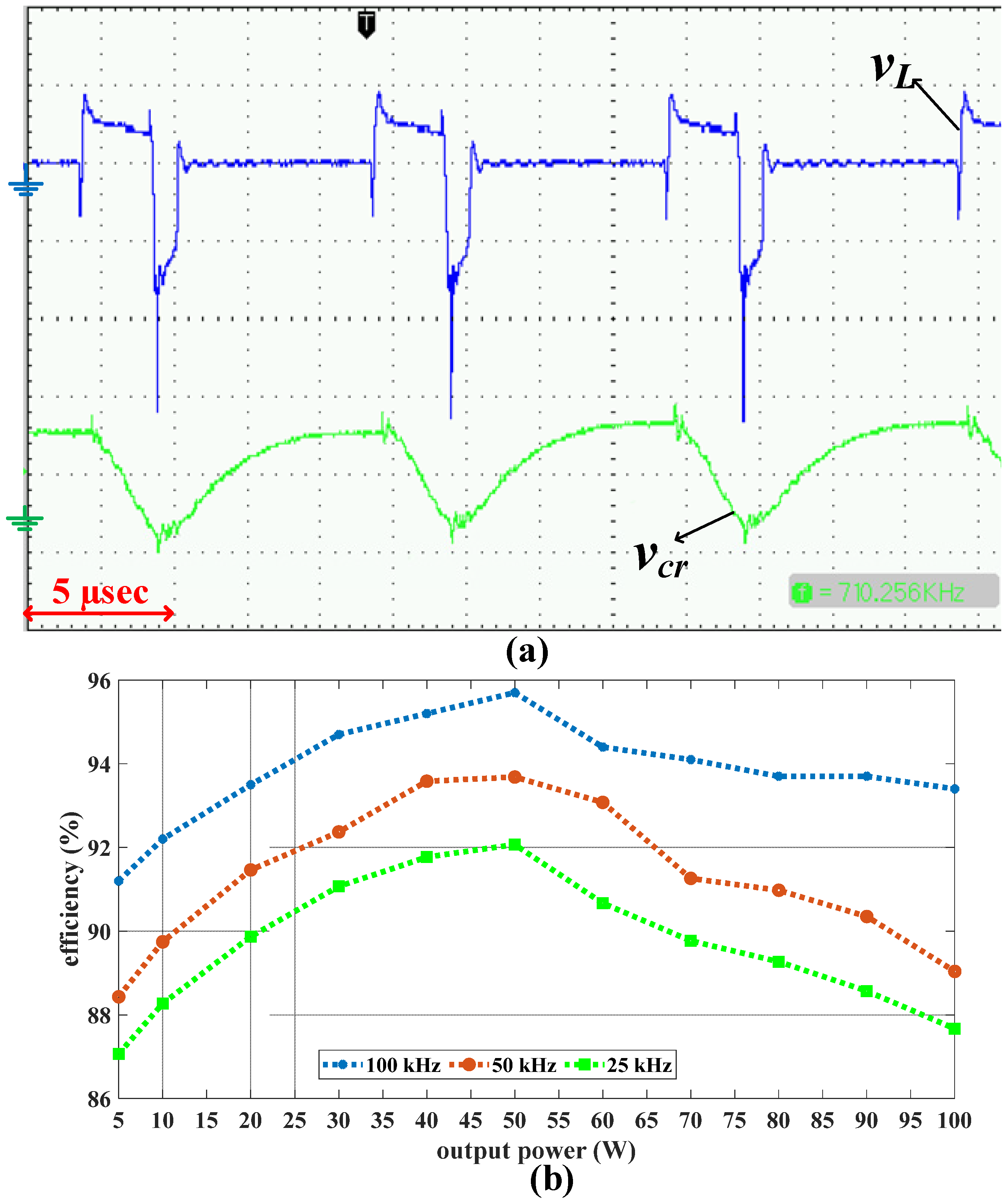
Figure 14a shows the energy conversion between the resonant capacitor and the main inductor. Cr voltage meets its negative peak when it is charged by the battery package through L. Cr voltage starts to increase from the negative peak when both Q1 and Q2 receive the turned-off command and L energy is delivered to Cr through Q2. It should be highlighted that the voltage spike of the inductor occurs when the output diode (DO) starts conduction. The inductor and its resistances are small. The current of the inductor cannot change its direction instantly when the output voltage is connected to one side of the inductor. The small resistance of the inductor cannot provide a large time constant for damping the spike. For this reason, this spike is shown in the provided test setup. This issue is solved if the inductor is provided with a larger resistance.
Note that three 0.3 Ω resistors are placed in series with Q1, Q2, and Q3 emitters to measure the switch currents during operation. For this reason, the voltage/division of the measured signal shown in Figure 12 must be mapped to Ampere/division by consideration of the value of the series resistors.
The proposed converter provides ZVS and ZCS switching for all switches in smaller switching frequencies up to 25 kHz. The resonances occur faster than the smaller switching frequency. Therefore, the energy conversion among the resonance elements occurs several times in a period of switching, which leads to a higher gain in comparison to the chosen based frequency (100 kHz) during the design procedure. In this condition, higher current cross through the switches and windings cause increments of conduction losses. In brief, although working in a lower switching frequency brings about a higher gain in a soft-switching operation, the converter efficiency is decreased because of the increase in conduction losses. To consider the conduction and switching losses in the efficiency analysis of the converter, the converter efficiency curve is extracted experimentally. The efficiency is defined by the ratio of the output active power over input active power. The input and output powers are calculated by multiplication of the input/output voltage and current measured by the digital amperemeters and voltmeters. Figure 14b shows the variation in the efficiency vs. output power in three different switching frequencies.
A similar procedure investigated the uncertainty of the measurement in reporting the results of an analysis on the repeatability, reproducibility, and stability of the measured results, as reported in [36,37]. The temperature variation was considered as an uncertain variable during the test.
According to the repeatability definition, the power converter was tested (turn/on and turn/off) under 100 W operation when the switch temperature was constant in each iteration. The input power was measured using the same means in each test. The collected data after 10 tests demonstrated the repeatability of the results with standard deviation of 0.0179 W. The reproducibility was studied by collecting another set of data on a 100 W experiment at the same switch temperature. The standard deviation of the second set of data was 0.0166 W. Thus, the measured data were reproducible because the difference of the calculated standard deviation was 0.0001 W. Finally, the converter was examined under 100 W loads on four consecutive days. The standard deviation of the collected data over four days was 0.0128 W, which showed the stability of the converter behavior.
5. Conclusions
A high-step-up, high-efficiency, high-power density converter was proposed for driving PZETs. The availability of small-size power components in the structure of the proposed topology helped to decrease the required space of the converter. Because of the soft-switching operation of the converter switches, the converter has a higher efficiency in comparison to the most of the previously proposed high-step-up converters, which work in hard-switching conditions. Such a low-loss converter is suitable not only for driving PZETs but also for use in all other applications where a battery package is used as a power source.
Furthermore, the fast resonance increases the voltage build-up time at the output of the converter during transient conditions. The fast response of the converter is required when the energization time of a load is limited by the users. For instance, in PZETs, users need to energize the piezoelectric in a short time and stop energization to receive data.
Compared to the digital processors, controller designers prefer to use analog circuits in harsh noisy environments. The common input/output ground of the non-isolated converters eases the preparation of the feedback signals, which are required in a closed-loop control circuit. Therefore, the proposed converter is suitable to be utilized in the harsh conditions because of its non-isolated topology. The closed-loop controller design of the system and converter testing with higher power rating will be the subject of study in future works.
Author Contributions
Conceptualization, E.R.; methodology, E.R.; validation, E.R. and H.D.-E.; formal analysis, E.R. and H.D.-E.; investigation, E.R.; resources, S.K. and A.M.; data curation, E.R. and H.D.-E.; writing—original draft preparation, E.R.; writing—review and editing, A.M. and S.K.; visualization, E.R., H.D.-E. and A.M.; supervision, A.M.; project administration, E.R. and A.M. All authors have read and agreed to the published version of the manuscript.
Funding
This research received no external funding.
Institutional Review Board Statement
Not applicable.
Informed Consent Statement
Not applicable.
Data Availability Statement
Not applicable.
Conflicts of Interest
The authors declare no conflict of interest. The funders had no role in the design of the study; in the collection, analyses, or interpretation of data; in the writing of the manuscript, or in the decision to publish the results.
References
- Yang, C.; Wang, T.; Li, Y.; Yang, H.; Li, J.; Qu, D.; Xu, B.; Yang, Y.; Daemen, J. Feasibility analysis of using abandoned salt caverns for large-scale underground energy storage in China. Appl. Energy 2015, 137, 467–481. [Google Scholar] [CrossRef]
- Alanne, K.; Cao, S. An overview of the concept and technology of ubiquitous energy. Appl. Energy 2019, 238, 284–302. [Google Scholar] [CrossRef]
- Deng, Z.D.; Lu, J.; Li, H.; Tian, C.; Myjak, M.J.; Bellgraph, B.J.; Cartmell, S.; Xiao, J. Signal Transmitter and Methods for Transmitting Signals from Animals; Pacific Northwest National Lab. (PNNL): Richland, WA, USA, 2019. [Google Scholar]
- Zhang, W.; Han, G.; Wang, X.; Guizani, M.; Fan, K.; Shu, L. A node location algorithm based on node movement prediction in underwater acoustic sensor networks. IEEE Trans. Veh. Technol. 2020, 69, 3166–3178. [Google Scholar] [CrossRef]
- Kiran, M.R.; Farrok, O.; Abdullah-Al-Mamun, M.; Islam, M.R.; Xu, W. Progress in piezoelectric material based oceanic wave energy conversion technology. IEEE Access 2020, 8, 146428–146449. [Google Scholar] [CrossRef]
- Roshandel, E.; Namazi, M.M.; Saghaian-Nejad, S.M.; Ahn, J.-W. A Step-Up High-Power-Density DC/AC Converter to Drive Piezoelectric Transmitters. In Proceedings of the 2018 21st International Conference on Electrical Machines and Systems (ICEMS), Jeju, Korea, 7–10 October 2018; pp. 688–692. [Google Scholar] [CrossRef]
- Song, H.; Zhang, Y.; Gao, J.; Zhang, Y. Small power ZVS circuits for the marine-controlled source electromagnetic transmitter. J. Eng. 2019, 2019, 4325–4330. [Google Scholar] [CrossRef]
- Choi, H. Prelinearized class-b power amplifier for piezoelectric transducers and portable ultrasound systems. Sensors 2019, 19, 287. [Google Scholar] [CrossRef] [Green Version]
- Smith, N.B.; Webb, A. Introduction to Medical Imaging: Physics, Engineering and Clinical Applications; Cambridge University Press: Cambridge, UK, 2010. [Google Scholar]
- Benson, B.; Li, Y.; Kastner, R.; Faunce, B.; Domond, K.; Kimball, D.; Schurgers, C. Design of a low-cost, underwater acoustic modem for short-range sensor networks. In Proceedings of the OCEANS’10 IEEE Sydney, Sydney, Australia, 24–27 May 2010; pp. 1–9. [Google Scholar] [CrossRef] [Green Version]
- Bhaskar, M.S.; Ramachandaramurthy, V.K.; Padmanaban, S.; Blaabjerg, F.; Ionel, D.M.; Mitolo, M.; Almakhles, D. Survey of DC-DC non-isolated topologies for unidirectional power flow in fuel cell vehicles. IEEE Access 2020, 8, 178130–178166. [Google Scholar] [CrossRef]
- Lu, Y.; Wu, H.; Sun, K.; Xing, Y. A family of isolated buck-boost converters based on semiactive rectifiers for high-output voltage applications. IEEE Trans. Power Electron. 2015, 31, 6327–6340. [Google Scholar] [CrossRef]
- Meraj, M.; Bhaskar, M.S.; Reddy, B.P.; Iqbal, A. Non-isolated DC–DC power converter with high gain and inverting capability. IEEE Access 2021, 9, 62084–62092. [Google Scholar] [CrossRef]
- Zhao, X.; Chen, C.-W.; Lai, J.-S.; Yu, O. Circuit design considerations for reducing parasitic effects on GaN-based 1-MHz high-power-density high-step-up/down isolated resonant converters. IEEE J. Emerg. Sel. Top. Power Electron. 2019, 7, 695–705. [Google Scholar] [CrossRef]
- Lee, S.-W.; Do, H.-L. Isolated High Step-Up Dual-Flyback DC–DC Converter with a Resonant Voltage Multiplier. Electr. Power Compon. Syst. 2020, 48, 871–880. [Google Scholar] [CrossRef]
- Liu, C.; Li, X.; Zhi, Y.; Cai, G. New breed of solid-state transformer mainly combing hybrid cascaded multilevel converter with resonant DC-DC converters. Appl. Energy 2018, 210, 724–736. [Google Scholar] [CrossRef]
- Moradzadeh, M.; Babaei, E.; Zamiri, E.; Hamkari, S. A new high step-up DC/DC converter structure by using coupled inductor with reduced switch-voltage stress. Electr. Power Compon. Syst. 2017, 45, 1705–1719. [Google Scholar] [CrossRef]
- Veerachary, M.; Senjyu, T.; Uezato, K. Modeling of closed-loop voltage-mode controlled interleaved dual boost converter. Comput. Electr. Eng. 2003, 29, 67–84. [Google Scholar] [CrossRef]
- Li, F.; Liu, H. A cascaded coupled inductor-reverse high step-up converter integrating three-winding coupled inductor and diode–capacitor technique. IEEE Trans. Ind. Inform. 2016, 13, 1121–1130. [Google Scholar] [CrossRef]
- Babu, A.R.; Raghavendiran, T.A. High voltage gain multiphase interleaved DC-DC converter for DC micro grid application using ıntelligent control. Comput. Electr. Eng. 2019, 74, 451–465. [Google Scholar] [CrossRef]
- Deng, C.; Yong, M.; Rodriguez, L.A.G.; Balda, J.C.; Li, R. Passive integration using FMLF technique for integrated boost resonant converters. IEEE Trans. Ind. Electron. 2019, 67, 3756–3766. [Google Scholar] [CrossRef]
- Yuan, Y.; Zhang, Z.; Mei, X. Boost-integrated LCL resonant converter with high voltage gain. IET Power Electron. 2020, 13, 332–339. [Google Scholar] [CrossRef]
- Zhu, B.; Ren, L.; Wu, X.; Song, K. ZVT high step-up DC/DC converter with a novel passive snubber cell. IET Power Electron. 2017, 10, 599–605. [Google Scholar] [CrossRef]
- Lin, B.R.; Huang, C.L. Zero voltage switching active clamp buck-boost stage Cuk converter. IET Electr. Power Appl. 2007, 1, 173–182. [Google Scholar] [CrossRef] [Green Version]
- Sayed, K.F.; Nakaoka, M.; Morimoto, K.; Kwon, S.K. New high-frequency linked half-bridge softswitching PWM DC-DC converter with input DC rail side active edge resonant snubbers. IET Power Electron. 2010, 3, 774–783. [Google Scholar] [CrossRef]
- Li, Z.; Wu, T.; Zhang, G.; Yang, R. Hybrid modulation method combining variable frequency and double phase-shift for a 10 kW LLC resonant converter. IET Power Electron. 2018, 11, 2161–2169. [Google Scholar] [CrossRef]
- Roshandel, E.; He, J. High Efficiency High Step-Up DC-DC Converter to Drive Piezo-Electric Transmitters. In Proceedings of the 2019 IEEE Industry Applications Society Annual Meeting, Baltimore, MD, USA, 29 September–3 October 2019; pp. 1–16. [Google Scholar] [CrossRef]
- Mean-Well SD-100C-24, M. 100W Single Output DC-DC Converter. Available online: https://au.mouser.com/ProductDetail/MEAN-WELL/SD-100C-24?qs=sGAEpiMZZMtz8P%2FeuiupSWlCmLAwku1ozA57skhLwW4%3D (accessed on 7 July 2022).
- Yu, D.; Yang, J.; Xu, R.; Xia, Z.; Iu, H.H.-C.; Fernando, T. A family of module-integrated high step-up converters with dual coupled inductors. IEEE Access 2018, 6, 16256–16266. [Google Scholar] [CrossRef]
- Tang, Y.; Tong, H.; Afzal, R.; Guo, Y. High step-up ZVT converter based on active switched coupled inductors. IEEE Access 2020, 1. [Google Scholar] [CrossRef]
- Zhu, B.; Chen, S.; Zhang, Y.; Huang, Y. An interleaved zero-voltage zero-current switching high step-up DC-DC converter. IEEE Access 2020, 9, 5563–5572. [Google Scholar] [CrossRef]
- Hassan, W.; Lu, D.D.-C.; Xiao, W. Single-switch high step-up DC–DC converter with low and steady switch voltage stress. IEEE Trans. Ind. Electron. 2019, 66, 9326–9338. [Google Scholar] [CrossRef]
- Chen, Y.-T.; Lu, Z.-X.; Liang, R.-H. Analysis and design of a novel high-step-up DC/DC converter with coupled inductors. IEEE Trans. Power Electron. 2017, 33, 425–436. [Google Scholar] [CrossRef]
- Rajabi, A.; Rajaei, A.; Tehrani, V.M.; Dehghanian, P.; Guerrero, J.M.; Khan, B. A Non-Isolated High Step-Up DC-DC Converter Using Voltage Lift Technique: Analysis, Design, and Implementation. IEEE Access 2022, 10, 6338–6347. [Google Scholar] [CrossRef]
- Zhu, X.; Zhang, B.; Jin, K. Hybrid nonisolated active quasi-switched DC-DC converter for high step-up voltage conversion applications. IEEE Access 2020, 8, 222584–222598. [Google Scholar] [CrossRef]
- Carobbi, C.F.M.; Lalléchère, S.; Arnaut, L.R. Review of uncertainty quantification of measurement and computational modeling in EMC part I: Measurement uncertainty. IEEE Trans. Electromagn. Compat. 2019, 61, 1690–1698. [Google Scholar] [CrossRef]
- Cepova, L.; Kovacikova, A.; Cep, R.; Klaput, P.; Mizera, O. Measurement system analyses-gauge repeatability and reproducibility methods. Meas. Sci. Rev. 2018, 18, 20. [Google Scholar] [CrossRef] [Green Version]
Figure 1.
Graphical abstract of the operation of PZETs in underwater transmission systems.

Figure 2.
The proposed DC-DC power converter topology with highlighted resonant elements.

Figure 3.
Circuit configurations of the proposed converter in different operation modes. The dashed line shows the current paths in each time interval. The green, blue, and purple are used to distinguish the Q1, Q2, and Q3 from each other. Any gray switch shows that the switch is off in the mentioned time interval.

Figure 4.
Selected waveforms of the converters in a switching period. The solid lines are used to represent the current waveforms of each component. The voltage waveforms are presented by the dashed lines. The gate pulses are shown by dotted lines. In this figure, gQ1, gQ2, and gQ3 show the gate pulses of Q1, Q2, and Q3, respectively. The voltage and current of each switch are shown by vQx, and iQx where x is the switch number defined in Figure 2. The main inductor current, diode current (Do), and resonant capacitor current are shown by iL, iD, and iCr, respectively.

Figure 5.
Estimation of IL based on the average value of the input current.

Figure 6.
Gate pulses of the switches at the simulated test point.

Figure 7.
Soft-switching operation of the converter switches in simulation.

Figure 8.
Simulated current waveforms of the resonance elements and output energizing current of the proposed converter.
Figure 8.
Simulated current waveforms of the resonance elements and output energizing current of the proposed converter.

Figure 9.
(a) Voltage response of the studied step-up DC-DC converter, which shows fast transients, high gain, and low ripple of the DC-link voltage in a simulation study. (b) Gain variations of the proposed DC-DC power converter against simultaneous changes of the switches’ duty cycles in a simulation study. (c) PZET current and voltage waveforms in the simulation.

Figure 10.
The constructed prototype and considered industrial version.

Figure 11.
Schematic of the proposed converter.

Figure 12.
Experimental validation of the proposed converter gain and soft switching. The time division of all presented images in this figure is 2.5 μs. (a) Control signals (2 V/div); (b) output voltage (5 V/div), input voltage (2 V/div); (c) diode voltage (5 V/div); (d) Q1 voltage (5 V/div), Q1 current (1.66 A/div); (e) Q2 voltage (2 V/div), Q2 current (0.66 A/div); (f) Q3 voltage (2 V/div), Q3 current (0.66 A/div).

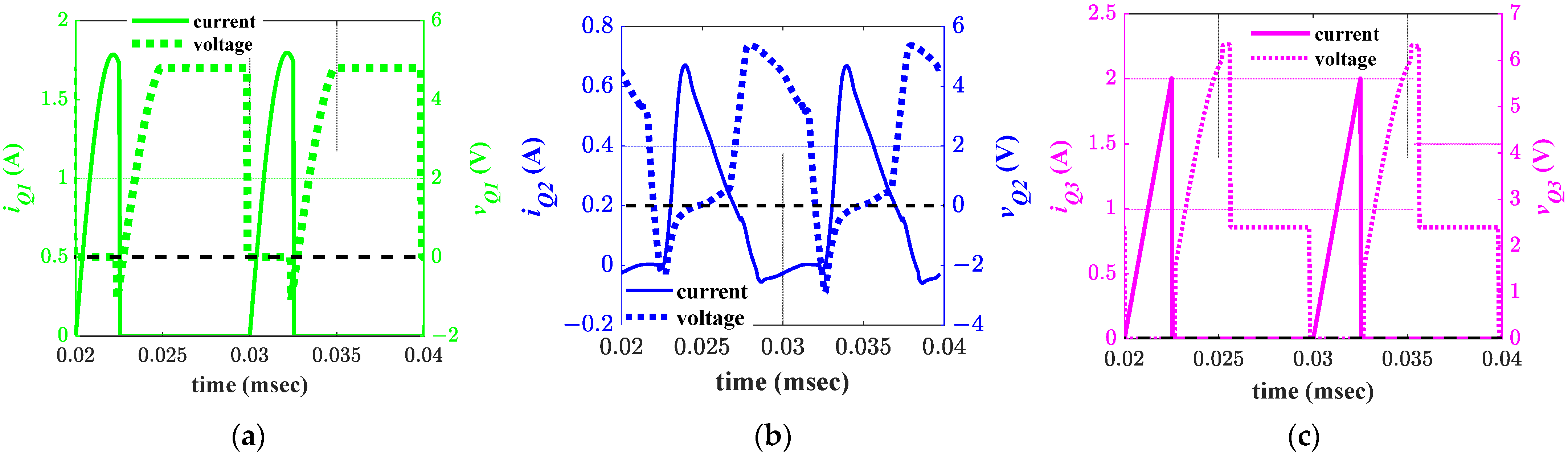
Figure 13.
The simulation results showing the soft switching of the switches in the test conditions (D = 0.2 and d = 0.45). (a) Q1 voltage and current; (b) Q2 voltage and current; (c) Q3 voltage and current.
Figure 13.
The simulation results showing the soft switching of the switches in the test conditions (D = 0.2 and d = 0.45). (a) Q1 voltage and current; (b) Q2 voltage and current; (c) Q3 voltage and current.

Figure 14.
(a) Cr voltage (5 V/div) and L voltages (2 V/div) with time division of 2.5 μs. (b) Experimentally measured efficiency vs. output power of the prototyped DC-DC converter at different switching frequencies.
Figure 14.
(a) Cr voltage (5 V/div) and L voltages (2 V/div) with time division of 2.5 μs. (b) Experimentally measured efficiency vs. output power of the prototyped DC-DC converter at different switching frequencies.


Table 1.
Comparison of the proposed DC-DC power converter element size vs. two other high-step-up converters in the literature.
Table 1.
Comparison of the proposed DC-DC power converter element size vs. two other high-step-up converters in the literature.
| The Proposed Converter | Ref [32] | Ref [33] | Ref [34] | Ref [35] | |
|---|---|---|---|---|---|
| Converter power | 120 W | 120 W | 200 W | 200 W | 200 W |
| Switching frequency | 25–100 kHz | 100 kHz | 60 kHz | 50 kHz | 30 kHz |
| Maximum Efficiency | 95.8% | 96.7% | 94.5% | 93.1% | 92.5% |
| Operating duty cycle | 0.2–0.75 | 0.3–0.7 | 0.5–0.9 | 0.1–0.75 | 0.05–0.3 |
| Number of inductors | 2 | 1 | 4 | 2 | 2 |
| Inductors’ value | L = 0.86 μH, Lr = 0.57 μH | Lm= 50 μH, Lk = 1.1 μH | L1 = L2 = 1.4 μH, L3 = L4 = 100 μH | Lm = 100 μH, Lk = 300 μH | L1= L2= 220 μH |
| Number of capacitors | 2 | 5 | 4 | 3 | 4 |
| Capacitors’ value | Cr = 3.3 μF, Co = 1.2 μF | C1 to C4 = 30 μF, Co = 47 μF | C1 = C2 = 5 μF, C3 = C4 = 220 μF | C1 = 470 μF, C2 = 1000 μF, C3 =100 μF | C1 = C2 = C3 = 100 μF, C4 = 220 μF |
| Number of diodes | 1 | 5 | 4 | 3 | 4 |
| Number of switches | 3 | 1 | 2 | 2 | 2 |
Publisher’s Note: MDPI stays neutral with regard to jurisdictional claims in published maps and institutional affiliations. |
© 2022 by the authors. Licensee MDPI, Basel, Switzerland. This article is an open access article distributed under the terms and conditions of the Creative Commons Attribution (CC BY) license (https://creativecommons.org/licenses/by/4.0/).
Share and Cite
MDPI and ACS Style
Roshandel, E.; Mahmoudi, A.; Kahourzade, S.; Davazdah-Emami, H. DC-DC High-Step-Up Quasi-Resonant Converter to Drive Acoustic Transmitters. Energies 2022, 15, 5745. https://doi.org/10.3390/en15155745
AMA Style
Roshandel E, Mahmoudi A, Kahourzade S, Davazdah-Emami H. DC-DC High-Step-Up Quasi-Resonant Converter to Drive Acoustic Transmitters. Energies. 2022; 15(15):5745. https://doi.org/10.3390/en15155745
Chicago/Turabian StyleRoshandel, Emad, Amin Mahmoudi, Solmaz Kahourzade, and Hamid Davazdah-Emami. 2022. "DC-DC High-Step-Up Quasi-Resonant Converter to Drive Acoustic Transmitters" Energies 15, no. 15: 5745. https://doi.org/10.3390/en15155745
Note that from the first issue of 2016, this journal uses article numbers instead of page numbers. See further details here.