
Rapid Evaluation Method for Modular Converter Topologies


Supergrid Institute, 69100 Villeurbanne, France
*
Authors to whom correspondence should be addressed.
Energies 2022, 15(10), 3492; https://doi.org/10.3390/en15103492
Submission received: 30 March 2022
/
Revised: 6 May 2022
/
Accepted: 7 May 2022
/
Published: 10 May 2022
(This article belongs to the Topic Power Converters)
Abstract
:The success of modular multilevel converters (MMCs) in high-voltage direct current (HVDC) applications has fueled the research on modular converter topologies. New modular converter topologies are often proposed, discussed, and sometimes applied in HVDC, as well as other industrial application such as STATCOMs, DC/DC HVDC, medium-voltage direct current (MVDC), etc. The performance evaluation of new modular converter topologies is a complex and time-consuming process that typically involves dynamic simulations and the design of a control system for the new converter topology. Sadly, many topologies do not progress to the implementation stage. This paper proposes a set of key performance indicators (KPIs) related to the cost and footprint of the converter and a procedure designed to rapidly evaluate these indicators for new converter topologies. The proposed methodology eliminates the need for dynamic simulations and control-system design, and is capable of identifying whether a particular converter is worth considering or not for further studies of a specific application, depending on the operating requirements. Thanks to the method outlined in this work and via the key parameters quantifying the “relevance” of the analyzed converters, promising topologies were easily identified, while the others could be rapidly discarded, resulting in saving valuable time in the study of the solutions that have a real potential. The proposed method is first described from a general point of view and then applied to a case study of the new converter topology—Open-Delta CLSC—and its application in two use cases.
1. Introduction
High-voltage direct current (HVDC) technology nowadays represents the most advantageous technical solution to problems such as long-distance energy transmission, asynchronous AC system interconnection, interconnection of different regions requiring submarine and underground cables, and transmission of offshore wind power to shore [1,2]. The ability to efficiently connect large renewable energy sources located far away from the main loads is rapidly expanding the installation of HVDC lines in areas such as northern Europe and across China [3,4,5,6].
The crucial elements of HVDC transmission, from both a technological and ultimately a cost point of view, are the power electronic converters, which allow the AC/DC energy conversion and vice versa. Thus, a great amount of research has been and still is currently directed toward the investigation of new and more advantageous HVDC converter topologies. The modular multilevel converter (MMC) [7] currently represents the most accepted solution in new installations, in spite of the many variations that have been proposed [8,9,10,11] and the many more new topologies that have attempted to challenge it [12,13,14,15] (to cite only a few of them).
The advantages of the MMC, such as independent active and reactive power controls, modularity, and reduced filtering requirements, have made this modular technology interesting even in other applications such as STATCOMs [16] and HV DC-DC converters, [17,18] and in medium-voltage (MV) applications [19].
To understand whether a new topology is beneficial and can potentially compete in the marketplace with established designs, one should identify the key strengths of the proposed solution and any potential weaknesses. This process should be done in the most efficient manner possible in order to discard topologies that do not bring significant benefits early in the development process. A typical approach is to define a set of key performance indicators (KPIs), but it is difficult to find a general agreement on what those KPIs should be, as the works comparing different topologies often make use of different ones [17,18]. A significant attempt to harmonize them can be traced to [20]. Moreover, a typical approach to calculation of KPIs adopted up to now involves an extensive use of dynamic simulations, even for the calculation of steady-state parameters and the acquisition of steady-state waveforms. The main drawbacks of this approach can be summarized in the following two points: (1) running simulations makes it necessary to design the control system, which is not a straightforward and quick task, especially for new topologies; and (2) for a complete evaluation of the converter performance, multiple simulations must be run in order to analyze the behavior in different operating conditions, which takes valuable time. Such an approach is especially wasteful when it is found that benefits offered by the new topology are not enough to justify commercial interest compared to an already-established solution in the market.
In this paper, we formalize a methodology that can be applied to the assessment of a new converter topology in much more efficient manner and that does not require a substantial simulation effort to assess whether further development of the converter topology is worth pursuing for a particular application. This methodology rapidly provides the data necessary for a manufacturer to choose whether the converter under scrutiny has no interest or represents a valid solution, thereby justifying additional studies on it. To the best of the authors’ knowledge, there are no papers that describe and discuss similar general procedures. In addition, we identify and propose a set of general KPIs that can be used universally in the assessment of topologies with different weightings applied, depending on the application. A practical application of the proposed methodology is also presented in order to demonstrate the efficiency of the method.
The paper is structured as follows. In Section 2, the methodology is presented, and particular aspects of its application are discussed. In Section 3, generic KPIs are defined and a calculation method is presented. In Section 4 and Section 5, the proposed methodology is applied in a case study of a new topology called the “Open-Delta Capacitor Link Series Converter (CLSC)” [21], which is compared to the half-bridge modular multilevel converter (MMC) used as a reference topology. Finally, in Section 6, the KPIs are presented and compared for the topologies under study. The conclusions drawn in given in Section 7.
2. Topology Assessment Methodology
The goal of the proposed methodology was to minimize the development effort required to identify whether a new topology can be a serious contender to replace an existing design in practical applications. Such a methodology must avoid the necessity of the control-system design and the repetition of a significant number of simulations, so that weak topologies can be immediately identified and discarded, while time can be saved and better invested in analyzing converter architectures that have a real potential. To address this goal, we proposed to focus our analysis on the steady-state operation of the topology; if no significant benefits are shown, it is unlikely the topology would be of interest in industrial applications, and there would be no need to develop it further.
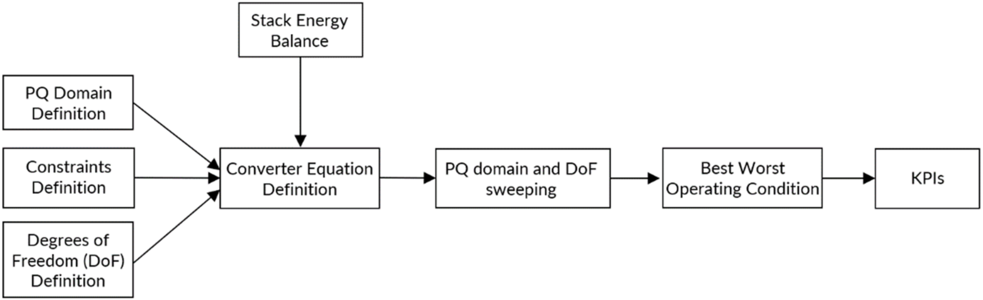
A simplified block diagram of the proposed procedure is shown in Figure 1. It begins with the definition of the requirements of the application and identification of the topology optimization approached, followed by the derivation of the converter equations that shall consider the energy balance within the converter. Theoretical investigation are continued with the implementation of the derived equations in a mathematical analysis tool such as MATLAB. Once implemented, the full operation domain can be swept quickly to identify the best and worst operation conditions and compute the associated KPIs. These steps are explained in detail in the next section.
2.1. Definition of the PQ Operating Domain
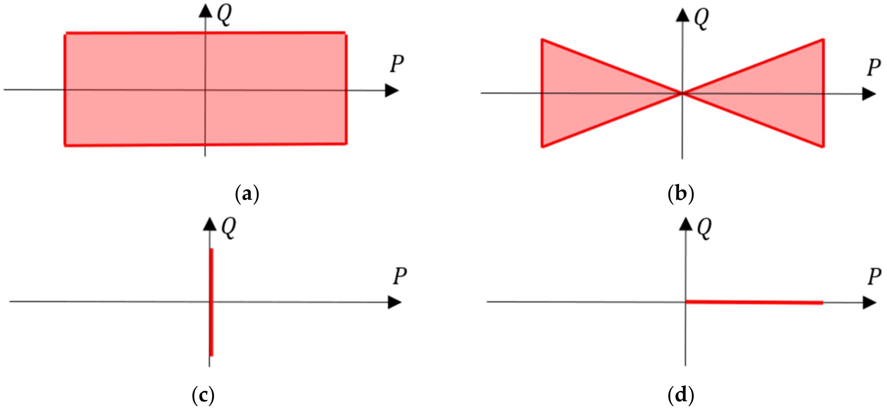
When assessing the benefits of a topology, it is very important to define the application and the requirements that are expected by the converter in the target application. It might be tempting to define the widest requirements possible to cover all possible applications; this approach is interesting academically, but it can miss some of the topologies that can bring advantages to one application but cannot be applied universally. Moreover, this approach can lead to oversizing of the converter. In a grid-connected converter, the key features defining the operating domain are the requirements for the active and reactive power values that the converter must provide. These determine the “PQ-domain” for which the converter must be sized.
Four different PQ-domains can be identified for applications within electrical grids. These profiles are shown in Figure 2. The rectangular PQ domain [22] shown in Figure 2a is common in HVDC applications, and represents the maximum requirements. On the other hand, for converters used in medium-voltage direct current (MVDC) applications, a “butterfly PQ domain” [23] is more common; this domain is characterized by the fixed minimum as shown in Figure 2b. Other typical PQ domains are represented by the STATCOM shown in Figure 2c and the MVDC load converter shown in Figure 2d. In the case of STATCOM, the domain can be asymmetrical; i.e., the max inductive power is greater than the max capacitive power (or vice versa). For MV loads, the converter only absorbs the active power, and the sign of the active power never changes.
2.2. Definition of Constraints and Degrees of Freedom
It is usually possible to optimize/design a topology in different ways that somehow depend on the application. Therefore, it is important to decide which parameters of the topology shall be fixed and which ones can be changed to achieve the optimum design. This leads to the definition of the:
- Degrees of freedom—parameters used to optimize the overall sizing.
- Constraints or constant parameters—parameters that must be the same for all the converter topologies in order to allow for a fair comparison between them.
These parameters change depending on the topology and the application. To provide some guidance, typical options are presented below.
- Typical degrees of freedom:
- Transformer secondary side voltage.
- Typical constant parameters:
- Submodule rated voltage;
- Maximum stack voltage ripple;
- Maximum DC voltage ripple.
2.3. Definition of the Steady-State Characteristic Equations Guaranteeing the Converter Energy Balance
The next step is to write the characteristic equations of the converters in a steady state based on the parameters reflecting constraints and degrees of freedom, as well as the PQ operating domain. This means analytically defining the current and voltage across each element of the topology. At this stage, only the ideal voltage and current waveforms during steady-state operation are considered. This implies that the voltage of the stacks does not present the staircase shape, which is characteristic of multilevel converters, but is rather assumed to be smooth and as close as possible to its ideal waveform. For most applications, the waveforms are considered to have just DC and one AC components.
An important point to consider during this stage is the energy balance inside the converter, and each single stack must be satisfied; i.e., , where is the instantaneous energy stored in the stack and is the fundamental period. Moreover, for sizing purposes, the components are considered to be ideal; i.e., all the power losses are neglected. This means that the waveforms are calculated while assuming that the component voltage drops have a negligible impact on them. The waveforms computed with this assumption are later used to calculate losses.
2.4. PQ Domain Sweeping, Sizing Work Point Identification, and KPI Calculations
Once the characteristic equations have been defined, the entire PQ operating domain can be swept in order to identify the most critical operating condition, on which the converter sizing has to be based. At the same time, the degrees of freedom must be selected so that the most advantageous sizing in the most critical working conditions is obtained.
Finally, all the KPIs are computed and are ready to be compared between the topologies under investigation.
3. Converter KPI Identification
As described in [24], the interest in a particular converter configuration depends mainly on the converter’s cost, size, and efficiency. The cost data is normally confidential, and only manufactures can accurately assess it. Regarding converter size, at least a preliminary design must be established to estimate the converter’s footprint. For that, the size of each element should be roughly assessed, as well as the needed clearance distance between them. This is not generally done during the early stages of development of a new promising topology, as it requires a good understanding of the considered topology. Therefore, it is important to identify the parameters or KPIs able to suitably represent those aspects without entering into a time-consuming detailed design.
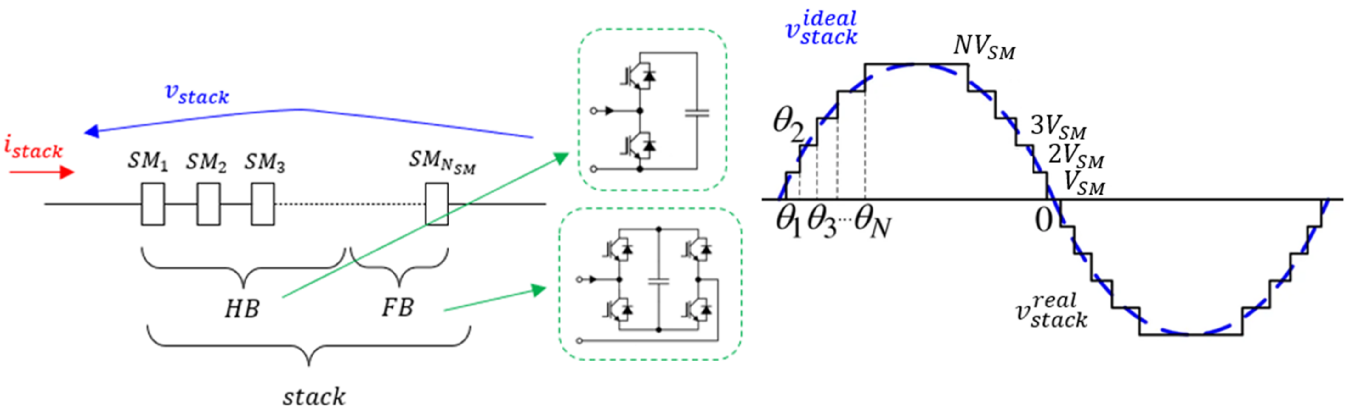
Before presenting the KPIs, it is important to define the basic element of a modular converter, commonly known as the “stack”. The term “stack” is usually adopted to describe a certain number of submodules, which can be both of the half-bridge (HB) and/or the full-bridge (FB) type, which are connected in series as depicted in Figure 3. The voltage created by the stack is given instant-by-instant by the number of capacitors that are inserted in the circuit, and it is characterized by the typical “staircase” profile. Whereas the considered in this study is the first harmonic approximation of the instantaneous voltage . A “stack” is further characterized by , the total number of SMs inside it; and , the rated SM voltage.
This structure is used in MMCs, as well as in STATCOMs, cascaded H-bridges (CHB), and other converters adopted for the AC/DC or DC/DC conversion in HVDC or MVDC applications.
In our view, the KPIs presented below provide a solid basis on which the converter costs and footprint can be evaluated in the early stages of development.
- Transformer number and their sizing power (). these parameters are related to the cost and volume of the transformers. In HVDC applications, single-phase transformers are usually preferred over three-phase transformers (due to transportation constraints) and, as long bushings and clearance distances are needed, the number of transformers has a significant impact on the station footprint. This KPI is highlighted here; even if the standard number of transformers is three for AC/DC HVDC converters, it can be different for other topologies.
- Submodule (SM) number (). In the set of the KPIs proposed, this represents the footprint of the converter to the highest degree. It is related to the number of interconnections between the submodules and mechanical assemblies, the number of capacitor voltages to measure, and the number of discharge circuits (as well as the number of bypass circuits, depending on the manufacturer’s technical choices). As the submodules correspond to the major cost of the converter, they also relate to the cost, but other KPIs provide a better representation of the cost.
- Semiconductor switch total sizing power (). This is related to the “quantity of silicon” (voltage the semiconductors must withstand and the current passing through them), and therefore is related to the converter cost. In simple terms, it represents the sum of the sizing power of all the switches.
- DC voltage ripple (). This is related to the converter’s cost and volume, as it indicates whether an additional filter is needed on the DC side.
- Submodule cell capacitance (). This is mainly related to the SM size (which is important regarding its ability to handle it during the construction phase and during replacement operations for faulty ones). It is also related to the energy stored in an individual submodule, which is a constraint for the devices in the fault current path in the case of an SM internal short-circuit.
- Stored energy (). This parameter quantifies the energy stored in the converter, which is mainly due to the SM capacitors (but it also takes into account the energy stored in the inductors), which represent the major part of the SM volume. Therefore, this parameter is linked to the converter volume.
- Switch number (). This has a main influence on cost.
- Power loss (). This is related to the converter’s efficiency and then the operation costs, but also to the constraints on the thermal-management system (impacts on cost and footprint).
Most of the KPIs defined above are straightforward; however, some others must be clearly defined mathematically. More specifically, a closer focus must be placed on the calculations of the SM capacitance and the total switch sizing power
3.1. Per Unit System
In this paper, the calculations were carried out on a per unit (PU) basis in order to generalize the results and the comparison between topologies. The bases used for the PU calculations were:
- The DC voltage ;
- The maximum DC current ;
- The power base, which is given by: .
3.2. Submodule Capacitance Calculation
The sizing of the submodule capacitors was carried out by following the approach described in [25]. For a given submodule stack, the submodule capacitors can be found using the following equation:
where is the number of submodules in the stack, is the submodule rated voltage on a PU basis, and is the maximum stack voltage variation allowed, defined as:
where is the instantaneous number of SMs inserted in the circuit, is the istanteneus stack voltage in V, and is the rated SM voltage in V, is the maximum energy variation over the period, and it can be found by using the following equation:
where:
In which:
Please note that the unit of is seconds; namely: .
3.3. Total Semiconductor Switch Sizing Power
The total semiconductor switch sizing power for a single stack depends on the maximum current and voltage ratings of the stack and the type and the number of the submodules in the stack, and is defined by Equation (7):
where and are the numbers of HB and FB SMs in the stack, respectively. Knowing that:
and
then:
in which:
In other words, Equation (7) is the sum of the power ratings of each switch of the converters, and therefore is linked to the “quantity of silicon” necessary.
3.4. Power Loss
To calculate power losses, a choice of the semiconductor device must be made. Once this choice has been made, then power losses can be evaluated. To estimate the power loss, both conduction and switching losses must be evaluated. For high-power MMC converters, the device’s switching frequency is close to the line frequency, and switching losses contribute less than 25% of the total losses; these are highly dependent on the capacitor voltage-balancing algorithm (VBA) and cannot be analytically calculated. Moreover, conduction losses and switching losses are related to the number of switches and the current passing through them. Therefore, we proposed to concentrate on the conduction losses only as the indication of the converter’s efficiency.
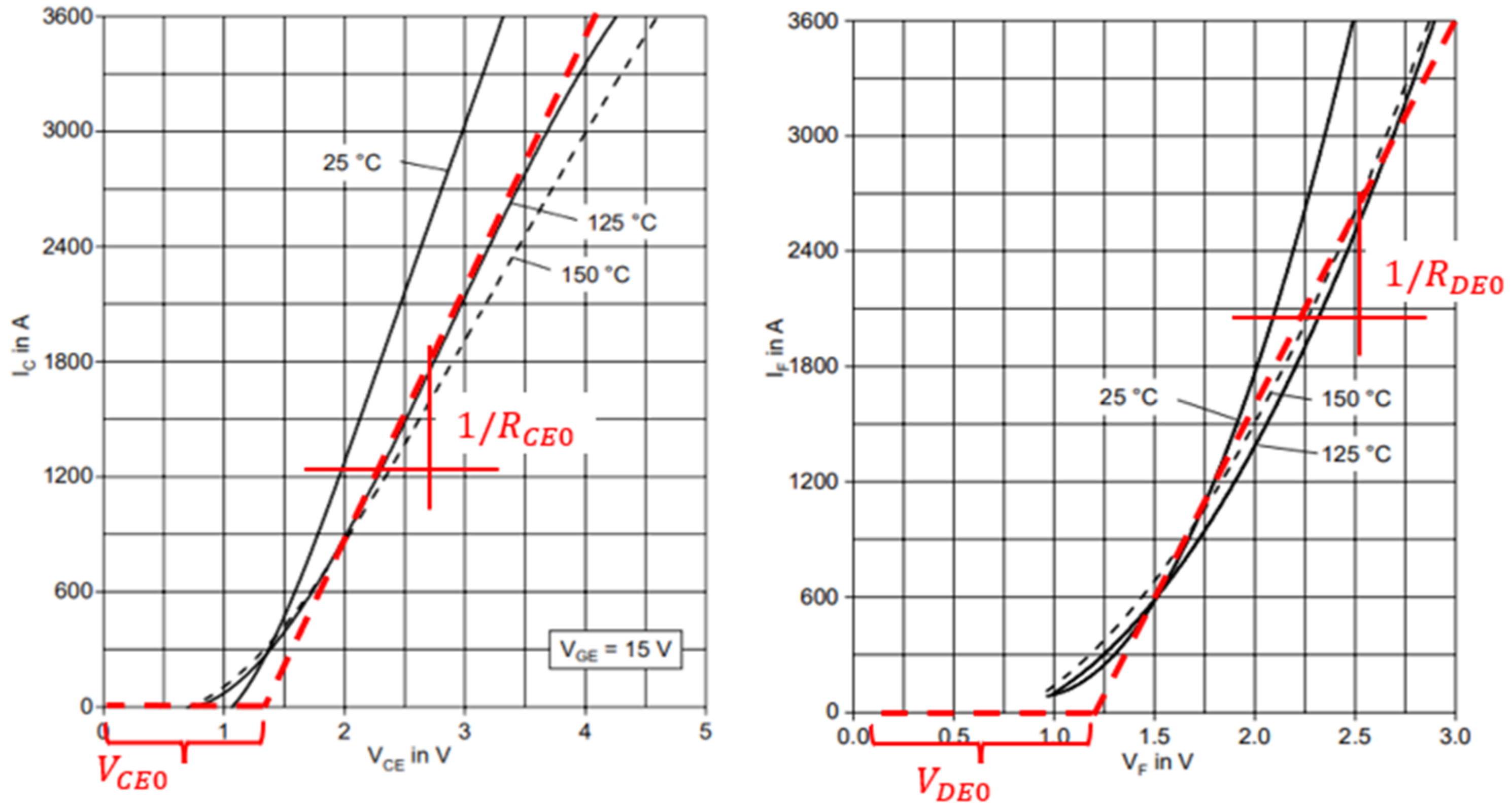
Without a loss of generality, when considering an IGBT, its conduction power losses are quantified by the following relation:
where is the IGBT collector–emitter voltage and is the collector current. It can be easily proven that:
where and can be extracted from the manufacturer’s datasheet, as shown in Figure 4; is the mean value of the absolute value of the collector current; and is the rms collector current. The same procedure can be applied to the free-wheeling diode.
Once the conduction power loss is defined for the single switch, the total conduction power loss calculation can be extended to the entire converter, as shown in the following sections.
4. Definition of Case Studies
To demonstrate the proposed methodology, it was applied to a new topology called the “Open-Delta Capacitor Link Series Converter (CLSC)” [21], which was compared to the half-bridge modular multilevel converter (MMC) that was used as a reference topology. In order to demonstrate the importance of the defining target application when analyzing new topologies, two scenarios were considered. These two scenarios were defined by different PQ domains, as they corresponded to different real applications (HVDC and load converter). In the first scenario, a rectangular PQ domain was used; for the second scenario, a zero-Q load was used.
The characteristic equations are reported as a function of the PQ work point, the degrees of freedom, and the constraints.
For the analysis of the topologies, a PU system based on DC side values was adopted as described in Section 3.1. For both topologies, the secondary transformer voltage (peak value, phase to phase) Rv was considered as a degree of freedom. It was defined as:
4.1. MMC
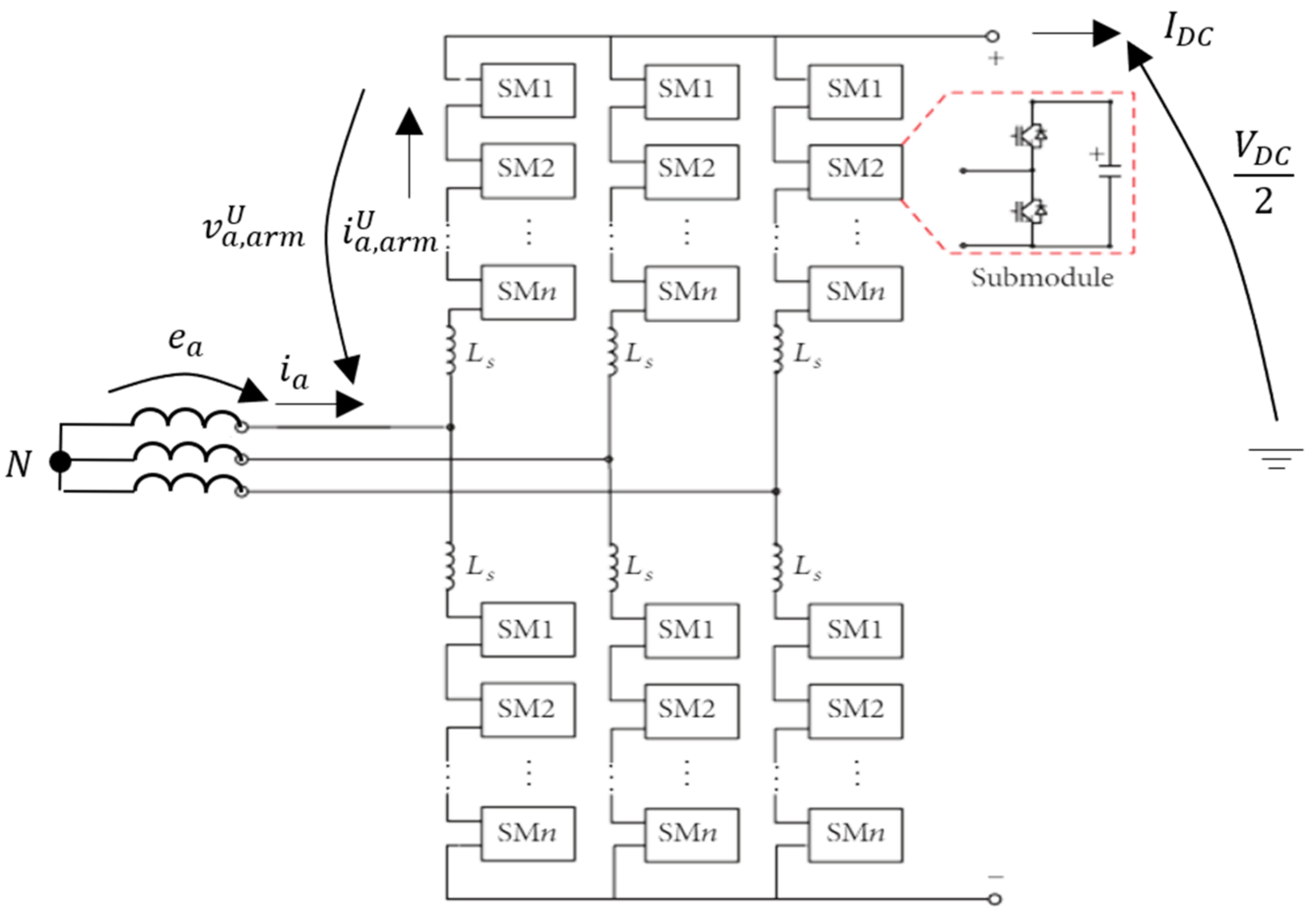
The well-known structure of the MMC is shown in Figure 5.
To derive steady-state equations for the converter, the following assumptions were made:
- The voltage drop determined by the transformer was negligible.
- The voltage drop on the arm inductance was negligible.
- The DC current source was ideal.
With reference to Figure 5, and considering the upper arm connected to the a phase, one has in PU:
where:
The second term in the formula describes a third harmonic injection with the following amplitude [26]:
where .
On the other hand, the AC components of the current are defined as:
where:
in which:
where and are the active and reactive power in PU, respectively:
It could be easily verified for all , and that the arm energy balance was satisfied; in other words, the condition , where (for a 50 Hz system) and is defined as follows:
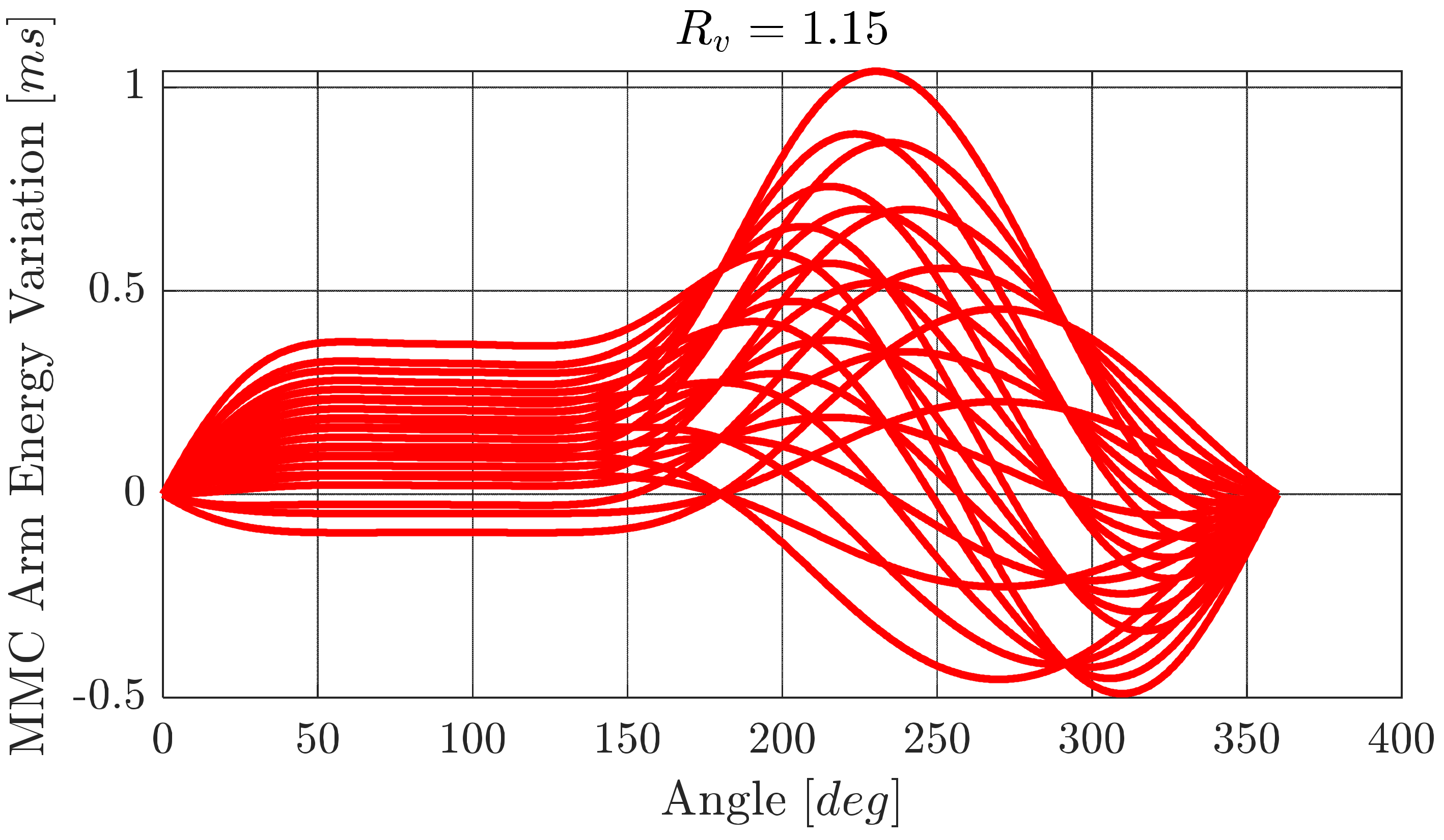
The MMC equations as a function of , and that were able to satisfy the arm energy balance in every operating condition were obtained. These equations were implemented in a MATLAB script able to sweep a large number of working points in the expected PQ domain and return the sizing of the converter based on the most critical condition. Figure 6 shows the energy variation over the period for the following and values: , ; and for .
Considering that at any given time, only half of the switches in the submodule conducted the current, then conduction current losses could be calculated according to (25):
where: and , and represents the number of installed arm switches.
4.2. Open-Delta CLSC
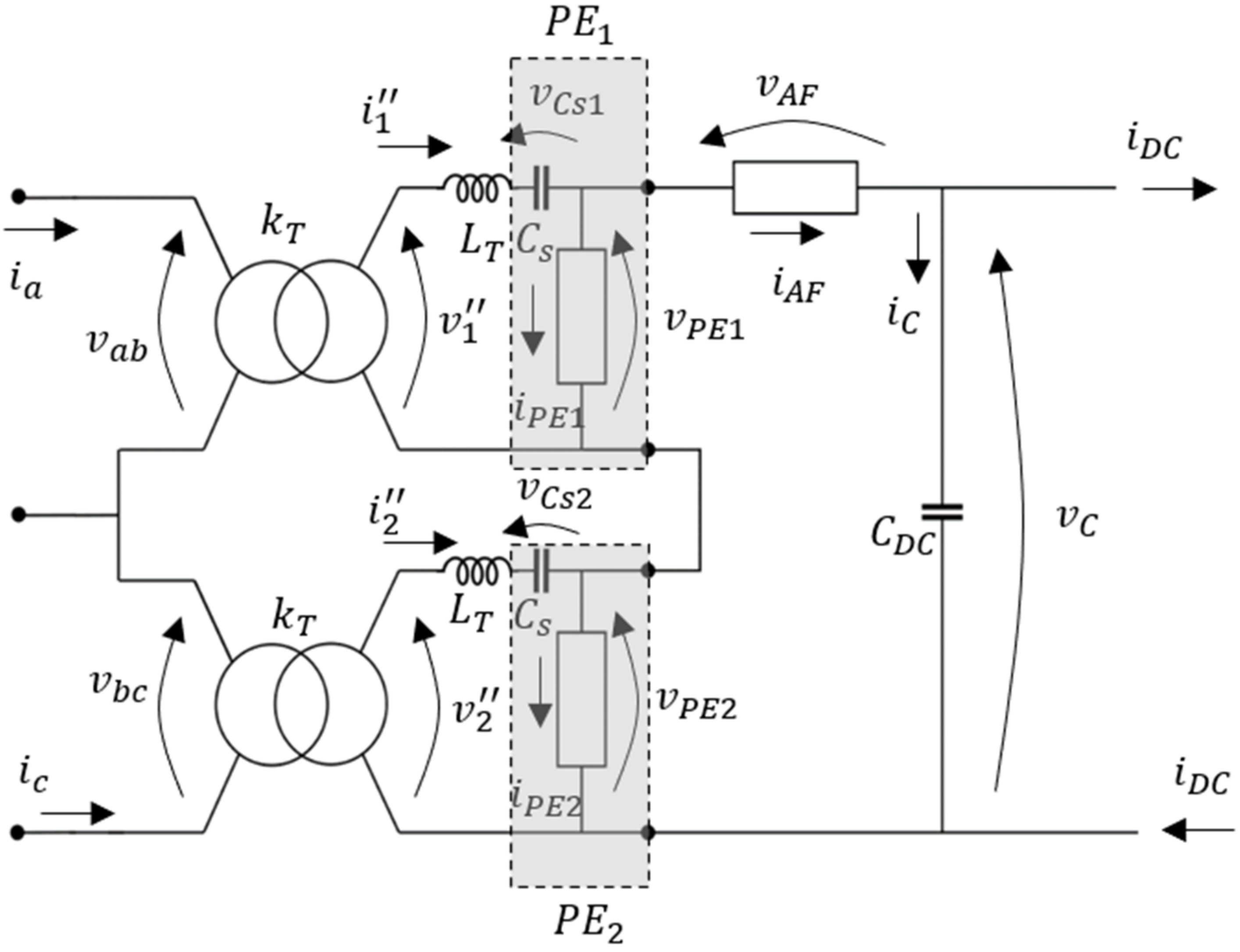
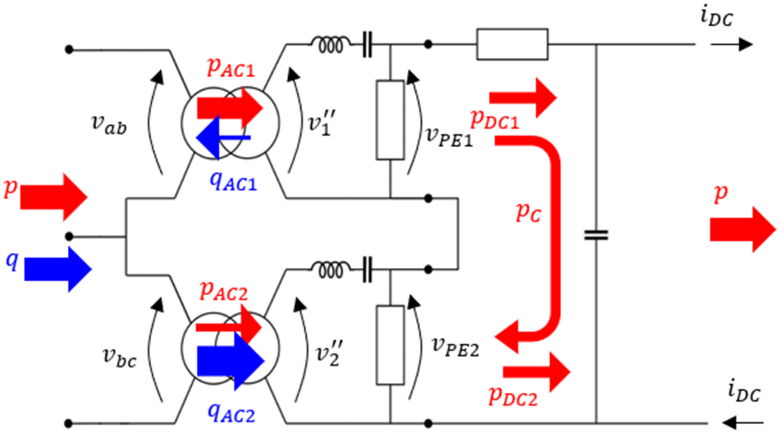
The open-delta CLSC converter topology is shown in Figure 7. It consisted of two transformers, two phase elements (PEs) comprising a SM stack and the series capacitor , an active filter (AF) (which was an SM stack), and the DC-link capacitor . The only nonphysical components in the schematic are the reactors, which represent the transformer leakage inductance.
The open-delta CLSC converter adopted the same PEs of the three-phase CLSC [27]; however, the transformers were connected following the open-delta scheme [21]. This converter belongs to family of the converters whose PEs are connected in series, such as the SBC [22,28] or the converter presented in [15], but only two single-phase transformers were employed. In order to create a symmetric and balanced load/generator from the grid standpoint, the current and voltage had to be properly controlled by the two phase elements.
This topology had the advantage of using only two transformers and no arm inductors but it was not possible to verify at first glance how it compared with a state-of-the-art MMC regarding other KPIs: even if there were only two phase elements, the number of submodules and switches could not be immediately found; in addition, it was not obvious how the submodules’ ratings compared with those of the MMC. Those considerations paved the way for the analysis of this new topology via the procedure outlined in this paper. The resulting KPIs were then compared with the ones from the MMC.
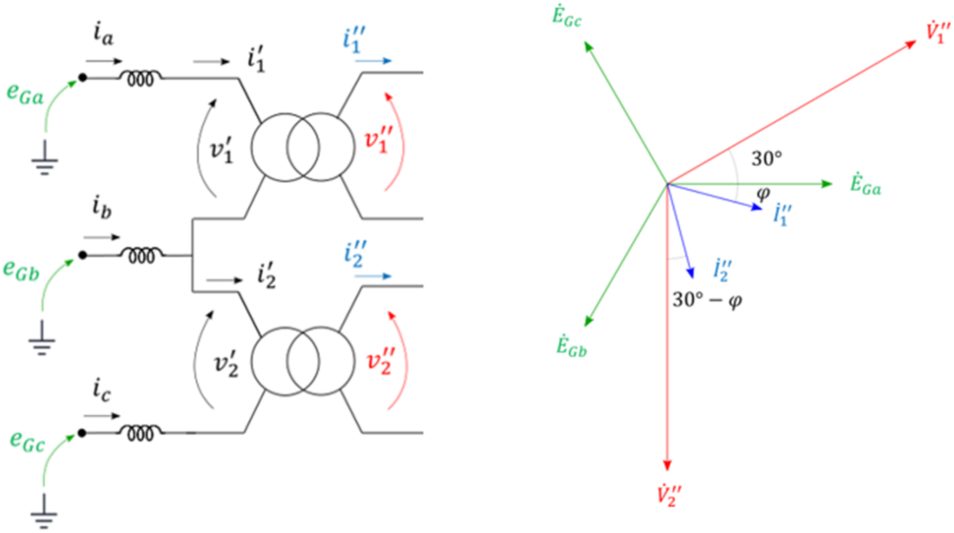
In order to form a symmetric and balanced three-phase system, the open-delta current and voltage vector diagram must be the one shown in Figure 8. In particular, the converter control must always ensure that:
It appeared that the phases carried the same amount of active power only when the reactive power was zero (i.e., when ).
It was verified that:
where , and are the active and reactive power flowing through phases 1 and 2, respectively, as shown in Figure 9. In general, since , then ; and since the average values of and were equal to , then an additional flow transferring power from PE1 to PE2 (or vice-versa) had to arise in order to maintain the energy balance in the phase elements. Such additional power flow, which can be called “circulating power flow” ( in Figure 9), was controlled by an appropriate voltage injection from the active filter (AF). Finally, the sizing of the DC-link capacitor was uniquely determined by the max acceptable voltage ripple on the DC side.
Equation Definition
The following assumptions were made:
- The series connection of the capacitor and the transformer inductance determined a perfect series-resonance.
- An ideal DC current source.
With reference to Figure 7, the characteristic equations of the open-delta CLSC converter are the following:
where is defined in (20), and in (21).
where is the transformation ratio. It could be easily verified that the voltage that had to be injected by the AF in order to be in an energy-balanced operating condition and that guaranteed the Pes’ energy balance at the same time is:
where is the maximum zero to peak voltage ripple on the DC capacitor and is the maximum reactive power in PU. Therefore, the DC side voltage can now be written as:
It is interesting to note when using (31) that no voltage ripple appears when , which is also in accordance with what is stated by Equation (27). In other words, when the reactive power was zero, there was no power circulation between the Pes, and thus no voltage ripple on the DC side. Indeed, the current flowing through is:
where:
being:
Again, using (32), it is possible to observe that no current flows in the DC-link capacitor when . Figure 10 depicts the current and voltage phasors involved in the power circulation between the PEs.
All the remaining equations can be found straightforwardly. The voltage on the series capacitors is defined in (35):
The current flowing through the PEs and the AF is defined in (36):
Finally, remembering that only half of the installed switches conducted the current at the same time, then the conduction current losses can be calculated using (37):
where and represent the number of PE and AF installed switches, respectively. The same switch chosen for the MMC was utilized here for the power-loss computation [29].
5. Sizing Results
The sizing results obtained following the outlined procedure are shown in this section as a function of . Table 1 reports the numerical values of the main parameters: the extreme and values were chosen to be and , respectively.
For calculation of the conduction power losses, the 5SNA 1800G330400 HiPak IGBT module was adopted; its datasheet can be found in [29].
5.1. MMC
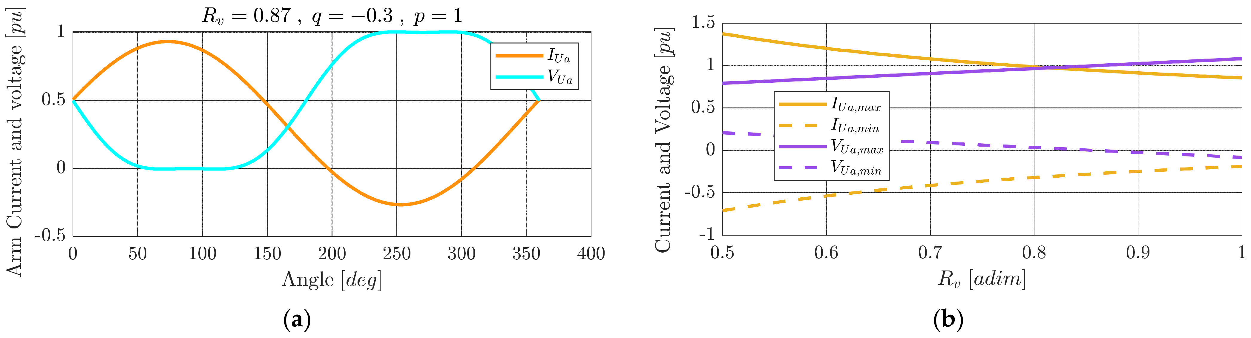
Figure 11a shows the voltage and the current waveforms for the upper arm connected to the phase a in one particular working condition. In the voltage waveform, it is possible to notice the third harmonic injection. Figure 11b, on the other hand, shows the maximum arm voltage and current as a function of the transformer secondary side voltage. It can be observed that the max arm voltage increased linearly with , as this parameter was proportional to the secondary side voltage of the transformer; consequently, the maximum current was proportional to .
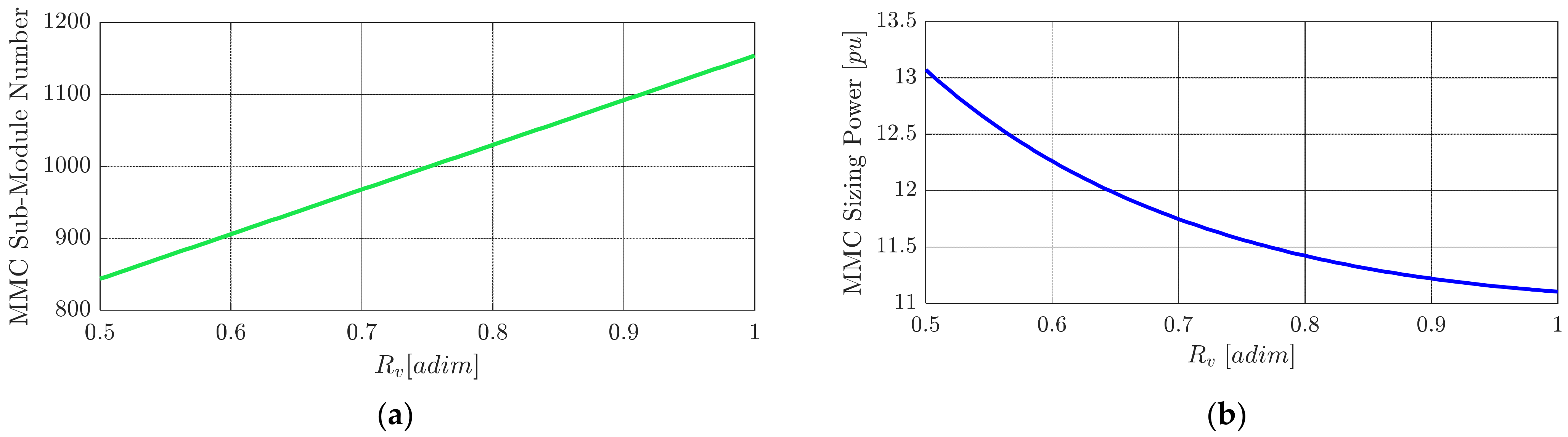
The total number of submodules and the total switch sizing power can be observed in Figure 12a,b, respectively. Again, it can be observed that the SM number increased linearly with as expected, while the sizing power slowly decreased. Assuming that only half-bridge (HB) SMs were present, then the total switch number could be obtained by simply multiplying the SM number by 2.
Figure 13a shows the dependence of the SM capacitance on , while the energy stored in the MMC while also taking into account the arm inductors is shown in Figure 13b.
It can be seen that for the MMC, there was no obvious optimum value for the . Therefore, to minimize the losses of the converter, it was chosen to be the maximum possible value. For an HB MMC, the peak of the secondary phase to ground voltage had to be below Vdc/2 to ensure the controllability of the converter. Therefore, was chosen, where the subscript “N” means “nominal”.
Once the nominal was chosen ( in this case), then all the KPIs could be computed. The KPI values are presented in the final section, where they are also compared to those of the open-delta CLSC converter.
5.2. Open-Delta CLSC
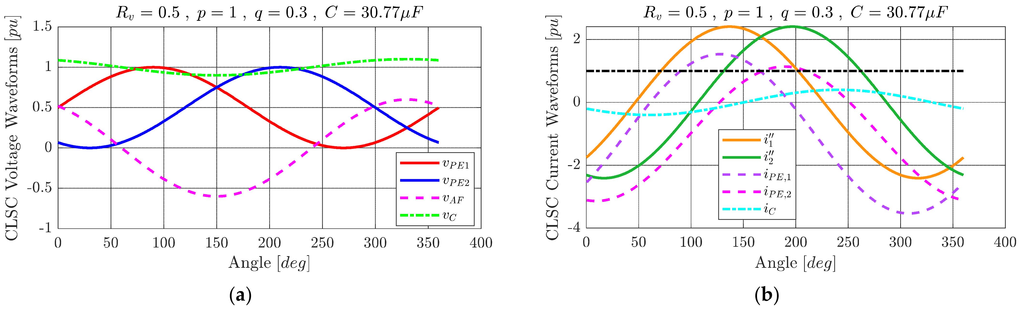
The sizing results obtained by following the outlined procedure are shown in this section as a function of . The max zero to peak DC voltage ripple was set to be equal to 0.1 PU. The current and voltage waveforms are shown in Figure 14 for a specific working condition. With reference to Figure 14, since , the sum determined a voltage waveform characterized by a nonzero mean value and a certain ripple that can be seen in . Therefore, the AF was responsible for the power exchange between PEs, as shown by Equations (30) and (31).
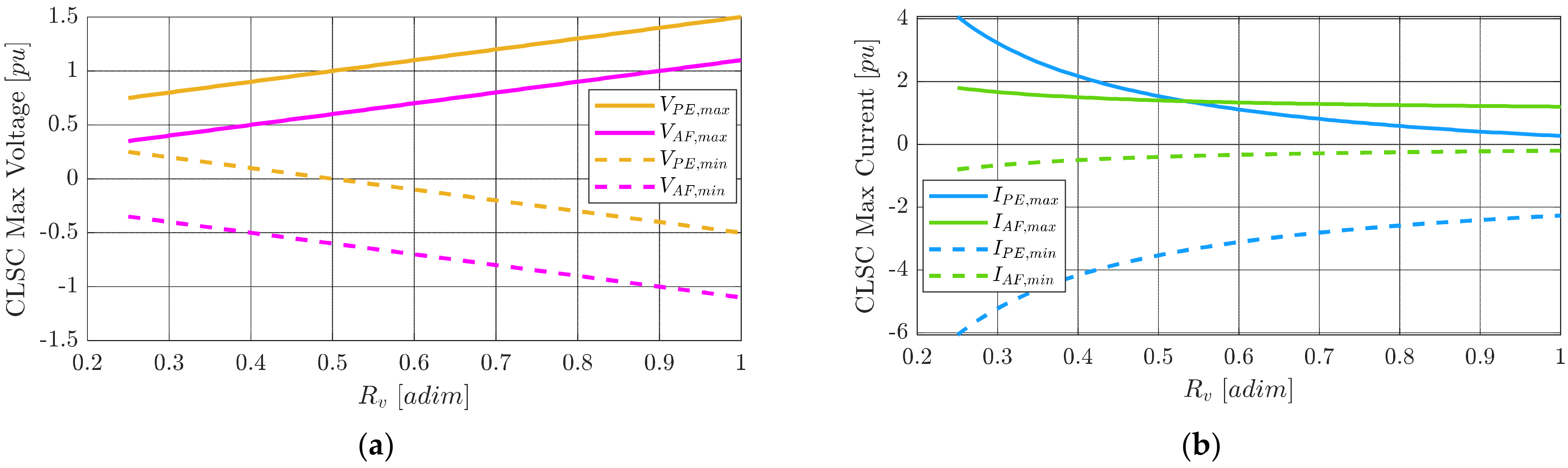
The maximum and minimum currents flowing through the converter stacks are shown in Figure 15. Again, it can be noticed that the max and min voltages increased linearly with while the maximum and minimum currents were proportional to . Additionally, a DC component was noticeable in the PE voltages, PE currents, and AF current.
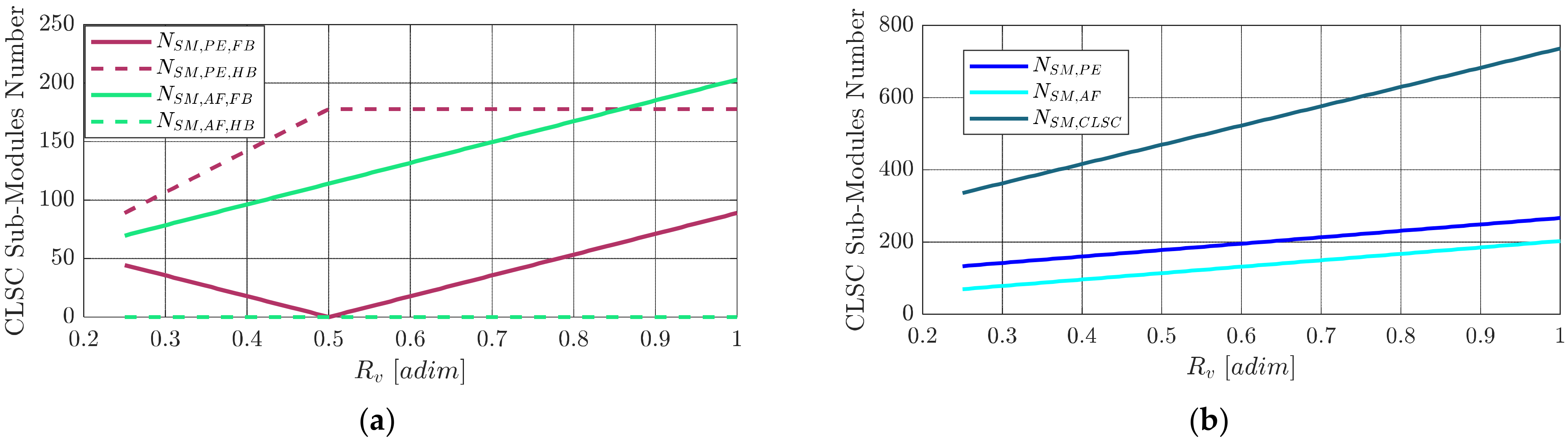
The total SM number and the SM number divided by type and stack are shown in Figure 16.
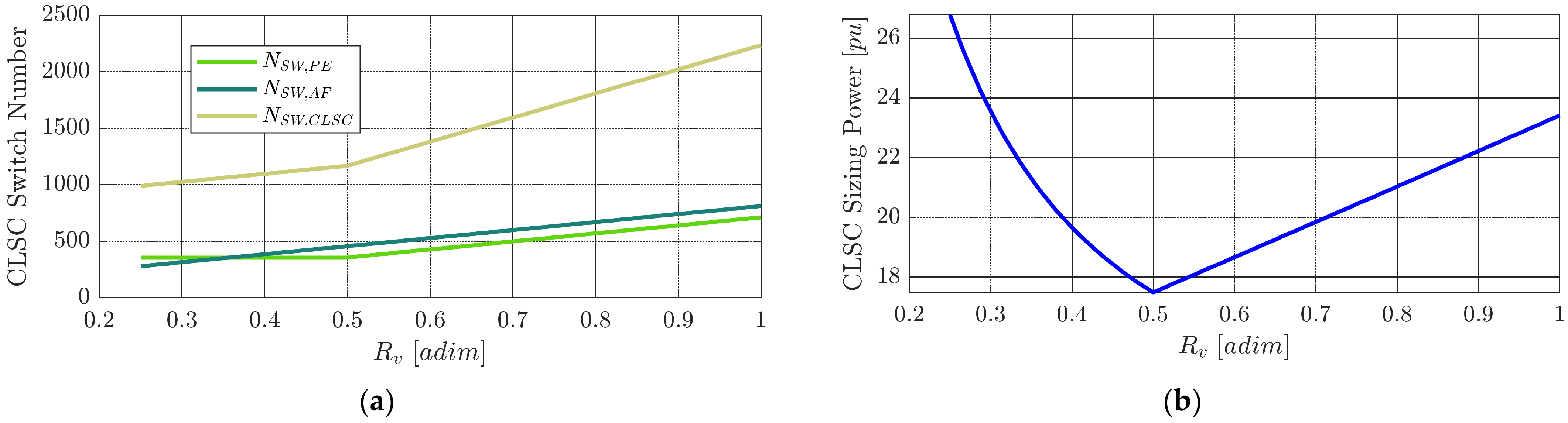
The switch number and the total switch sizing power are reported in Figure 17. Firstly, we immediately noticed the presence of a minimum point at . This was explained by the fact that, as increased above 0.5, the number of FB SMs increased, resulting in an increase in the number of switches, and therefore in the sizing power at the same time. Secondly, the sizing power curve was quite “steep” as a function of , and therefore was strongly dependent on the transformer secondary side voltage (which was not the case for the MMC, see Figure 12b). This underlined the importance of exploring the converter sizing as a function of the available degrees of freedom ( in this case).
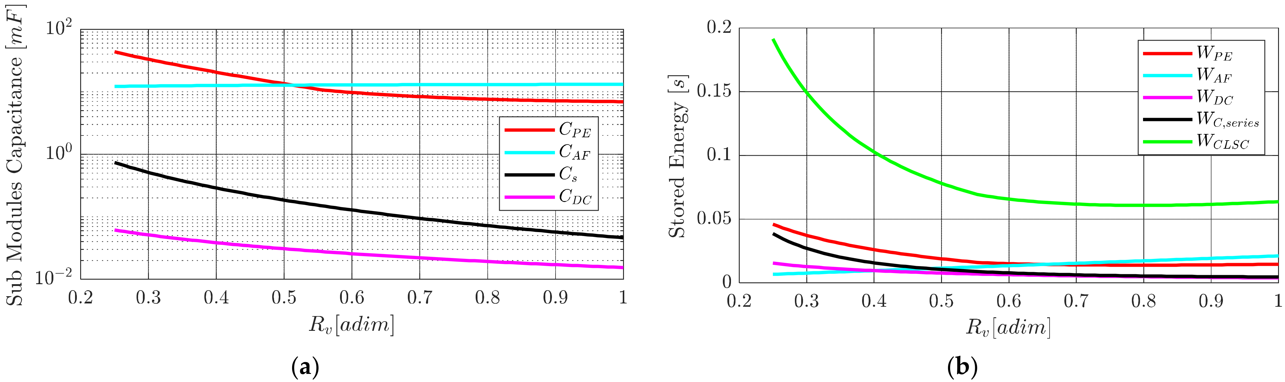
The SM capacitance and the converter’s stored energy are shown in Figure 18.
6. KPI Comparison
This section presents a comparison between the KPIs of the two converters identified thanks to the procedure outlined above. Two cases were studied in order to show the importance of the required operating domain in the converter sizing. More specifically, the KPIs of the two converters derived from a rectangular PQ domain and the line domain were compared.
In order to compute the KPIs, the degree of freedom must be fixed. It was already pointed out in Section 5.1 that for the MMC, the choice was ; however, since the open-delta CLSC is a new topology, the choice is up to the designer. In Figure 16, Figure 17 and Figure 18, it can be noticed that was a good operating point, not only because it corresponded to the minimum sizing power, but also because it was associated with a low SM and switch number, and it was close to the minimum stored energy point. The KPIs could then be obtained simply by selecting the values in the plots shown in Section 5.1 and Section 5.2 that corresponded to the chosen .
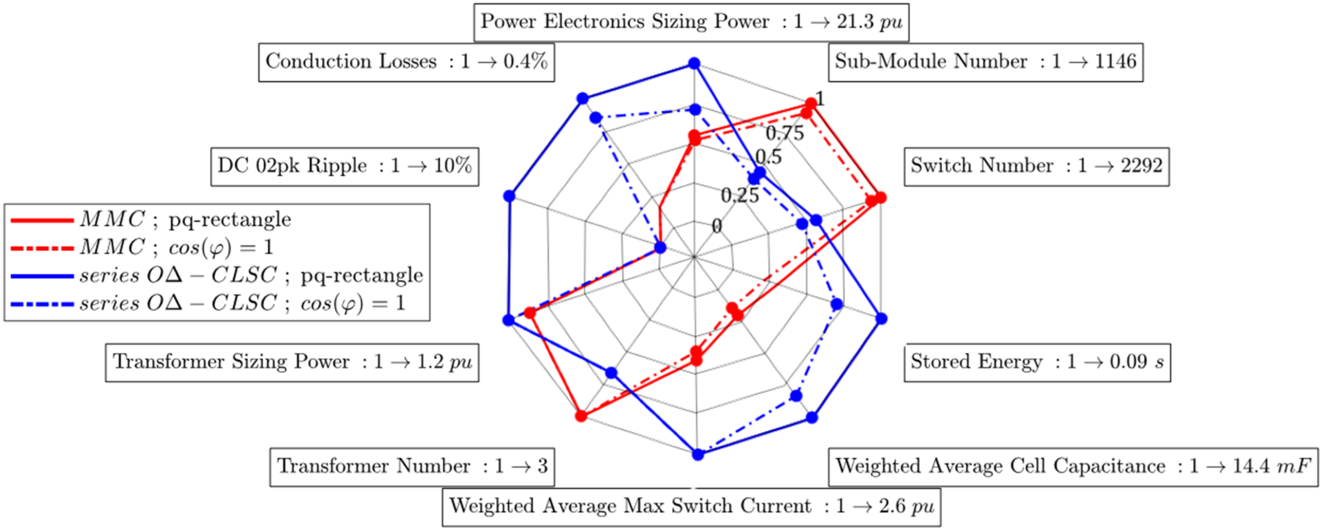
Those KPIs were collected in the spider plot shown in Figure 19 in order to compare the two converters. For a better representation, each KPI belonging to the same type was normalized with respect to their maximum, so that the external perimeter was always equal to 1, and their difference was relative.
It can be easily observed that although the MMC had a larger SM and switch number, it had a much lower sizing power, stored energy, and SM capacitance. This was mainly because the SMs in the open-delta CLSC were significantly larger than in the MMC. This can be seen in both the weighted average capacitance and the weighted average current. The necessity of creating these weighted average quantities resulted from the fact that the open-delta CLSC had two different types of SM stacks (in PEs and in AF) that were of different ratings, while the MMC was composed of six identical stacks. Therefore, in order to be able to compare the SM max current and capacitance with the MMC, it was useful to define the following quantities for the open-delta CLSC:
where and are the weigthed average capacitance and max switch current, respectively.
In Figure 19, it can be seen that the MMC was far less sensitive to the choice of the operating domain than the open-delta CLSC. As a matter of fact, the blue perimeter shrank significantly when passing from the rectangular domain to the line, while the red polygon associated with the MMC remained almost unchanged. This fact underlined the importance of clearly defining the application’s PQ domain. As an example, if a DC fault-blocking capability is required from the converter, the difference in terms of sizing parameters becomes smaller, especially the switch sizing power. The DC fault-blocking capability consists of the ability of the converter to block faults on the DC side by applying, thanks to the SM capacitors, a sufficiently high voltage of the opposite polarity [30]. The max voltage available depends on the number of FB SMs in the short-circuit current path; HB SMs are not able to counteract the fault, as they cannot change the voltage polarity at their terminals. While the open-delta CLSC had a sufficient number of FB SMs to block the max DC short-circuit current, at least 50% of the HB SMs had to be replaced by FB SMs in the MMC. This SM replacement increased the switch number and therefore the MMC switch sizing power.
7. Conclusions
A new methodology to assess the benefits of a modular converter was described in this paper. The methodology allows quick informed decisions to be made regarding whether research into a new topology should be pursued further in the early stages of development. The particular strengths of this methodology are that setting up dynamic simulations and development of the converter’s control-system design are not required, resulting in significant time savings. A rapid analysis of all the possible work points inside a prescribed PQ operating domain allows assessment of the converter sizing and evaluation of critical KPIs. Unless a significant improvement in one of the KPIs is shown, there is very little probability that the new topology will find success in practical applications, and further research into it should be stopped.
To demonstrate an application of the proposed methodology, it was applied to two HVDC converter topologies in order to investigate the potential of a candidate challenger (the open-delta CLSC) as compared to a reference in the VSC HVDC domain (the half-bridge MMC). For each topology, the steady-state equations, the PQ operating domain, and the degrees of freedom were defined; and the converter sizing, together with the critical KPIs, were calculated. The KPIs extracted from the two converters showed their differences in terms of their “sizing performance”, and highlighted their dependencies on the prescribed PQ operating domain (the MMC sizing was slightly affected by the PQ diagram, contrary to the open-delta CLSC). This not only enabled a quick quantification of the advantages related to the open-delta CLSC (reduced numbers for submodules and switches), but also the identification of its drawbacks (sizing power, switch current ratings, and stored energy). Overall, this case study indicated that the new open-delta topology did not represents a valid alternative to the classic MMC solution.
The procedure developed in this paper is valid for modular multilevel converters, as they produce voltage waveforms with a low harmonic content and can be accurately modeled analytically by ideal waveforms. Future works will investigate the generalization of the proposed procedure to converters that are not of the modular multilevel type.
Author Contributions
Conceptualization, D.L., F.M. and P.-B.S.; methodology, D.L., F.M., P.-B.S. and K.V.; software, D.L.; validation, D.L. and F.M.; formal analysis, D.L., F.M., P.-B.S. and K.V.; investigation, D.L., F.M., P.-B.S. and K.V.; resources, F.M. and P.-B.S.; writing—original draft prepa ration, D.L.; writing—review and editing, F.M., P.-B.S. and K.V.; visualization, F.M., P.-B.S. and K.V.; supervision, F.M., P.-B.S. and K.V. All authors have read and agreed to the published version of the manuscript.
Funding
This work was supported by a grant overseen by the French National Research Agency (ANR) as part of the “Investissements d’Avenir” Program ANE-ITE-002-01.
Institutional Review Board Statement
Not applicable.
Informed Consent Statement
Not applicable.
Data Availability Statement
The study did not report any data.
Conflicts of Interest
The authors declare no conflict of interest.
References
- Bahrman, M.P.; Johnson, B.K. The ABCs of HVDC transmission technologies. IEEE Power Energy Mag. 2007, 5, 32–44. [Google Scholar] [CrossRef]
- Bresesti, P.; Kling, W.L.; Hendriks, R.L.; Vailati, R. HVDC connection of offshore wind farms to the transmission system. IEEE Trans. Energy Convers. 2007, 22, 37–43. [Google Scholar] [CrossRef]
- Qin, X.; Zeng, P.; Zhou, Q.; Dai, Q.; Chen, J. Study on the development and reliability of HVDC transmission systems in China. In Proceedings of the 2016 IEEE International Conference on Power System Technology (POWERCON), Wollongong, Australia, 28 September–1 October 2016; pp. 1–6. [Google Scholar]
- Xie, H.; Bie, Z.; Li, G. Reliability-oriented networking planning for meshed VSC-HVDC grids. IEEE Trans. Power Syst. 2018, 34, 1342–1351. [Google Scholar] [CrossRef]
- Orths, A.; Hiorns, A.; van Houtert, R.; Fisher, L.; Fourment, C. The European North seas countries’ offshore grid initiative—The way forward. In Proceedings of the 2012 IEEE Power and Energy Society General Meeting, San Diego, CA, USA, 22–26 July 2012; pp. 1–8. [Google Scholar]
- Gomez, D.; Páez, J.D.; Cheah-Mane, M.; Maneiro, J.; Dworakowski, P.; Gomis-Bellmunt, O.; Morel, F. Requirements for interconnection of HVDC links with DC-DC converters. In Proceedings of the IECON 2019-45th Annual Conference of the IEEE Industrial Electronics Society, Lisbon, Portugal, 14–17 October 2019; pp. 4854–4860. [Google Scholar]
- Lesnicar, A.; Marquardt, R. An innovative modular multilevel converter topology suitable for a wide power range. In Proceedings of the 2003 IEEE Bologna Power Tech Conference Proceedings, Bologna, Italy, 23–26 June 2003; Volume 3, p. 6. [Google Scholar]
- Merlin, M.; Green, T.; Mitcheson, P.D.; Trainer, D.R.; Critchley, R.; Crookes, W.; Hassan, F. The alternate arm converter: A new hybrid multilevel converter with DC-fault blocking capability. IEEE Trans. Power Deliv. 2013, 29, 310–317. [Google Scholar] [CrossRef] [Green Version]
- Hao, Q.; Li, G.; Ooi, B. Approximate model and low-order harmonic reduction for high-voltage direct current tap based on series single-phase modular multilevel converter. IET Gener. Transm. Distrib. 2013, 7, 1046–1054. [Google Scholar] [CrossRef]
- Hao, Q.; Ooi, B.-T.; Gao, F.; Wang, C.; Li, N. Three-phase series-connected modular multilevel converter for HVDC application. IEEE Trans. Power Deliv. 2015, 31, 50–58. [Google Scholar] [CrossRef]
- Feldman, R.; Tomasini, M.; Amankwah, E.; Clare, J.; Wheeler, P.; Trainer, D.R.; Whitehouse, R.S. A hybrid modular multilevel voltage source converter for HVDC power transmission. IEEE Trans. Ind. Appl. 2013, 49, 1577–1588. [Google Scholar] [CrossRef]
- Amankwah, E.; Costabeber, A.; Watson, A.; Trainer, D.; Jasim, O.; Chivite-Zabalza, J.; Clare, J. The series bridge converter (SBC): A hybrid modular multilevel converter for HVDC applications. In Proceedings of the 2016 18th European Conference on Power Electronics and Applications (EPE’16 ECCE Europe), Karlsruhe, Germany, 5–9 September 2016; pp. 1–9. [Google Scholar]
- Patro, S.K.; Shukla, A.; Ghat, M.B. Hybrid series converter: A DC fault-tolerant HVDC converter with wide operating range. IEEE J. Emerg. Sel. Top. Power Electron. 2019, 9, 765–779. [Google Scholar] [CrossRef]
- Adam, G.P.; Abdelsalam, I.A.; Ahmed, K.H.; Williams, B.W. Hybrid multilevel converter with cascaded H-bridge cells for HVDC applications: Operating principle and scalability. IEEE Trans. Power Electron. 2014, 30, 65–77. [Google Scholar] [CrossRef] [Green Version]
- Kaya, M.; Costabeber, A.; Watson, A.J.; Tardelli, F.; Clare, J.C. A Push–Pull Series Connected Modular Multilevel Converter for HVdc Applications. IEEE Trans. Power Electron. 2021, 37, 3111–3129. [Google Scholar] [CrossRef]
- HITACHI. Static Compensator (STATCOM). Available online: https://www.hitachienergy.com/offering/product-and-system/facts/statcom (accessed on 15 June 2021).
- Schön, A.; Bakran, M.-M. Comparison of modular multilevel converter based HV DC-DC-converters. In Proceedings of the 2016 18th European Conference on Power Electronics and Applications (EPE’16 ECCE Europe), Karlsruhe, Germany, 5–9 September 2016; pp. 1–10. [Google Scholar]
- Kung, S.H.; Kish, G.J. Multiport modular multilevel converter for DC systems. IEEE Trans. Power Deliv. 2018, 34, 73–83. [Google Scholar] [CrossRef]
- Camurca, L.; Langwasser, M.; Zhu, R.; Liserre, M. Future MVDC Applications Using Modular Multilevel Converter. In Proceedings of the 2020 6th IEEE International Energy Conference (ENERGYCon), Gammarth, Tunisia, 28 September–1 October 2020; pp. 1024–1029. [Google Scholar]
- Alvarez, J.P. DC-DC Converter for the Interconnection of HVDC Grids. Ph.D. Dissertation, Université Grenoble Alpes, Greenoble, France, 2019. [Google Scholar]
- Steckler, P.-B. Convertisseur de Tension AC/DC Triphasé Comprenant Uniquement deux Modules de Conversion Electrique. EU Patent FR3112042A1, 28 April 2020. [Google Scholar]
- Farr, E.M.; Trainer, D.R.; Idehen, O.E.; Vershinin, K. The series bridge converter (SBC): AC faults. IEEE Trans. Power Electron. 2019, 35, 4467–4471. [Google Scholar] [CrossRef]
- ANGLE-DC. 2015 Electricity Network Innovation Competion. Available online: https://www.ofgem.gov.uk/2015 (accessed on 15 June 2021).
- Evans, N.; Dworakowski, P.; Al-Kharaz, M.; Hegde, S.; Perez, E.; Morel, F. Cost-performance framework for the assessment of Modular Multilevel Converter in HVDC transmission applications. In Proceedings of the IECON 2019-45th Annual Conference of the IEEE Industrial Electronics Society, Lisbon, Portugal, 14–17 October 2019; pp. 4793–4798. [Google Scholar]
- Merlin, M.; Green, T.; Mitcheson, P.; Moreno, F.; Dyke, K.; Trainer, D. Cell capacitor sizing in modular multilevel converters and hybrid topologies. In Proceedings of the 2014 16th European Conference on Power Electronics and Applications, Lappeenranta, Finland, 26–28 August 2014; pp. 1–10. [Google Scholar]
- Li, R.; Fletcher, J.E.; Williams, B.W. Influence of third harmonic injection on modular multilevel converter-based high-voltage direct current transmission systems. IET Gener. Transm. Distrib. 2016, 10, 2764–2770. [Google Scholar] [CrossRef] [Green Version]
- ABB Research Ltd Switzerland, ABB Research Ltd Sweden. AC/DC Converter with Series Connected Multicell Phase Modules Each in Parallel with a Series Connection of DC Blocking Capacitor and AC Terminals. EU Patent EP2569858B1, 1 May 2010.
- Amankwah, E.; Costabeber, A.; Watson, A.; Trainer, D.; Jasim, O.; Chivite-Zabalza, J.; Clare, J. The series bridge converter (SBC): Design of a compact modular multilevel converter for grid applications. In Proceedings of the IECON 2016-42nd Annual Conference of the IEEE Industrial Electronics Society, Florence, Italy, 23–26 October 2016; pp. 2588–2593. [Google Scholar]
- ABB. 5SNA 1800G330400 HiPak IGBT Module, Data Sheet, Doc. No. 5SYA 1471-00 11-2019. Available online: https://search.abb.com/library/Download.aspx?DocumentID=5SYA1471&LanguageCode=en&DocumentPartId=&Action=Launch (accessed on 6 November 2021).
- Judge, P.D.; Chaffey, G.; Wang, M.; Dejene, F.Z.; Beerten, J.; Green, T.C.; Van Hertem, D.; Leterme, W. Power-system level classification of voltage-source HVDC converter stations based upon DC fault handling capabilities. IET Renew. Power Gener. 2019, 13, 2899–2912. [Google Scholar] [CrossRef] [Green Version]
Figure 1.
Topology assessment methodology.

Figure 2.
Typical PQ domains for grid-connected converters: (a) rectangular profile; (b) butterfly profile; (c) reactive power only; (d) zero-Q load.
Figure 2.
Typical PQ domains for grid-connected converters: (a) rectangular profile; (b) butterfly profile; (c) reactive power only; (d) zero-Q load.

Figure 3.
General submodule stack consisting of both HB and FB SMs.

Figure 4.
Collector current–collector emitter voltage curves for the IGBT (left); forward current–forward voltage curves for the associated freewheeling diode (right).
Figure 4.
Collector current–collector emitter voltage curves for the IGBT (left); forward current–forward voltage curves for the associated freewheeling diode (right).

Figure 5.
Modular multilevel converter.

Figure 6.
MMC arm energy variation over the period in 25 different PQ work points.

Figure 7.
Open-delta CLSC converter.

Figure 8.
Open-delta phasor diagram.

Figure 9.
Series open-delta CLSC power flows.

Figure 10.
Open-delta CLSC PE and AF phasor diagram.

Figure 11.
Upper a arm current and voltage waveforms at p = 1, q = −0.3, Rv = 0.866 (a); max and min arm voltage and current (b).
Figure 11.
Upper a arm current and voltage waveforms at p = 1, q = −0.3, Rv = 0.866 (a); max and min arm voltage and current (b).

Figure 12.
MMC submodule number (a); MMC total switch sizing power (b).

Figure 13.
MMC submodule capacitor (a); MMC total stored energy (b).

Figure 14.
Open-delta CLSC voltages (a); and currents (b) for , and .

Figure 15.
Open-delta CLSC max and min voltages (a), and max and min currents (b).

Figure 16.
Open-delta CLSC SM number divided by type (a), and divided by stack (b).

Figure 17.
Open-delta CLSC switch number (a), and total switch sizing power (b).

Figure 18.
Open-delta CLSC SM capacitors (a), and stored energy (b).

Figure 19.
KPI spider plot. The notation “” means that 1 in the spider plot corresponds to the value .
Figure 19.
KPI spider plot. The notation “” means that 1 in the spider plot corresponds to the value .


Table 1.
Parameter numerical values for both of the converters.
| Name | Symbol | Value |
|---|---|---|
| DC voltage | ||
| Rated power | ||
| Max reactive power | ||
| Transformer impedance | ||
| IGBT collector–emitter forward voltage | ||
| Freewheeling diode forward voltage | ||
| IGBT on resistance | ||
| Freewheeling diode forward voltage |
Publisher’s Note: MDPI stays neutral with regard to jurisdictional claims in published maps and institutional affiliations. |
© 2022 by the authors. Licensee MDPI, Basel, Switzerland. This article is an open access article distributed under the terms and conditions of the Creative Commons Attribution (CC BY) license (https://creativecommons.org/licenses/by/4.0/).
Share and Cite
MDPI and ACS Style
Lanzarotto, D.; Morel, F.; Steckler, P.-B.; Vershinin, K. Rapid Evaluation Method for Modular Converter Topologies. Energies 2022, 15, 3492. https://doi.org/10.3390/en15103492
AMA Style
Lanzarotto D, Morel F, Steckler P-B, Vershinin K. Rapid Evaluation Method for Modular Converter Topologies. Energies. 2022; 15(10):3492. https://doi.org/10.3390/en15103492
Chicago/Turabian StyleLanzarotto, Damiano, Florent Morel, Pierre-Baptiste Steckler, and Konstantin Vershinin. 2022. "Rapid Evaluation Method for Modular Converter Topologies" Energies 15, no. 10: 3492. https://doi.org/10.3390/en15103492
Note that from the first issue of 2016, this journal uses article numbers instead of page numbers. See further details here.