1. Introduction
Particulate matter (PM), also known as particle pollution, is a complex mixture of microscopic particles and liquid droplets that get into the air [
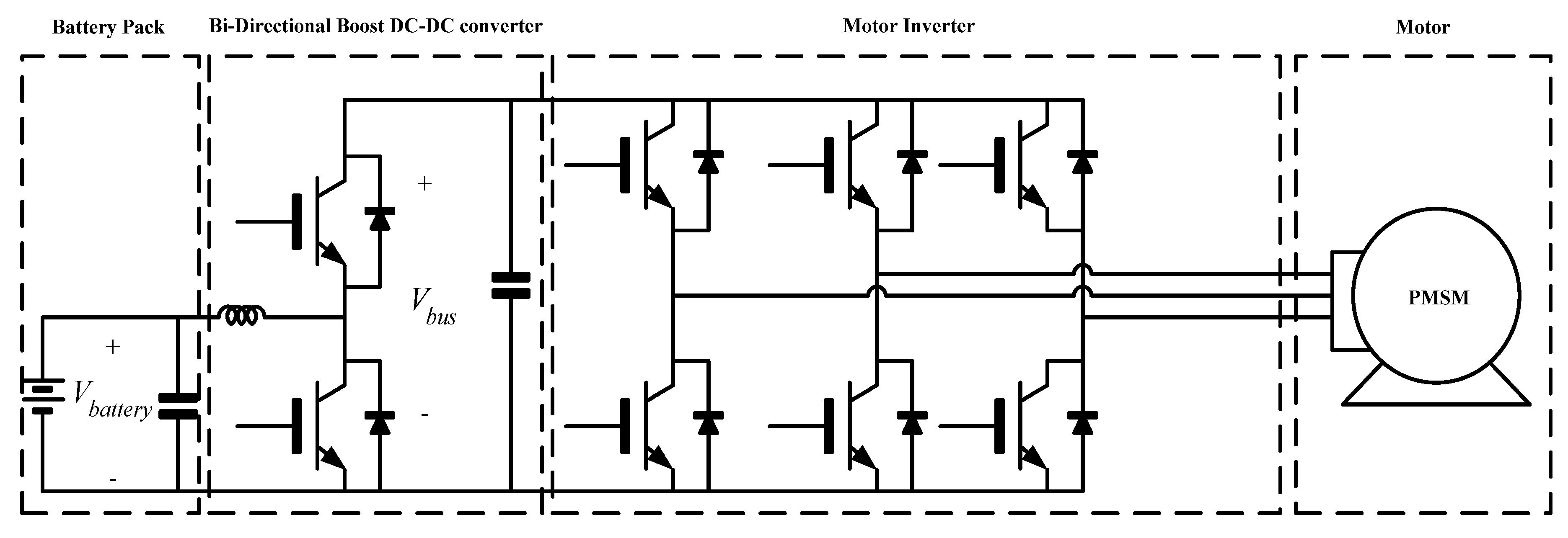
1]. This leads to health concerns that directly or indirectly affect the heart, lungs and simultaneously cause other diseases. The chemical industries and conventional vehicles significantly contribute to these health concerns. The global energy crisis and health hazards caused due to the traditional internal combustion engine (ICE)-based vehicles have led electric vehicles (EVs/automated vehicles) to become an attractive alternative solution for automotive industries/electronics. EVs outranked conventional ICE owing to non-consumption of fossil fuels and are useful to mitigate PM issues to a greater extent. The electric car is a cost-effective and electrically propelled motor-drive system which utilizes alternate energy sources on-board within the vehicle to meet zero-emission. Besides, an electric vehicle connected with different communication systems that enable its connection to external devices, networks, applications, and services is referred to as a connected vehicle. The term “connected vehicle” covers not only a variety of connections but also applications and services. This type of vehicle is not only connected to a network (vehicle to network, or V2N), they are also able to exchange information with other vehicles (V2V), with infrastructures (V2I), or even with pedestrians (V2P). Beyond their connectivity, some vehicles can integrate more or less significant levels of driving assistance. In extreme, autonomous vehicles are capable of driving without the driver’s intervention in specific configurations. These automated vehicles require a high-end communication aspect. Thus, this survey has been categorically split into two parts based on various technical viewpoints. An EV is formed by the integration of a different set of technologies working together to develop a complete electric machine. The machine can compete for conventional vehicles in the future in the sense of driving range, wide operating speed, high power density (in terms of circuit volume inside EV), high-level communications, and least emission. The next level of EVs will also include automated vehicles, connected vehicles, hybrid electric vehicles, and autonomous vehicles. This vehicle is highly interlinked with exciting and high dimensional interdisciplinary engineering technologies. The PEC is a non-linear circuit topology with an advanced control function and is useful for controlling various subsystems within the vehicle. A special class of PEC is DC-to-DC converters that are used to transfer DC power from the battery to the motor-inverter section. The schematic diagram of bidirectional converters (BDCs) is technically a sub-category of DC-DC converters and is meant to transfer energy from the battery to the motor inverter section or feedback the regenerative power to the battery is shown in
Figure 1.
EVs’ heart is utterly dependent on how power electronics technology plays a role in controlling the vehicle’s motor drive system. Simultaneously, optimally managing the on-board energy resources to propel, accelerate efficiently, and cruise may be done based on the driver needs. Advances in electric vehicles lead to various derivatives such as battery electric vehicles (BEVs), hybrid electric vehicles (HEVs), and fuel cell electric vehicles (FCEVs) [
2,
3,
4,
5]. All these derivatives have sub-categories as per the advances in EV technology. Moreover, there is a need to get acquainted with the term “vehicle-powertrain”. The powertrain of a vehicle consists of a motor-drive system and battery. In some cases, DC-DC (Bi-directional) converters are placed between the battery and motor drive system for the bidirectional power flow. Caricchi et al. [
6] reported that motor drive efficiency is severely affected if the battery system is directly feeding power to the inverter motor drive system. The bidirectional converters and communication aspects used to facilitate electric power conversion and communication with the outer environment are critical components for an automated vehicle. The power electronic bidirectional converters play an active role in transferring DC power from the battery to the motor-inverter section. Similarly, antenna technology is essential for automotive radar applications in leading the vehicles to a fully automated and autonomous state. Thus, a critical survey has been conducted on converters and communication aspects, keeping because of the future automated vehicle technology. The present article, i.e., Part 1, discusses several useful bidirectional DC-DC power converters for electric vehicle applications. The details of which are as follows: conventional bidirectional converters [
6,
7,
8,
9,
10,
11]; isolated bidirectional converters [
12,
13,
14,
15,
16,
17,
18]; soft-switching converters [
19,
20,
21,
22,
23]; coupled inductor approaches [
24,
25,
26]; fly-back converter [
27,
28]; three-level converter [
29]; dual active bridge converter approaches [
30,
31,
32,
33,
34]; and composite converter approaches [
35,
36]. From the state of the art, it has been observed that the composite converter is the most efficient power converter in which different sets of modules are connected in series or parallel to control the power flow. The conduction and switching losses are reduced by two to four times as compared to conventional topologies, which lower device stresses and hence, lowers the voltage rating of power devices. In addition, conditioning monitoring aspects for the PECs are emphasized as the concern of the life span of the power converter installed in the EV is a very crucial issue [
37,
38,
39,
40,
41,
42,
43,
44,
45,
46,
47,
48,
49,
50,
51,
52,
53,
54,
55,
56,
57,
58,
59,
60,
61,
62,
63,
64,
65,
66,
67,
68,
69,
70,
71]. The aging effect of the electric vehicle’s electronic components needs to be essentially monitored to maintain the drive system’s health. Health index monitoring is an important liaison for the power electronics hardware installed within the EVs. In part 2 of this survey, 24 and 77 GHz low-profile (microstrip-based) antennas for automotive radar applications, types of antenna structures, feed mechanisms, dielectric material requirements, design techniques, and performance parameters have been critically surveyed and reported.
2. Bi-Directional Converter Approaches
In the past few years, with the evolution of semiconductor device technology, there had been tremendous growth in the power semiconductor devices in terms of their power ratings and current handling capabilities. Efforts are still going on to enhance the issues mentioned above by changing the structure of power devices so that the device’s current flow will not result in higher conduction losses and switching losses. With the advent of the wide-band-gap devices such as silicon carbide (SiC) and gallium nitride (GaN), it is expected that the reduction in silicon area and higher switching frequency benefits. In effect, a smaller silicon die is required to implement the power device and reduce the bulky magnetics’ size due to higher switching frequency.
This section deals with the bidirectional dc-dc converter approach, which is dedicated to electric vehicles. Topologies involved in the article utilizes conventional semiconductor switches such as insulated gate bipolar junction transistors (IGBTs), metal oxide semiconductor field effect transistor (MOSFETs), and bipolar junction transistors (power BJTs) as well as the wide-band-gap devices or combination of both.
2.1. Conventional Bi-Directional Approaches
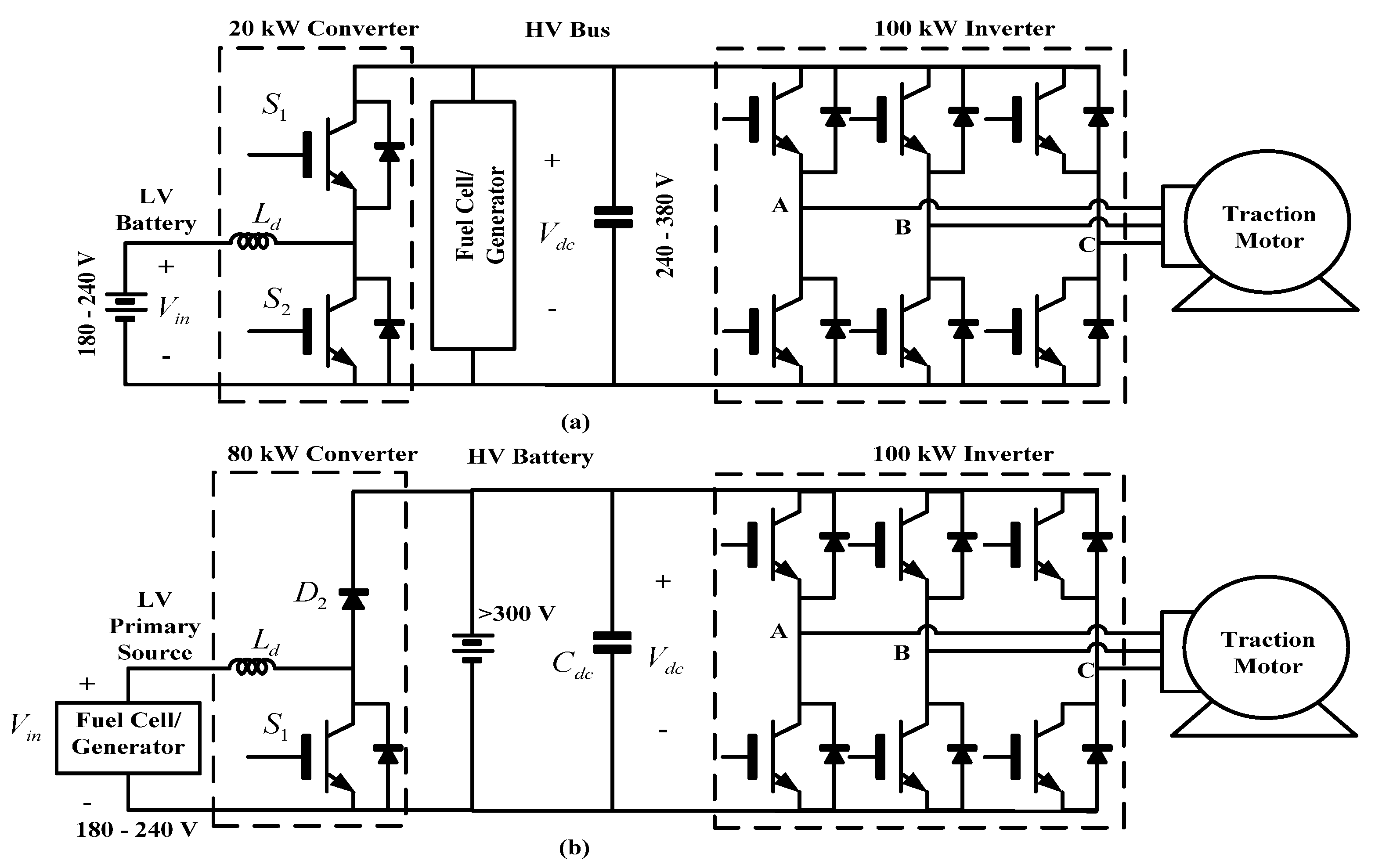
The conventional bidirectional converter is directly related to well-known non-isolated type power electronics topologies that are already matured and well explored, i.e., (1) buck, (2) boost, and (3) buck-boost converter topologies [
6]. As illustrated in
Figure 2, the two approaches, buck and boost topologies, are shown with their practical implementation for fuel cell hybrid electric powertrain. Since losses associated with these topologies are high in terms of conduction losses and switching losses, a right solution is to use a synchronous buck or synchronous boost topology. Here the power diode is replaced by controlled semiconductor devices, which in effect minimizes conduction losses associated with the power diodes to some extent. The same alternative can be applied and opted for buck-boost topology as well. A buck-boost converter [
7,
8,
9,
10,
11] is more versatile when the DC-bus voltage level is the same as the battery voltage level.
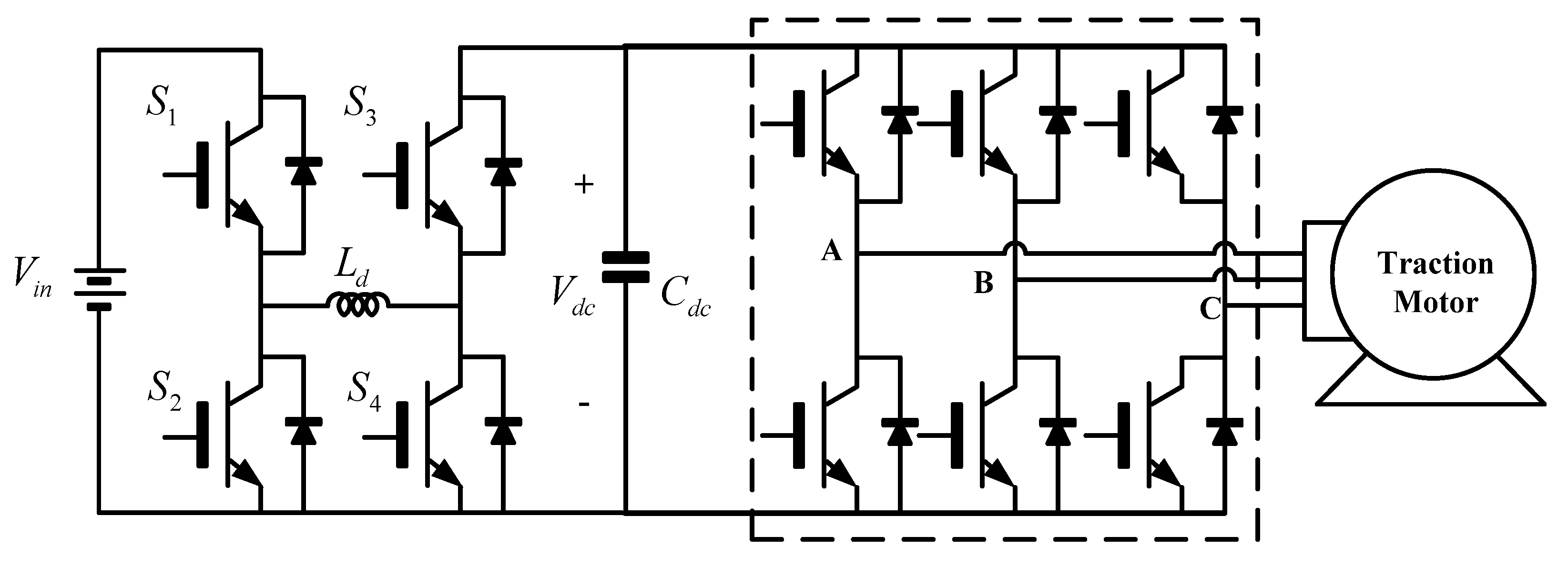
On the contrary, during normal conditions, i.e., when the battery voltage is less than the DC-bus voltage, buck or boost type converters are preferred more since fewer components are required for implementation. Cost is the primary objective in any application; therefore, boost or buck type converters are more useful to meet the desired cost objective.
Figure 3 illustrates the buck-boost topology for high power EV applications.
2.2. Isolated Bi-Directional DC-DC Converters
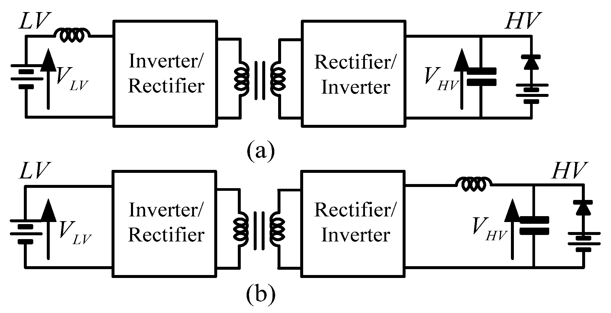
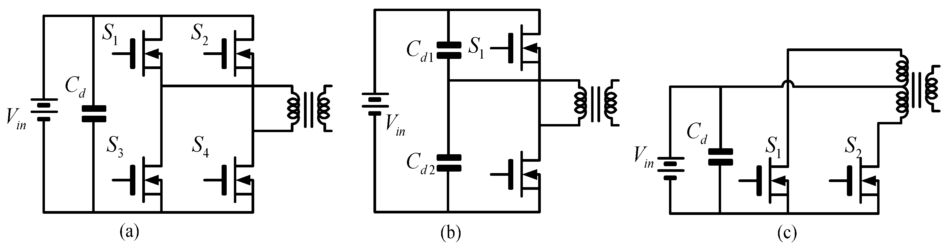
Isolated converter topologies prefer isolation utilizing a transformer, which inherently increases losses due to the transformer’s involvement in the circuit topology. Isolation becomes necessary when the negative terminals cannot be connected to the LV and HV sides’ ground together. Furthermore, when constraints arise from the fact that the device cannot handle a very high voltage and current, isolation becomes necessary. The two configurations for isolated bidirectional converters are shown in
Figure 4. For smooth power flow, a current source is introduced in between the LV side and the HV side. Therefore, two categories can be derived, i.e., voltage source converters and current source converters. They may be sub-categorized as (a) half-bridge, (b) full-bridge, (c) push-pull. To include a voltage source on any side of the configuration, a capacitor is introduced in parallel to the DC bus, or an inductor is connected in series to make it as a current source.
2.2.1. Voltage Source Converter
In the full-bridge configuration shown in
Figure 5a, complete voltage is applied to the bridge and, therefore, concerning full-bridge current stresses through the devices in half-bridge depicted in
Figure 5b is almost doubled; similarly, voltage stresses got doubled in push-pull configuration. In order to increase the power handling capability of the devices, multiple devices are connected in parallel; hence, the total silicon area needed will vary according to the configuration used. Therefore, from a designer’s point of view, one has to take care extremely of parasitics and magnetics influences since these factors contribute to significant losses in the converter. A floating gate drive issue arises in a half-bridge configuration, which can be mitigated using a push-pull converter. However, high power designs will be difficult to achieve in this scheme. To resolve the issue of using a minimum number of parallel switches, the large size of the inductor, and floating gate drive, some converters are proposed in [
12,
13,
14].
2.2.2. Current Source Converter
An isolated boost converter may be considered as a current source converter. Switches are connected in a short circuit condition for storing energy in the inductor, as in the case of the conventional boost converter. Finally, switches are opened to transfer energy via an isolation transformer to the output, as depicted in
Figure 6.
The transformer turns ratio helps improve the higher voltage demand at the output terminals, which may be stated as input voltage times the turns-ratio. A significant fact about the switches between the voltage source and current source converter is that the voltage source converter requires dead time between the turn-on of the switches. In contrast, current source converters require an overlap period between the turn-off of the switches since charging inductors overlap period is necessary. For the soft switching of converters, the phase-shift modulation (PSM) scheme is required rather than the pulse-width modulation (PWM) scheme [
14].
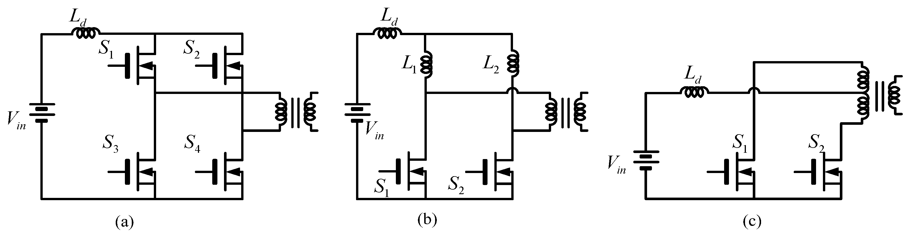
As aforementioned,
Figure 7 depicts an isolated converter for EV application, which can reduce the size by using a split inductor approach called an L-type converter. By this scheme, inductor current ripples are canceled, which enhances the battery life of the powertrain. Rc-Cc (resistor-capacitor, subscript “c” stands for clamping) clamping circuit is required to reduce LV side MOSFETs’ voltage stress during switching. To eradicate, a full-bridge type converter is proposed [
15,
16,
17,
18]. Besides, the active clamping circuit is required for reducing the voltage stress of LV side MOSFETs, as shown in
Figure 8. Active clamping allows zero-voltage zero-current switching (ZVZCS), which resets the primary side current to zero when the battery is in discharging mode as the switch Sc is turned on. Simultaneously efficiency of the converter improves with this approach. Overall efficiency over a wide load range, size, and weight is improved; however, cost concern is raised due to the clamping capacitor’s size.
2.3. Soft-Switching Approaches
Non-isolated and isolated converter approaches will further be enhanced by the soft-switching techniques, namely zero-voltage switching (ZVS) and zero-current switching (ZCS). These techniques have been extensively studied and explored by different researchers. In practice, these techniques’ major objective is to mitigate switching losses associated with a conventional boost converter. Therefore, auxiliary circuits will support soft switching at the expense of additional losses since they usually operate under hard-switching conditions. Generally, hard switching took place twice in a switching cycle [
19,
20]. However, the tradeoff between cost and efficiency is essential. Ito et al. [
20,
21] addresses the switching loss associated with turn-on diode reverse recovery, and turn-off losses are present due to IGBT current tailing. Conduction losses and devices switch stress remain the same as the conventional boost converter. Auxiliary circuits are easy to implement, as shown in
Figure 9, this topology is based on snubber assisted zero voltage/zero-current transition (SAZZ), whose efficiency reaches 96% when operating at 100 kHz using MOSFETs and SiC diodes.
Zhang et al. [
22], proposed a 100 kW prototype where ZVS is achieved at heavy load conditions. A discontinuous conduction mode (DCM) operation is used to reduce the inductor size and turn-on losses. However, turn-off losses increase when the main switch is turned off at twice the load current or higher [
23]. The concept of interleaving helps in reducing the current ripple, and interleaving may be illustrated in
Figure 10 where multiple phases are created, and separate inductors are placed in each stage to cancel out the high-switching frequency current ripple.
Soft–switching approaches are necessary for improving the efficiency of the converters. In further sections, topologies investigated will involve soft-switching strategies to meet the issues related to converter efficiency improvements.
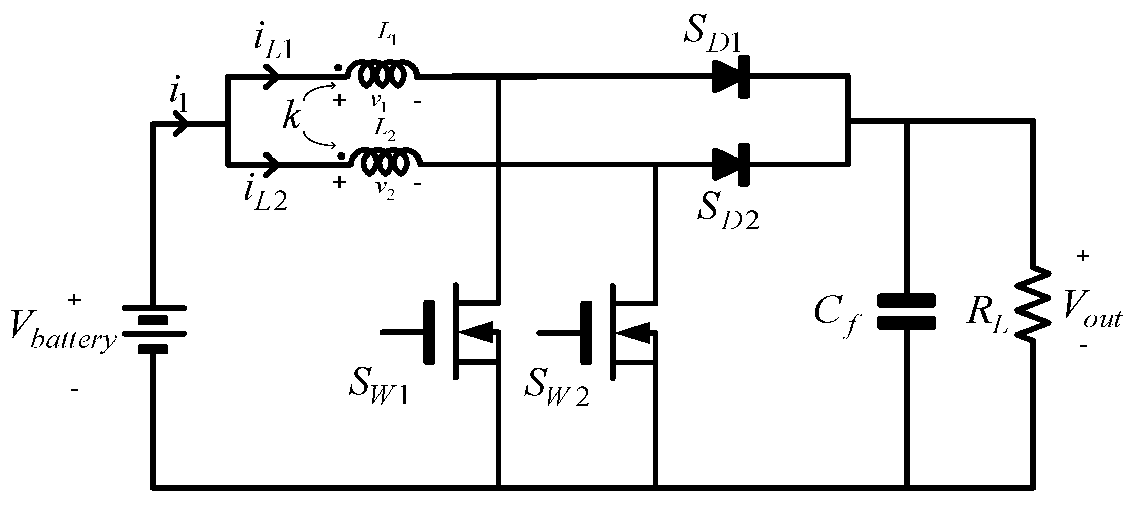
2.4. Coupled Inductor Approaches
Lee et al. [
24] proposed a boost converter that utilizes two concepts, i.e., parallel interleaving and coupled inductors are shown in
Figure 11. The primary advantage of introducing the topology is to look at it from the magnetics point of view as inductors are wound on the same core, reduction in the converter size can be achieved. As shown in
Figure 10, interleaving is taking care of ripple current reduction and increase the output current, which will again be utilized in this approach. Current sharing is very sensitive to the mismatch in the duty cycle [
25].
Therefore, current sharing among the parallel paths is a major design problem. Suppose two boost converters are connected in parallel with the same configurations and constraints about voltages and currents. In that case, the converter with a large duty cycle will operate in continuous inductor current mode (CICM). At the same time, others will work in discontinuous inductor current mode (DICM). However, further loading of the converter leads the converter to operate in CICM. The two methods contribute to significant advantages depending on the modes, i.e., in CICM: reduced conduction loss and lower input current ripples, while in DICM: lower boost rectifier reverse recovery loss and lower transistor switching-on loss. Therefore, incorporating CICM in the proposed topology reduces the inductor current ripple and peak current stresses of the inductor/switch to a lower value. As far as uneven current sharing is concerned, the inductor current flowing in the converter are discontinuous, which resolve the concerned issue. While the converter operates in DICM mode, boost reverse recovery diodes, i.e., SD1/SD2 are turned off before switches SW1/SW2 are turned on. Therefore, the need for current sensors is eliminated. Further, in
Figure 12, a new interleaved bidirectional snubber less converter approach is introduced by Xuewei et al. [
26] with an experimental prototype of 500 W (Vin = 12, fs = 100 kHz, Vo = 300 V) for fuel cell-based vehicles (FCV).
This eliminates the use of snubber circuits by utilizing the secondary modulation technique to clamp the voltage across the primary side switches naturally with zero-current commutation. Therefore, the active clamping circuit is removed, which is a significant challenge in any topology. As a result, the overall cost reduces. ZCS takes place in primary-side switches, whereas ZVS occurs in secondary side switches that help reduce switching loss. Thus, smaller magnetics and higher switching frequency can be implemented. Interleaving helps improve the converter power handling capability and the reduction in the size of passive components. Input and output filter size is reduced due to continuous current and high ripple frequency. Effects of stray inductances and capacitance in printed circuit board will bring in minor parasitic ringing; however, rated efficiency reached 93%.
2.5. Flyback Converter Approaches
Bhattacharya et al. [
27] proposed a new candidate for bidirectional power flow with multi-power-port (MPP) features, as shown in
Figure 13. It can handle multiple sources due to the modular structure. The control strategy used for voltage regulation is hysteresis control. As leakage inductance is another cause of switching losses; therefore, the proposed topology reduces the leakage inductance that, in effect, reduces the switching losses. Galvanic isolation is useful since operating boost or buck-boost converter at a very high duty ratio will not be effective as high capacitor current may be produced. One such isolated topology is the zeta-flyback converter, where an active clamp circuit helps achieve ZVS and limits the voltage stresses of the main switch [
28].
As multiple energy sources are connected in parallel, then zeta-flyback is not an optimum choice; therefore, MPP topology will improve the converter’s total energy storage capacity. When the load is very less in forwarding power flow, the converter operates in DCM (discontinuous conduction mode). Further, due to the converter’s hard switching in MPP, topology efficiency is less than soft switching topologies. However, leakage inductance reduction leads to lesser conduction and switching losses. This 6 kW MMP bidirectional flyback converter may be scaled up to increase the converter’s power handling capability by doubling and paralleling the flyback transformer’s winding at the expense of the increased core size. A soft start strategy is used to reduce the high transient current produced in the DC-link capacitor by gradually increasing the duty cycle from 0% to 75% [
28]. In the subsequent section, a new soft-starting approach is discussed.
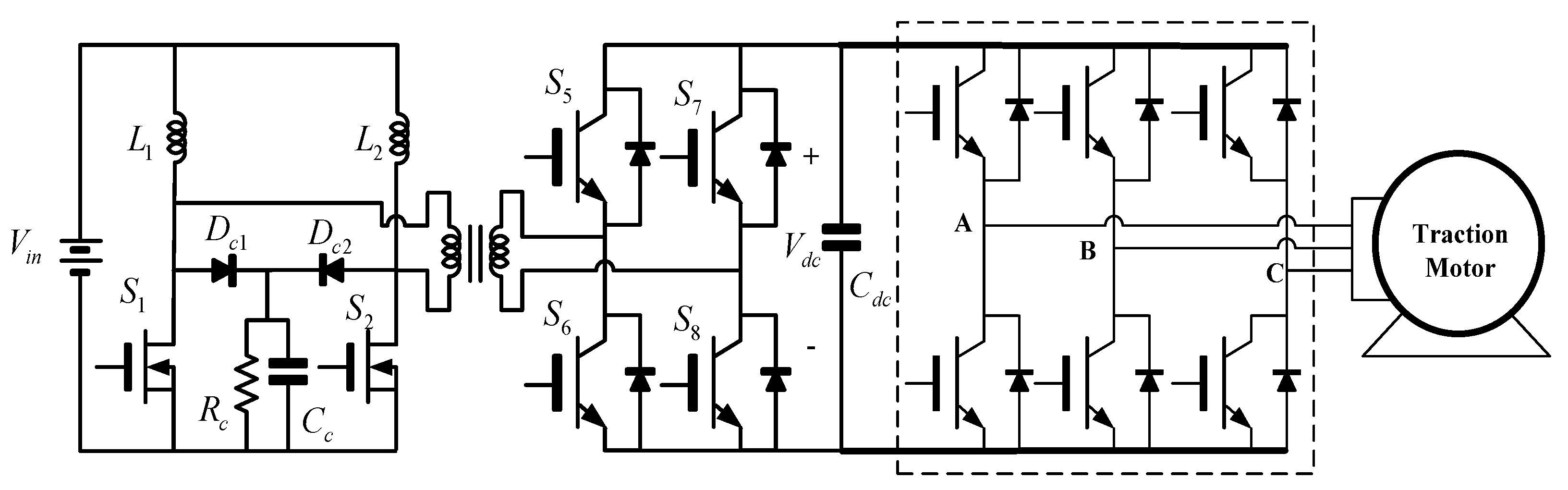
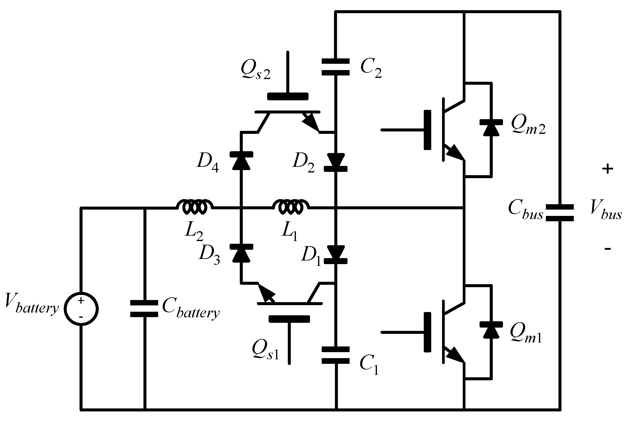
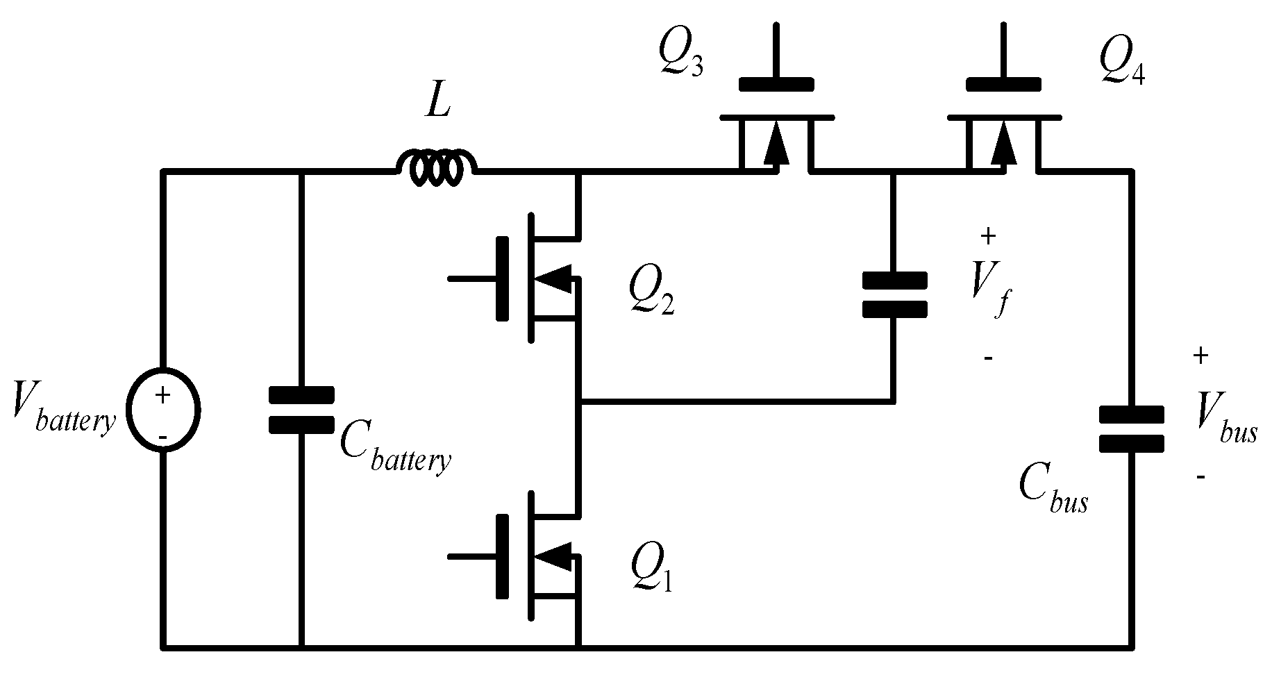
2.6. Three-Level Converter Approaches
Three-level bidirectional converter (3L-BDC), as shown in
Figure 14, is one of the prominent technologies for electric vehicles’ powertrain. Voltage stress across the device is reduced by one-half of the bus voltage, which reduces inductor volt-seconds. Hence, switching frequency is one-half of the inductor current ripple frequency that substantially minimizes the inductor size and losses. Jin et al. [
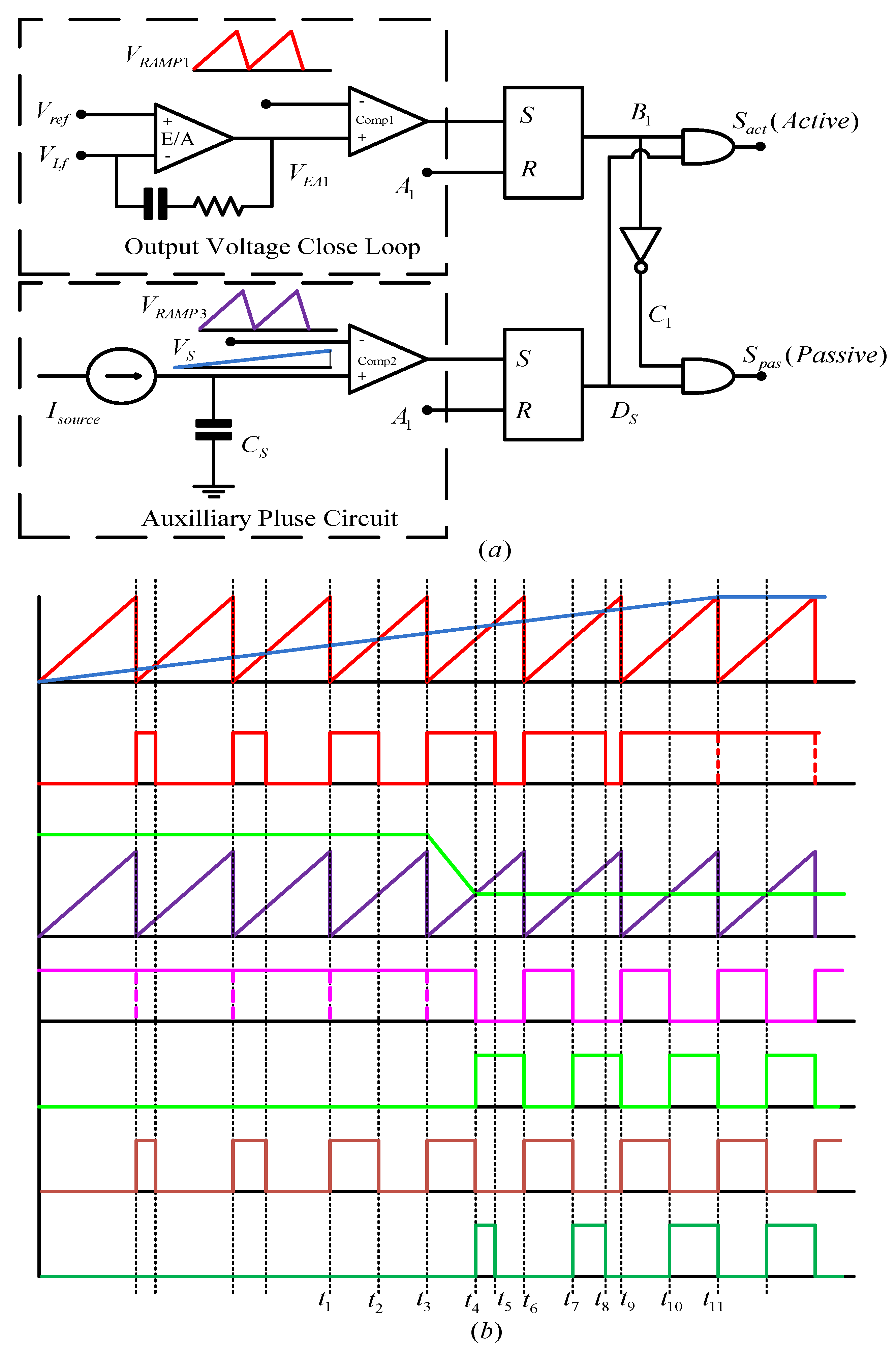
29] proposed 3L-BDC (1 kW prototype) with the benefits above. However, switching loss is not eliminated since the MOSFET body diode reverse recovery is critical and needs to be investigated in the design. Large RMS current through the flying capacitor requires a larger capacitor in a volume that affects the converter’s cost. A traditional soft-start strategy cannot be employed since a large inverse inductor current is developed in the converter. The condition for using traditional soft-start is that BDC must be introduced in between battery and load. However, for hybrid power source systems where FC (fuel cells)/battery and DC bus all act as sources on both the terminals of the BDCs, a new soft switched-circuit has been proposed by the authors to avoid the damage caused by the inverse current. For awareness, the soft-start circuit is shown in
Figure 15a, the voltage
is feedback in order to compare with the reference
. The error voltage is denoted by
which is compared with the saw-tooth voltage, i.e.,
, such that the active switch is easily controlled. On the other hand, the external capacitor
will begin to charge through the source current denoted by
, therefore,
begins to increase form zero slowly which is then compared with
to generate auxiliary pulse by employing the RS flip-flop. For further knowledge on the soft start circuitry, the details of the timing sequence
Figure 15b, i.e., from
to
is discussed in detail in [
29].
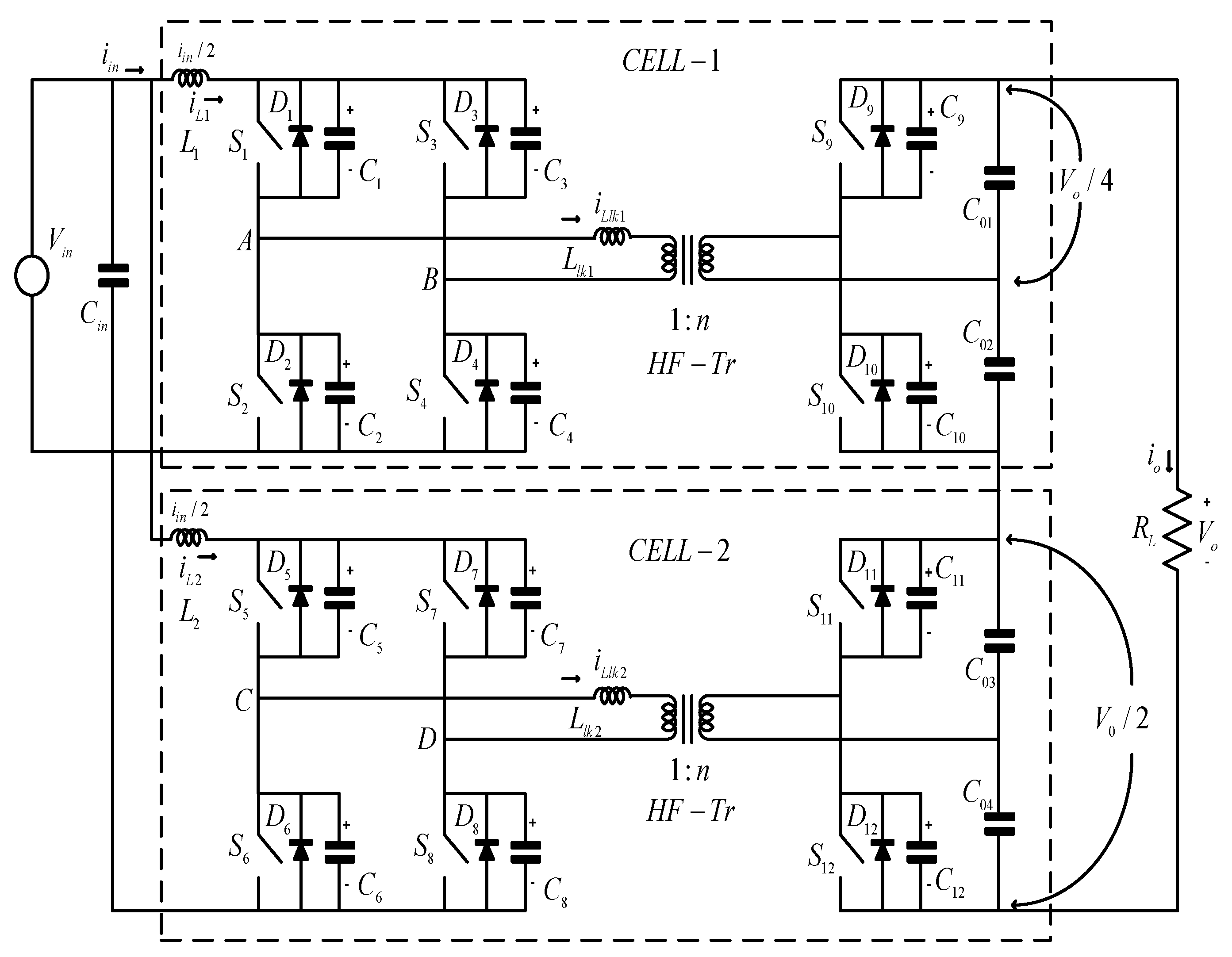
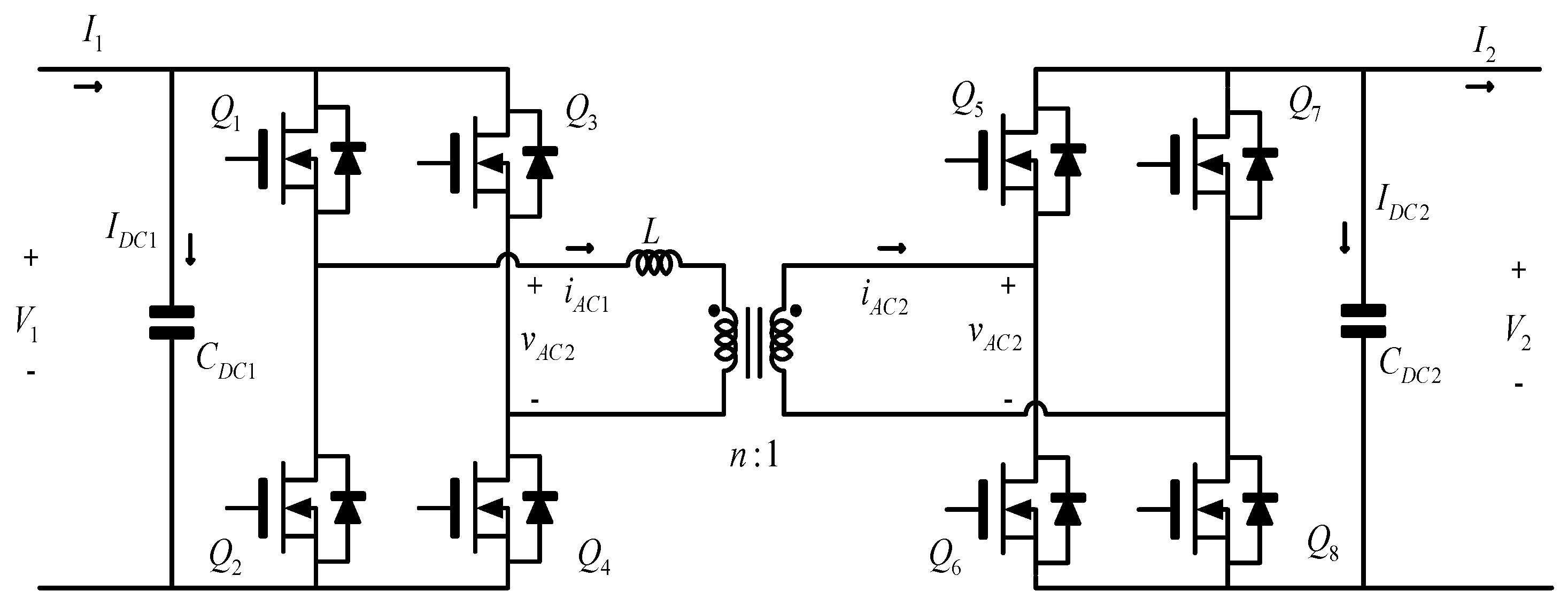
2.7. Dual-Active Bridge (Dab) Converter Approaches
Krismer et al. [
30] introduced the 1 kW prototype shown in
Figure 16, with a high current dual active bridge (DAB) which is operated at a wide voltage range based on the fuel cell vehicle application with a bidirectional interface between the battery and high voltage DC bus. High current stresses on the battery side will impact the overall efficiency of the system. Improved performance may be achieved with the sophisticated modulation concept comprising three modulation schemes: triangular, trapezoidal, and phase-shift (PS) modulation [
30,
31,
32].
Further, Krismer et al. [
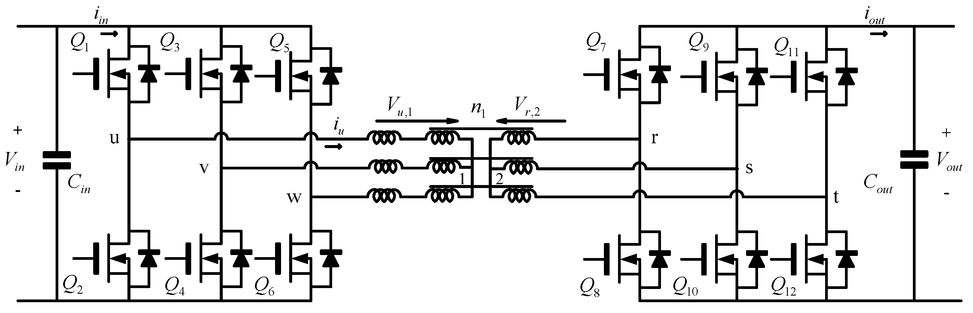
32] used the modulation schemes, such as the triangular and trapezoidal modulation schemes, and reported an improved efficiency of 2%. Although high current single-phase (1-p), DAB can meet the requirements of wide operation range and low voltage at the expense of the excessive need for filter capacitors. However, 3-p DAB (in
Figure 17) is another right candidate for the bidirectional converters.
However, the PS modulation scheme’s adoption leads to lower efficiencies for specific operating points due to hard switching [
33]. Further, they are more suitable for single operating points, but the control strategy used for 1-p DAB is more convenient and significantly improves the overall efficiency. Hoek et al. [
34] proposed the combination of triangular and trapezoidal schemes for 3-p DAB to address the poor partial load efficiency issue. When the PS modulation scheme is used for 3-p DAB, coupling occurs, and switches do not turn-off at the maximum current. Therefore, switching losses are lowered with a significant reduction in the output current ripple, which reduces the capacitor size. A critical parameter is the same silicon area used for both types of converters for converter analysis for analyzing the impact of the proposed modulation schemes on switching devices. 3-p DAB has 2/3 of the silicon area of the 1-p DAB as there are 8 switches within the 1-p DAB and 12 switches within the 3-p DAB.
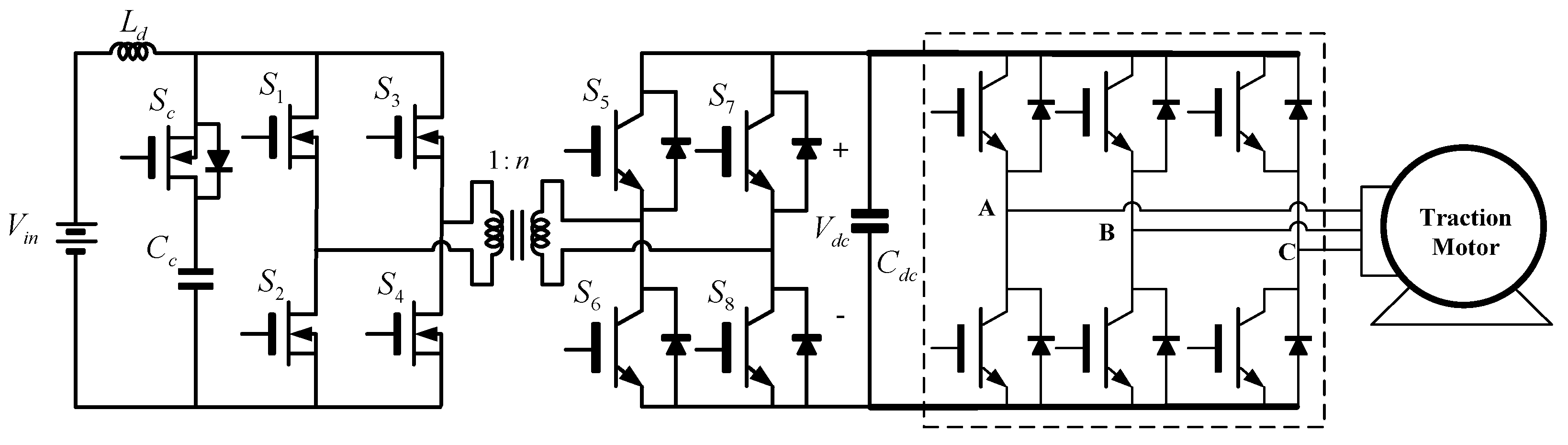
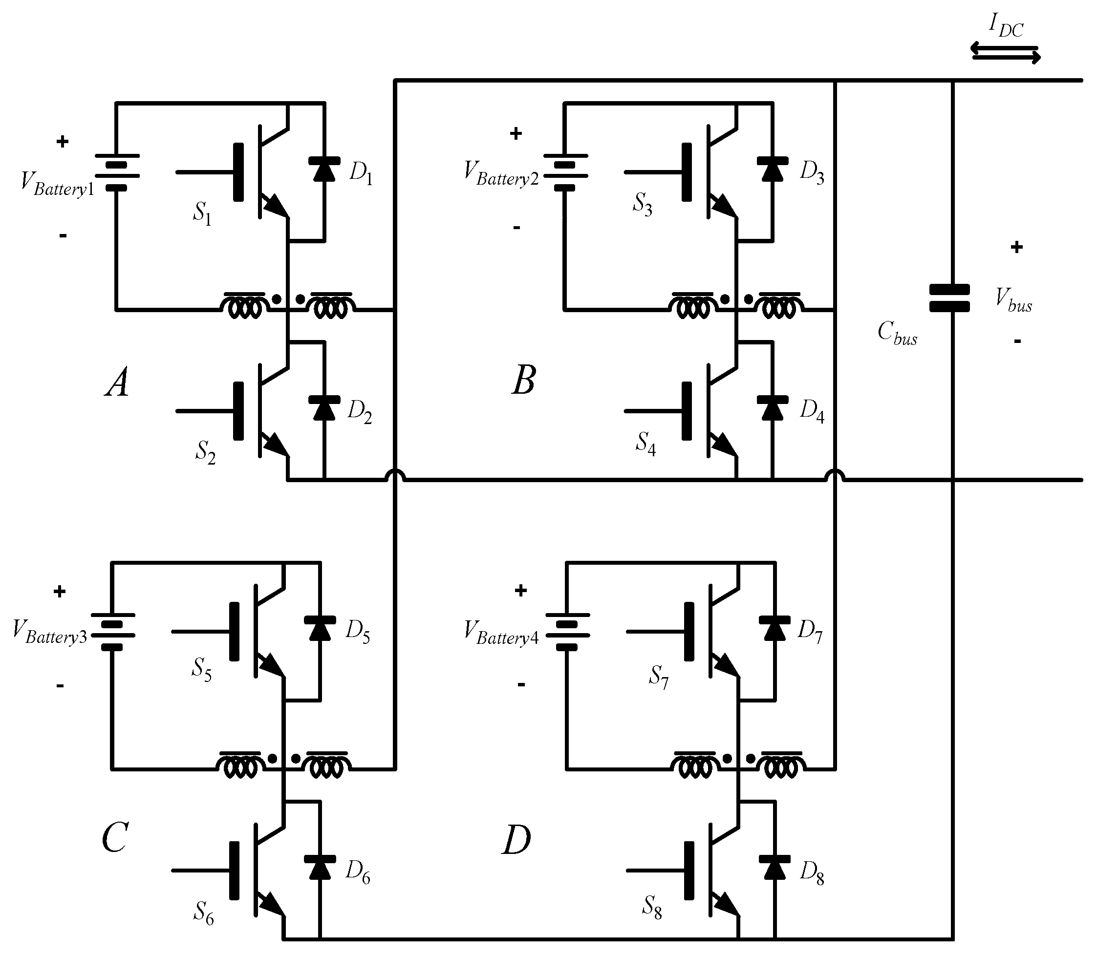
2.8. Composite Converter Approaches
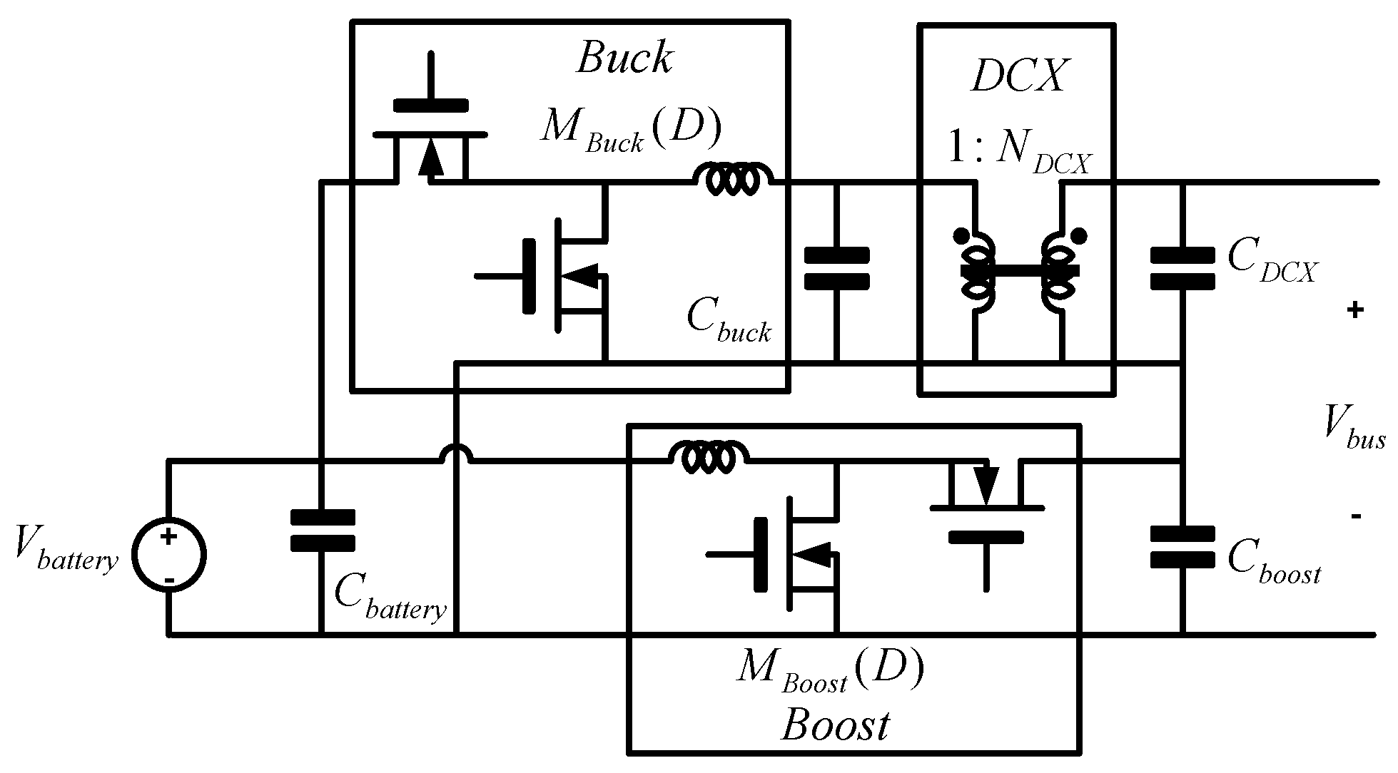
This approach is new towards efficiency improvements at wide load ranges, i.e., medium-to-light load conditions, which are very critical for electric vehicle powertrain. Previously discussed topologies have incremental efficiency improvements, whereas, in this topology, several smaller different converter modules are combined to process the total system power.
Further, depending on the converter, operating conditions shut down or pass-through modes are used to reduce the ac loss mechanism [
35]. Average loss reduces approximately by a factor of 4, and the capacitor size reduces around by a factor of 2. The electric vehicle system is thermally limited; therefore, large heat sink requirements are also taken care of in this topology. This reveals according to the converter performance metric, which also states that if Q gets doubled, then power output gets doubled in a thermally limited system while system cooling will get halved. It directly impacts the vehicle efficiency in terms of miles per gallons equivalent (MPGe) and improves the power density and reduces the size and the cost of the thermal management system. Chen et al. [
36] proposed a 30 kW boost composite converter with a peak efficiency of 98.5%, which is called a composite converter topology (D). Other variants are also proposed, such as boost composite converter (A), composite boost converter (B), and composite converter topology (C), out of which composite converter (D) is most suitable for electric vehicle powertrain. Composite converter D eliminates the drawbacks of the variants as mentioned above by utilizing a boost module, a buck module, and the dual active bridge (DAB) module or DCX module. Power from the source is distributed in a manner that fraction of power from the source is processed by the buck converter in cascades with the DCX module, and the rest of the power is processed by the boost converter module. It improves the device voltage stresses as part of the power is partially processed by two different sections of the converter; therefore, two separate power flow paths came into the picture, i.e., indirect power flow path and direct power flow path. DCX module is introduced to process the indirect power whose turn ratios are adjusted to achieve the desired output voltage, whereas input voltage is controlled via buck converters. DAB acts as a DC transformer that incorporates soft-switching techniques to improve the converter’s overall efficiency at the medium-to-light weight. The authors in [
35] have concluded the benefits and created a room for researchers to look into the advances for this topology by comparing with most appropriate converter topologies, i.e., boost, SAZZ, coupled inductors, three-level, and composite converter D. In
Table 1, power rating, capacitor ratings, and Q factor for standard driving cycles [
37] and converter size comparisons are tabulated. The composite converter D, operating modes, and its efficiency compared with other topologies mentioned in
Table 1 are shown in
Figure 18.
In a further section, there is a subject which is very tempting and valuable, i.e., condition monitoring of the power electronic converter in electric vehicles. Besides efficiency, the parameters, namely device reliability, safe operation, maximum life, cost, and thermal issues due to the presence of high voltages and high circulation currents within the converter, needs further investigation to meet an optimal solution for EVs.
3. Future Aspects of EV Technology
Given the future aspects of electric vehicular technology, there are various domains, so discussing them in detail would overwhelm the purpose of the reading, and the additional references would be countless. Therefore, from a specific technological point of view, the goals of different technologies associated with electric vehicle advancement have been discussed here. Further, readers will have an overall intuitive idea about the role of power electronics together with other domains as per the recent updates in the technologies as follows:
Semiconductor technology
Power electronics and drive train technology
Motor technology
Battery and its management technology
Control engineering technology
Vehicle to grid (V2G) technology
Home to grid (H2G) technology
Wireless energy power transfer technology (WPT)
Grid integration of EVs
Therefore, all these broad research areas have a different perspective on electrical engineering behind electric vehicles, as semiconductor devices are the heart of electric vehicles’ power electronic systems. Further, it has a significant impact on the development of power electronics technology for an electric vehicle regarding reliability, cost, efficiency, and dynamics. Besides, various motor control and battery technologies need to be developed concerning the electric drive system, where batteries are critical and highly flammable at high temperatures. Various battery management systems (BMS) are in development for Li-ion cells as they are prone to hazard at high temperatures. Further, other alternatives are needed to be explored because of the batteries’ electrochemical process, which may be reversed by using nanomaterials so that decomposing the battery after the end of the life cycle can be avoided. Because of motor technology, there are various motors available in the field for electric drive, i.e., brushless DC motors (BLDCs), switched reluctance motors (SRMs), permanent magnet synchronous motors (PMSMs), which are very popular among EVs. Several issues remained to be solved, such as cost, size, weight, control methods, fast dynamic response, and high efficiency.
Further, control engineering plays a vital role in sustaining all the systems within the vehicle in a highly stable state as the power electronic system requires control systems to maintain the vehicle’s excellent dynamic performance in the presence of any disturbances. Therefore, challenges raised in this domain are very critical subject to the dynamical conditions of the vehicle. One has to control the battery system’s temperature and decide when to operate in battery mode or internal combustion engine mode, control of bidirectional energy flow between the battery pack and the drivetrain, and control power electronic converters the proper operation of the drivetrain, etc. Potential mathematical modeling of power electronic converters is necessary because of controlling the issues mentioned above, i.e., small-signal modeling, steady-state modeling, controller design modeling, circuit averaging methods. Also, magnetics design modeling, filter designs, and advanced analog control techniques for power converters like voltage mode control (VMC), current programmed control/current mode control (CMC), Peak current mode control (PCMC), average current mode control (ACMC) may be emphasized. One may intermix the control methods for further technology advancement using digital control methods, neural networks, genetic algorithms, fuzzy logic, and other optimization methods for major controlling issues for their implementation.
Vehicular technology because of V2G, H2G, and WPT is again a new emerging domain for revising power systems. These technologies help our power system maintain power system stability since the power system’s load curve throughout the day has to be constant. If the right time charging incentives are considered adequate but provided, customers have to understand electric vehicles’ use as per the grid load dispatch laws. Further, Grid integration of these vehicles needs additional efforts for connecting EVs to the power grid as power electronic systems are prone to harmonic injection into the grid. This can lead to power quality issues where the phase-locked loop (PLLs) system’s significant role plays a vital role in grid-tied converters. In addition to it, adequate care needs to be taken according to their life cycles as high circulation currents and over-voltages are subject to matter, which is required to be addressed. In the next section, condition monitoring aspects of these converters are highlighted, which is necessary to mitigate the life cycle mentioned above concerns of power electronic converters.
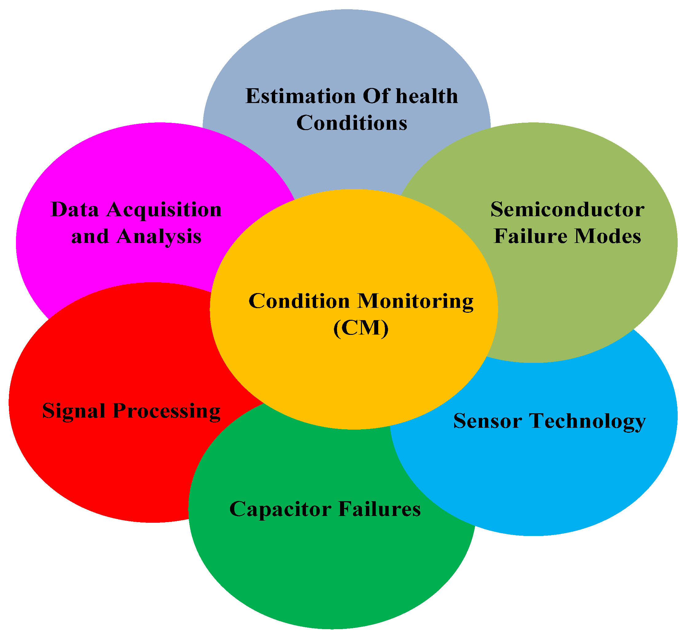
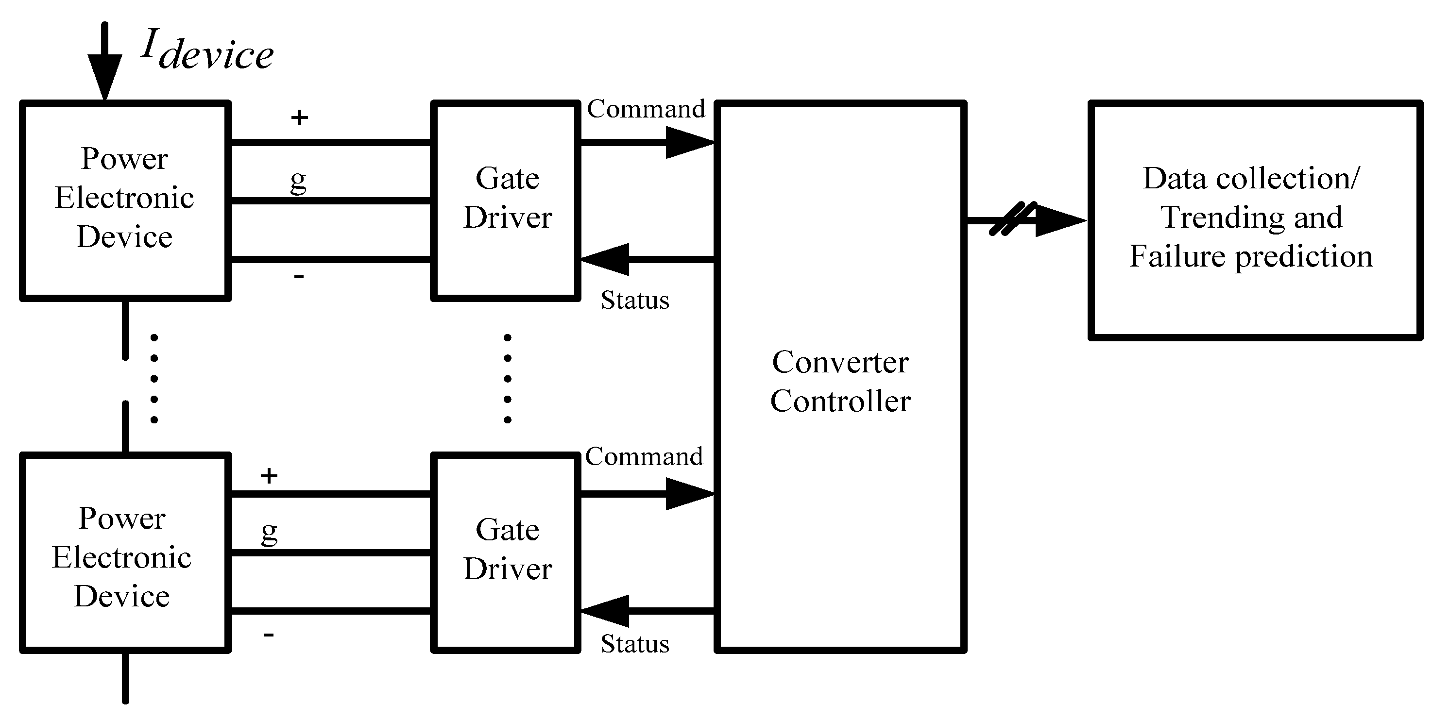
4. Condition Monitoring of Power Electronic Systems
Conditioning monitoring (CM) of power electronic devices is a significant area of research since device reliability, good health throughout the varying operating conditions, and life cycle of the device at a cheaper cost is critical for the industry implementation of power electronic converters. Further, capacitors are another source of failure in power electronic converters, which need to be addressed, as the converter’s good health is entirely dependent on the circuit components throughout its lifetime. This section of the article will cover up various challenges faced by industry manufacturers related to power electronic systems’ reliability. Different methods and algorithms are adopted to diagnose the issues related to life and condition monitoring of various power electronics components. However, the dc-link capacitor used in the electric vehicle’s powertrain architecture is no more different from the capacitors of various topologies associated with EVs. Yet, Yang et al. [
38] have already reviewed semiconductor device failures in the past. This article highlights the work considered and key findings to make readers aware of past challenges. Further, Wang et al. [
39] examined the conditioning monitoring aspects of capacitors utilized in the power electronic converters. CM is in the embryonic stage; however, progress is made to understand the drifts in the healthy condition of the power electronic systems to take appropriate action in the components’ real-time state. CM is a technique or a process of monitoring the operating characteristic of a physical system so that the change of the monitored part can be used to schedule maintenance before severe deterioration or breakdown occurs [
40]. The knowledge domain embraced by CM is shown in
Figure 19.
Fault detection is mainly divided into three categories are as follows:
- (1)
Diagnosis: To identify the root cause of the given fault that occurred in the system.
- (2)
Prognosis: To predict the health of the component at some point of failure w.r.t the element’s initial health level.
- (3)
CM: To measure the real-time condition of the component if its health drifts away from the healthy state and preventive action can be taken.
Prediction of failures is necessary as catastrophic accidents result in a high penalty related to cost. Further, awareness about the power devices’ failure modes and associated sensor and signal processing techniques helps develop an efficient CM system for power electronics systems. The conditioning monitoring concept is divided into two categories, i.e., degradation failures and measured physical states. Degradation failures require the knowledge of failure mechanisms related to the device or overall system, whereas measured physical states require how to monitor performance degradation with practical techniques.
Besides the concepts mentioned above, the reliability of power devices and their aging and failure mechanisms bring in the new domain of reliability modeling approaches directly related to device structural, thermal, and mechanical aspects. Stresses produced on power electronics systems are due to electrical loading, mechanical vibration, and environmental conditions. Held et al. [
41] show that the power cycles are a critical factor for the traction system’s reliability as they affect the lifetime of power device packaging. Failure In Time (FIT) is another quantity coined for detection of failures per device hour, according to which 1FIT = 1 × 10
9 failures per device hour. If we discuss about IGBTs-FITs has reduced from 1000 FITs (year 1995) to 20 FITs (year 2000) [
41]. Reliability requirements 1 of power devices depend on the failure distribution, i.e., soldering failures in device modules (13–14%) [
41], failures due to power devices (21–38%) [
42], Capacitors failures (30%), PCB failures (26%) and other failures (i.e., connectors) (10%). The two most common types of failure mechanisms are noticed, which are titled as follows: chip-related failures and packaging related failures, whereas chip-related failure mechanisms. The same are subdivided as: electrical overstresses (EOS); electrostatic discharge (ESD); latch-up and triggering of stray fields; charge effects-ionic contamination of hot carrier injection; electro-migration, contact, and stress-induced migration; thermal activation; external radiation-mobile ions and radiation; other mechanisms for MOS gated devices [
43,
44,
45]. EOS and ESD are major chip-related failure mechanisms since they affect over-voltages, overcurrent conditions, and gate puncture. Further, packaging related failure mechanisms are subdivided as: comparison of packaging types; bond wire lift-off; solder fatigue, electrical stress effects [
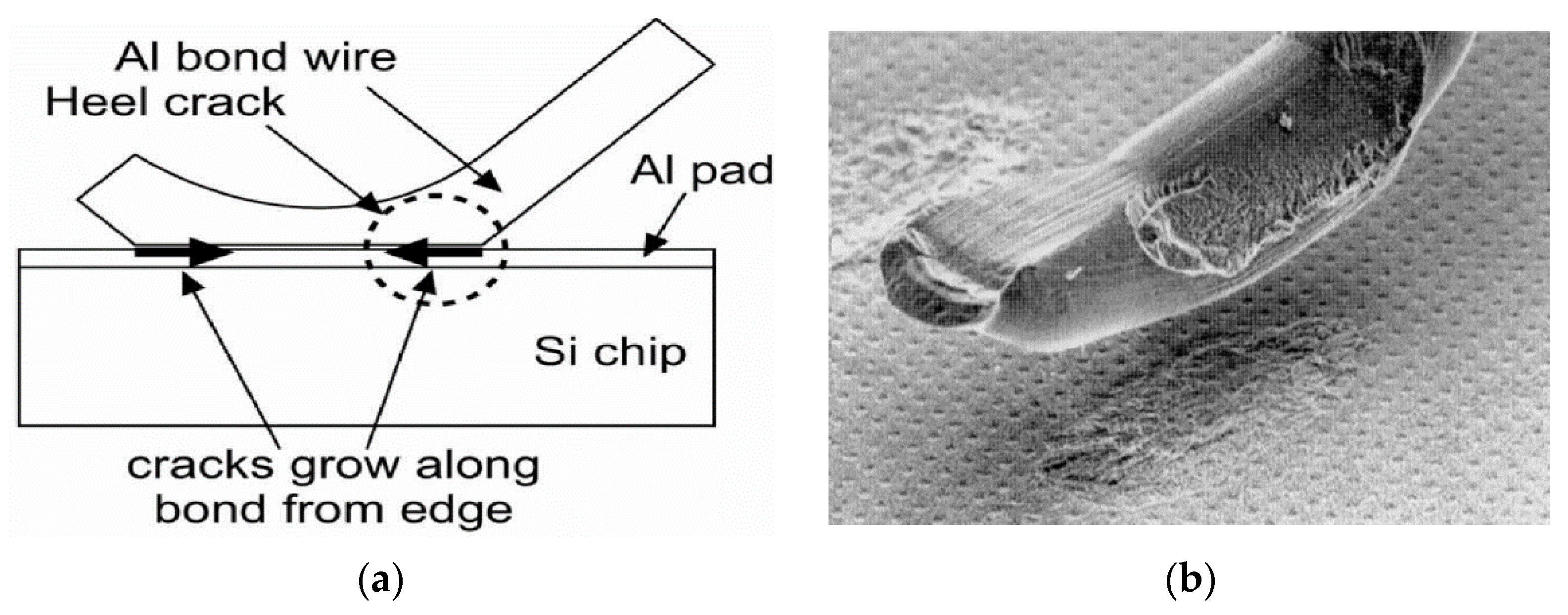
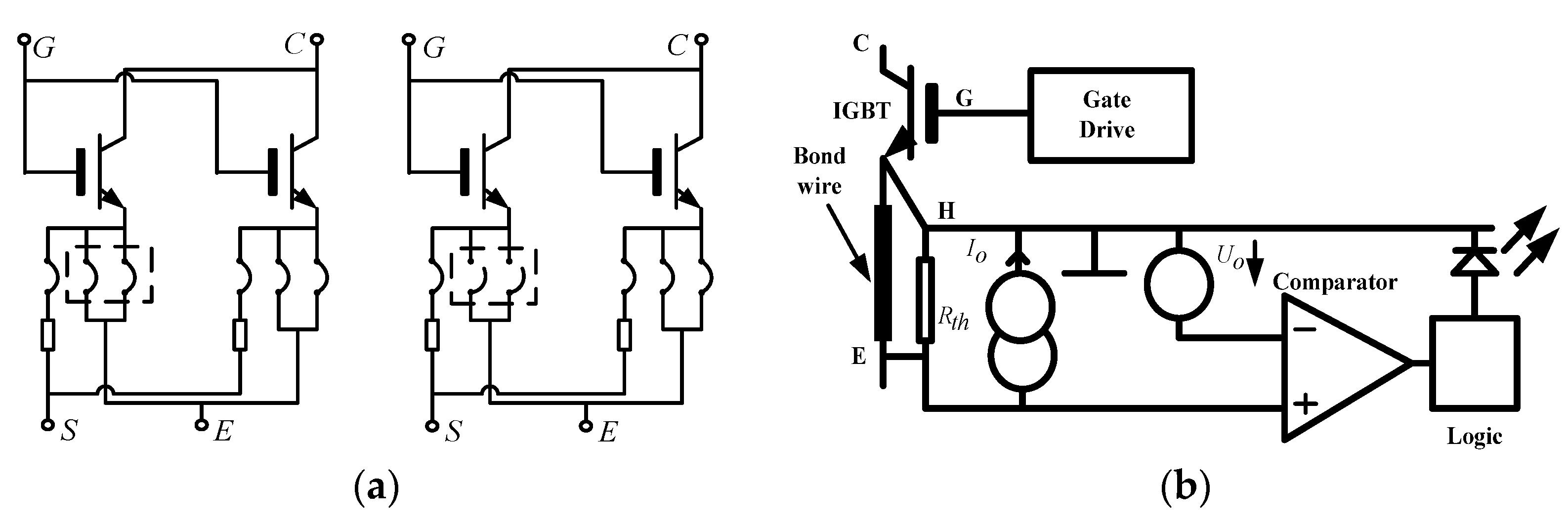
46]. Bond wire lift-off is regarded as the principal failure mechanism in the power electronics module that is demonstrated in
Figure 20 [
38]. Due to dissimilar metal contacts, i.e., Al and Si, there is a mismatch in the coefficient of thermal expansion (CTE), which increases the probability of crack growth at the material interface.
Various reliability models are proposed on the knowledge of failure mechanisms for the implementation of CM, failure analysis, and lifetime prediction. Reliability modeling follows two steps for modeling, i.e., (1) Electro-thermal modeling and (2) Thermal-mechanical modeling. A comprehensive review of these models has been done in reference [
47]. Methods are categorized in
Table 2.
4.1. Challenging Issues Behind Reliability Modeling Power Electronics Converters
How to identify crack initiation and its propagation;
How to set loop-up table methods for FEM analysis;
Creep dependent solder fatigue issues;
How to develop simple methods for predicting packaging lifetime;
How to indicate Non-linearity in packaging;
How to develop and implement advanced methods for bond wire lift-off and solder cracking.
Reliability models are tools to predict failures but cannot prevent them. However, CM can serve as a scheme for deciding which type of maintenance is required based on the reliability models to avoid failures and increase system components’ lifetime as a well-complete system. Due to the power devices’ high power density, it is difficult to measure the type of stress accurately. Instead of capturing the fault signatures in the external environment, directly related to the converter-control operation, its protection is more effective as most of the failure mechanisms are developed by temperature excursions and various converter losses.
4.2. Implementation of CM
CM may be implemented in three ways, which involves all the aspects mentioned above are as follows:
- (1)
Prevention of the changes that occurred in the operational characteristics of the device or at the converter level. Some of the parameters difficult to measure, i.e., ON-state voltage or resistance VCE,sat or RON, threshold voltage VGE,th, and internal thermal resistance Rth.
- (2)
Prevention of physical degradation of devices using dedicated embedded sensors for direct measurement of degradation.
- (3)
Under varying load and ambient conditions, Model-based CM is used where a stimulus is applied externally to detect measured response to that predicted by a healthy model.
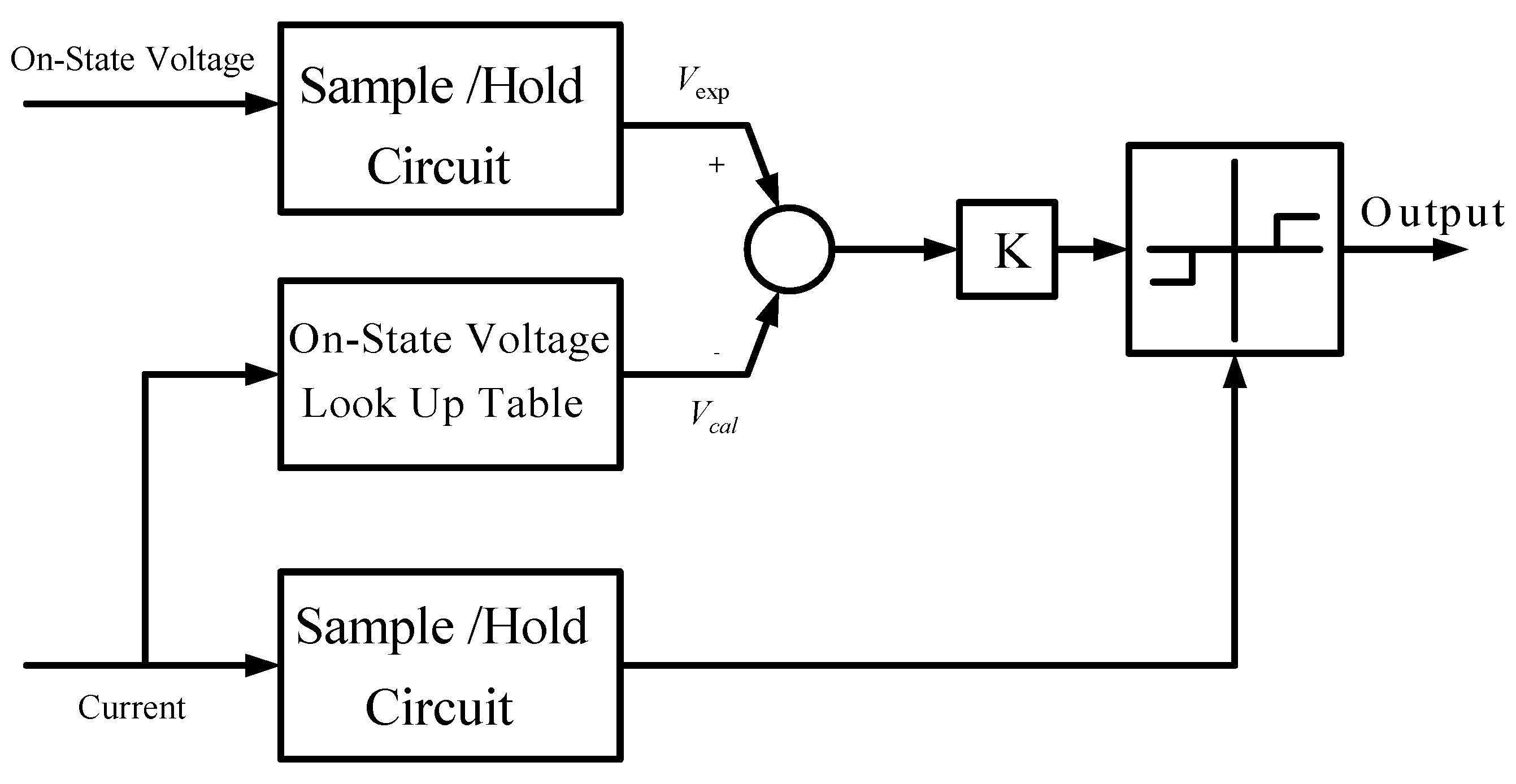
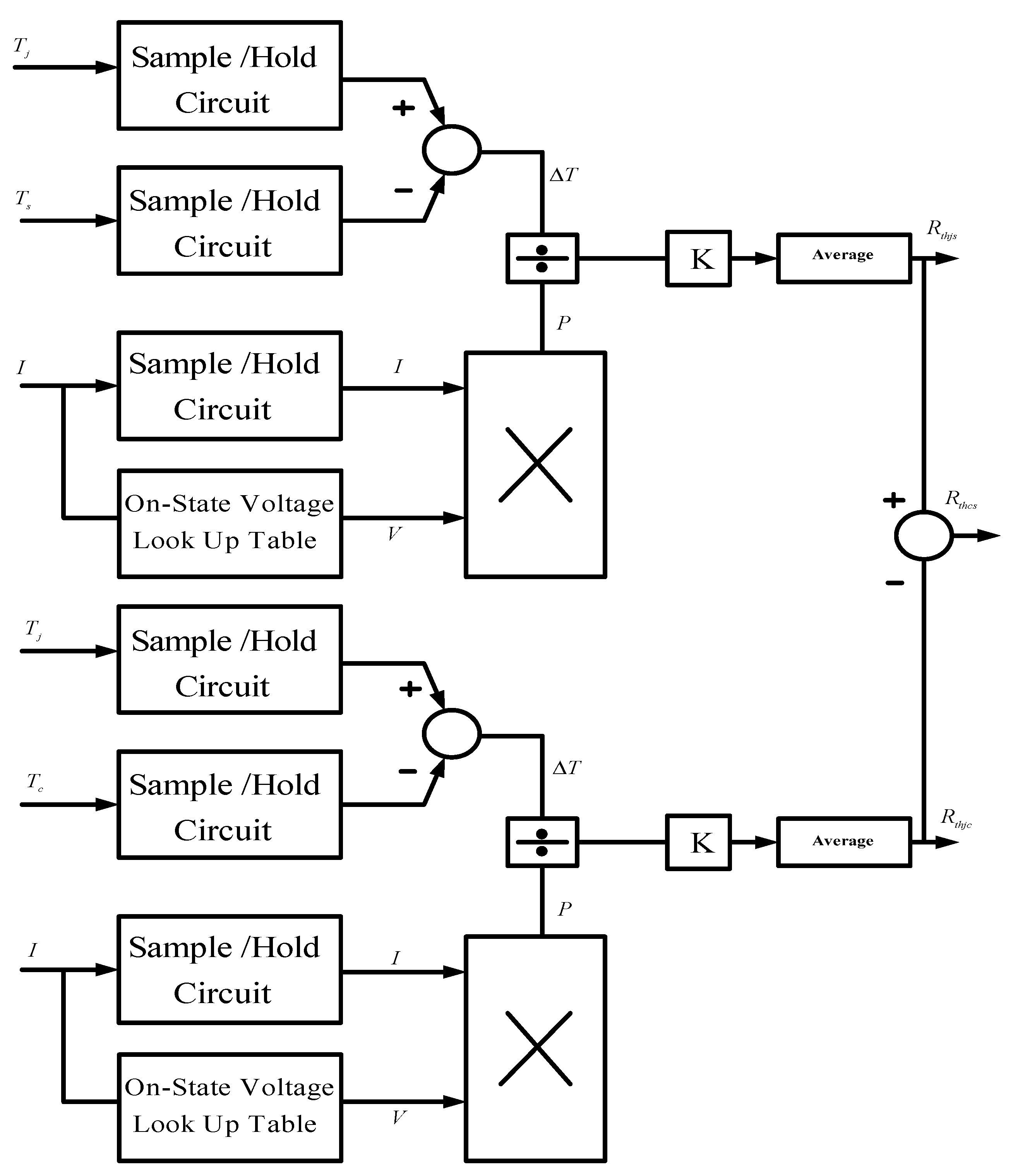
Further, CM may be based on (1) ON-state voltage for bond wire lift-off [
55] (
Figure 21), (2) thermal resistance and temperature-based [
55] (
Figure 22), (3) switch time-based for the power device and its gate driver [
56] (
Figure 23), (4) gate-signal based for gate degradation [
57] (
Figure 24),(5) sensor-based for bond wire lift-off [
58,
59] (
Figure 25), (6) system identification [
60]-based (
Figure 26).
A brief summary of all these CM schemes is a follows: (1) To trace any change in V
CE,sat or R
ON, intelligent power modules (IPMs) are used where lookup tables are updated according to the various power cycles. (2) Solder fatigue causes variation in thermal resistance, and its characteristics deviate over time; embedded sensors in the modules mounted on heat sinks detect the changes to measure the temperature over an extended period. (3) IMPs are prone to switch time failures such as partial failure of a multichip device, high junction temperature, and gate driver circuit degradation, for which a monitoring technique is developed by Coquery et al. in [
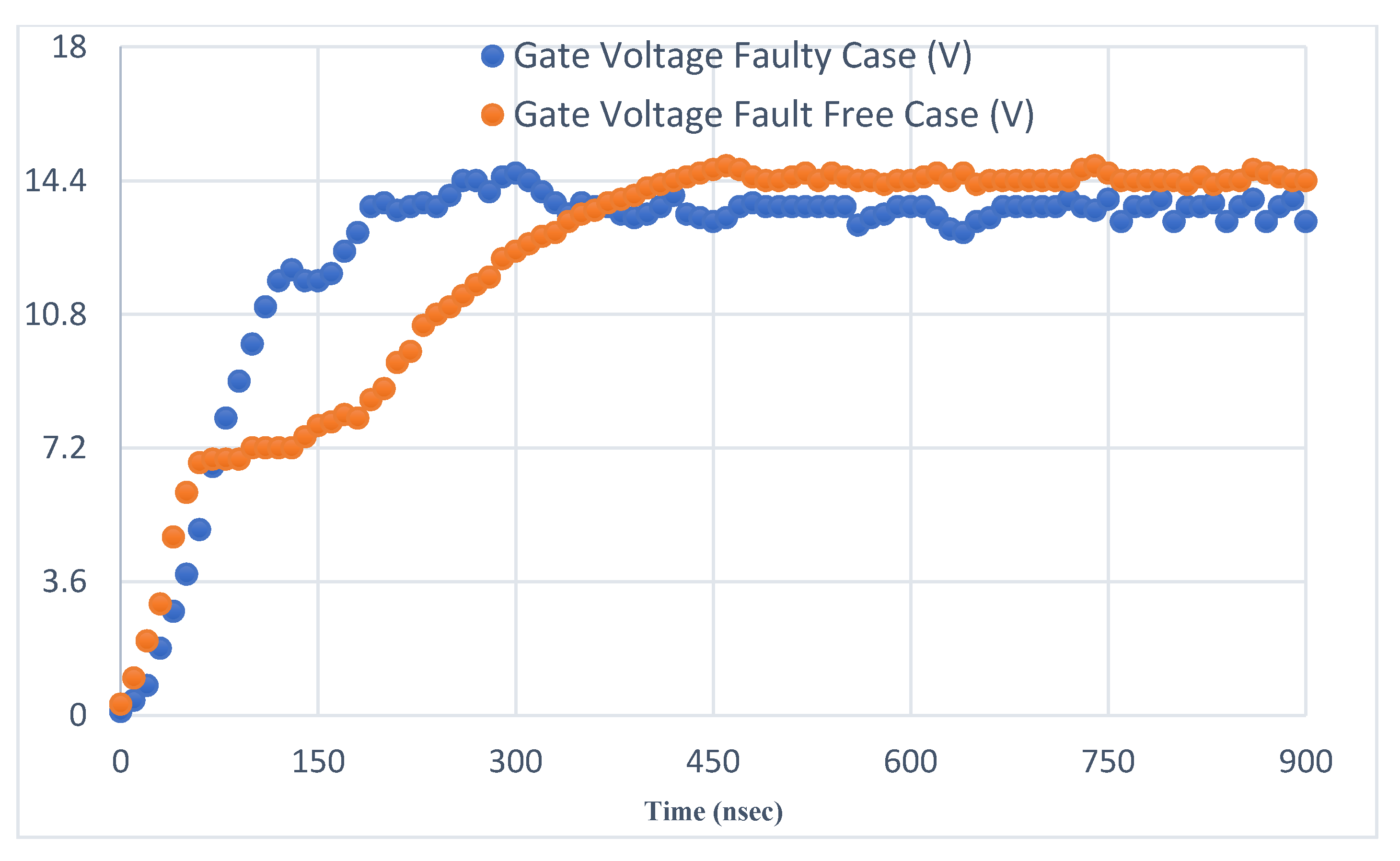
61]. Where during normal operation, thousands of switching operations are recorded every second, and a regression measurement technique is used to detect every possible failure. (4) Short circuit fault in an IGBT was proposed by Rodriguez et al. [
57] and based on gate voltage waveform, which is specified during turn ON of the device since device degradation occurs due to the gate charge distribution (
Figure 24). However, it was not clear to observe the difference between the gate signals of the device in a non-fault and the fault conditions. The investigation suggests that a certain threshold setting may be used to identify natural ageing of the device owing to the existence of the short circuit faults. The ageing effects are, therefore, must require additional efforts, (5) Lehmann et al. [
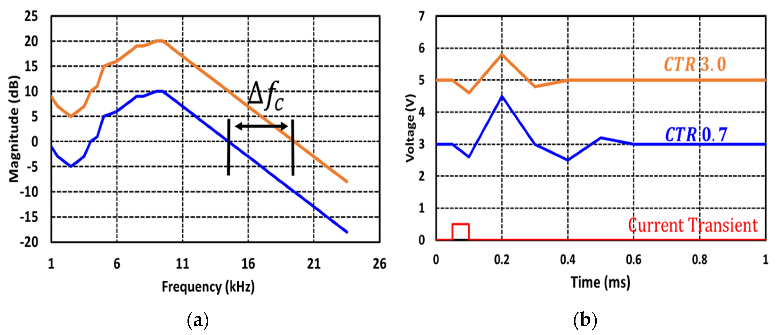
58] proposed a sensor-based scheme to detect bond wire lift-off in an IPM where an instrumentation circuit is inserted between S and E. (6) Optical isolator degradation is another crucial device in the feedback path for the voltage regulation of converter to monitor its degradation current transfer ratio (CTR) is used. Further, for the optical isolator’s health monitoring, we need to observe the change in the crossover frequency
. If CTR falls below a critical threshold value converter to regulate the output voltage, a test step is used for output voltage transients with a load current spike of 5 A [
60]. Another conditioning monitoring domain that requires further investigation is the conditioning monitoring of capacitors used in power electronic converters. The article’s topologies consist of this type of passive component for its energy storing and filtering capabilities. DC link capacitor is one of the critical elements of electric vehicle powertrain architecture; therefore, its size, cost, and health influence the power converter’s overall power density and reliability.
In general, there are three types of capacitors available, i.e., electrolytic capacitors (E-caps), metalized polypropylene film capacitors (MPPF), and multilayer ceramic capacitors [
62]. The malfunctioning of the capacitors in the system generally depends on the end of life, which decides the time to failure of the capacitor or multiple capacitors. In power electronics applications, we will find situations where capacitors banks are used to withstand higher voltage stresses more as compared to the single capacitor. As a result life of the capacitor bank will be more for a single capacitor.
As the time to failure of these banks may vary if one of the capacitors reaches its end of life, therefore, for reliable operation, we need to replace the entire bank [
63]. H Wang et al. [
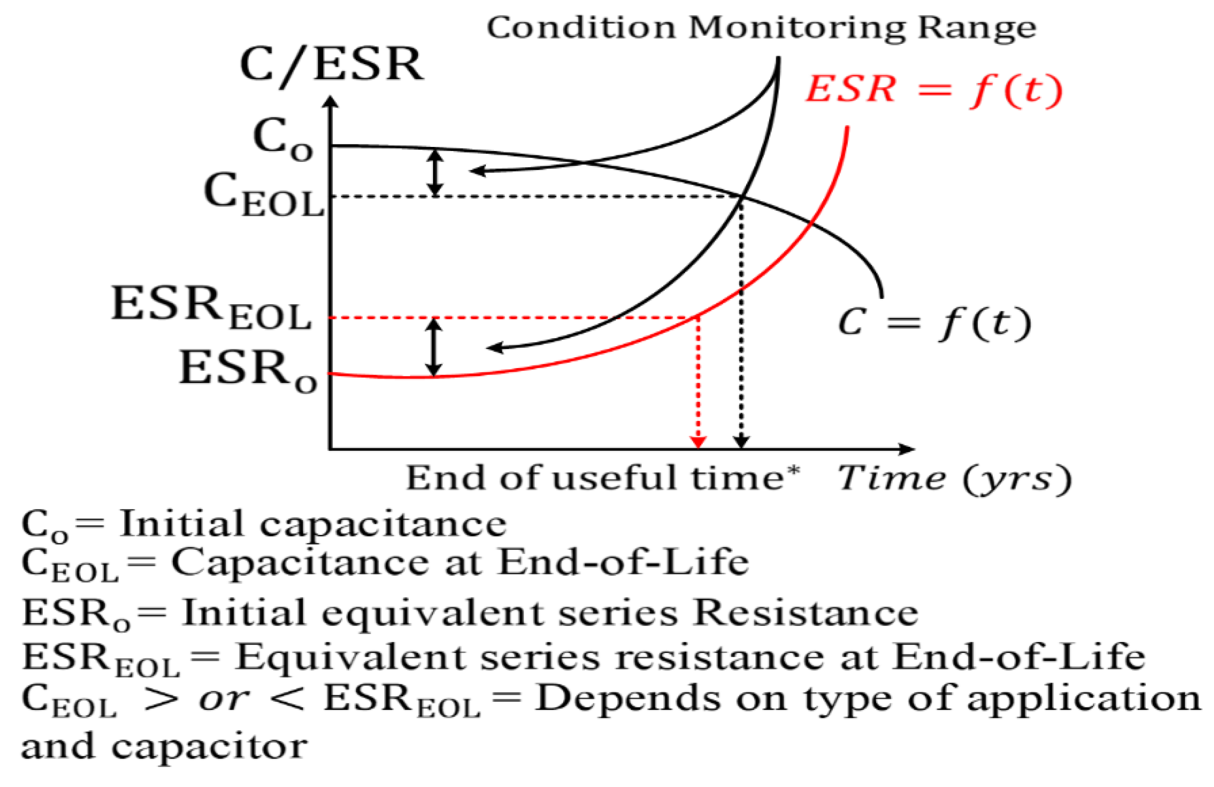
39], as showed in
Figure 27 that the degradation of capacitors or capacitor banks is dependent on capacitance C and equivalent series resistance (ESR). The end of life (EOF) or threshold criterion is essential in the capacitor’s health monitoring that is directly linked to C and ESR of the capacitor. In general, for E-caps, EOF is about 20% capacitance reduction or double the ESR, whereas for film capacitors 2–5% capacitance reduction. EOF criteria have two aspects [
70], i.e., (1) if specified EOF criteria are met, and then the capacitor degradation rate (dC/dt, dESR/dt) becomes faster (2) if capacitance drops or the ESR increases to a specified level then the power electronics circuits may malfunction. As understood by the aspect one, the determination of EOF is an important consideration in order to maintain the health of the capacitors. The failures of a capacitor can be predicted by comparing the estimated capacitance (
) with the EOF. Further, a detailed capacitance or ESR degradation curve is not required in order to know the deterioration level of a capacitor, the prediction can be possible by only observing the difference between
and EOF. However, the remaining useful lifetime (RUL) estimation requires the knowledge of ESR degradation curves at varying operating conditions with the help of accelerated degradation testing data, the RUL may be estimated accurately. The capacitor condition monitoring methodology are classified as (1) Online approaches and (2) Offline approaches. The performance indicators which are needed to be considered for employing the conditioning monitoring techniques for capacitors, i.e., ESR, capacitance (
), ripple voltage, volume and temperature (
). Accordingly, the prevalent methodologies are, therefore, categorized as follows:
- (1)
Capacitor ripple current sensor-based methods [
64,
65,
66,
67]
- (2)
Circuit model-based methods [
68]
- (3)
Data and advanced algorithm-based methods [
69]
On the other hand, several future research opportunities [
39,
69] for condition monitoring of capacitors includes following important points:
- (1)
Software-based methods—reduced hardware computational complexity along with improved reliability.
- (2)
Improved current sensing technology may help to reduce the overall cost.
- (3)
Applications requiring high reliability must incorporate and implement the protection, and other ancillary functions along with the conditioning monitoring of capacitors.
5. Conclusions
In this article, the importance of and need for automated electrical vehicles have been emphasized by identifying potential topics. The important issues that need a potential expansion of existing knowledge have been the survey’s target topics. The details, summary, and critical analysis of the existing bidirectional converters that are suitable for use in automated electric vehicles have been reported. The service performance of the various components in the vehicles is important to reach the electric vehicle’s theoretical designed life. Thus, condition monitoring aspects, methodologies, reliability challenges of various electronic components used in electric vehicles have been reported. Notably, the future aspects and reliability challenges concerning electric vehicles have also been addressed. Part 2 of this survey focuses on the printed antennas and sensor aspects for automated radar applications in autonomous electric vehicles.


 ,
, 


