1. Introduction
A coupled inductor has more than one winding wound on the magnetic core. It is typically used for energy storage [
1,
2] in many power electronic networks such as electric energy storage systems, electric vehicles, or photovoltaic systems [
3,
4]. The abovementioned systems require the use of various types of converters. Such systems are characterized by energy efficiency and high voltage amplification [
5].
In the mentioned papers, coupled inductors are used to achieve a higher value of the voltage amplification factor of a high voltage converter [
3] in order to reduce the ripple current in a multiphase buck converter with fast response time and to reduce steady-state power losses [
6,
7]. In addition, they are used to achieve high step-up voltage conversion of a zeta converter operating in the photovoltaic system or a high step-up DC–DC converter dedicated to operating in renewable energy applications [
4,
8]. In this case, a proposed, new topology of a high step-up DC–DC converter made use of a coupled inductor to obtain high step-up voltage, and the problem with the energy stored in the leakage inductance was solved by recycled leakage inductance using of a passive clamp circuit [
4]. On the other hand, the coupled inductor in the paper [
9,
10] was used to achieve a significantly high voltage gain of a high step-up converter without necessarily using a high value of the duty cycle. This type of a solution is dedicated to fuel cell energy source applications [
10,
11,
12]. In turn, in [
11], a DC–DC boost converter topology with a three-winding coupled inductor for low input and high output voltage applications was proposed. This topology is dedicated especially for photovoltaic systems, fuel cell systems, high intensity discharge lamps, and electric vehicles. The coupled inductor in this topology was used to increase the voltage gain, and it enhanced the utility rate of the magnetic core and power density. It was also used to reduce the stress on the power components of the considered converter.
As noted in the papers [
12,
13], using coupled inductors allows for reducing the number of system components and minimalizing the size of the inductor. Additionally, the value of the coupling coefficient proposed by the manufacturers of the coupled inductor reaches 0.995 [
14,
15]. As a consequence, it means lower power losses and higher energy efficiency of the designed switch-mode power systems [
15,
16].
For example, Moghaddam and Van den Bossche proposed a new topology of a forward converter dedicated to lithium-based batteries in an electrical vehicle application [
3]. In the proposed solution, a forward balancing method is used that does not require a reset winding circuit in order to demagnetize the transformer’s primary winding. Additionally, a transformer with one primary and eight secondary windings is applied. To avoid non-uniform voltage distribution in the secondary windings, a hairpin winding is used. The topology presented in [
5] confirms the legitimacy of using transformers or a coupled inductor, because they allow for a reduction in the number of components and maintain high energy efficiency for the system.
The paper [
14] presents the benefits of the applied coupled inductor in the SEPIC converter. It has previously been mentioned that coupled inductors are mainly chosen because they allow for a reduction in the number of the system components, and a fewer number of turns is required while using two single inductors. Additionally, the coupled inductors reduce AC losses by leakage inductance. The paper presents, also, a comparison of the computational results of the characteristics of SEPIC converters with the coupled inductor and with two single inductors. The obtained results show that the energy efficiency of the SEPIC converter was higher by approximately a few percent when the coupled inductor was used. This efficiency usually increases when the input voltage of this converter increases.
As it is presented in the papers [
15,
17], the trend to minimize the number of components in power electronic systems has been observed. One way to minimize magnetic component is by replacing a few inductors with a coupled inductor.
The paper [
17] presents a modified step-up DC–DC Flyback converter with the active snubber for improved energy efficiency. The proposed topology includes three identical coupled inductors with the unity turns ratio. The authors of the mentioned paper take into account different operating modes and present mathematical analyses of the proposed converter. On the other hand, the paper [
15] describes a DC–DC boost converter topology for low input and high output voltage. The proposed topology is based on a three-winding coupled-inductor. This inductor operates as both flyback and forward converters and should be designed as dedicated to a flyback converter. The authors of the mentioned paper also describe how important a good design of the coupled inductor or transformer is to ensure proper operation of the proposed converter and high energy efficiency. Additionally, the paper [
15] includes a mathematical analysis of the system depending on its operation mode.
Computer programs supporting the work of engineers are commonly used for the analysis and design of electronic and power electronics converters [
18]. Such programs are used in the analysis of such converters, and they require models of all components of the considered systems [
19,
20]. In many papers (by different authors), averaged models are used for the analysis of this type of systems [
21,
22]. In the book [
23], commonly used DC–DC converter topologies are discussed. These converters include linear and nonlinear components. The models proposed in the mentioned book can be implemented in SPICE software. For example, the papers [
24,
25] present models of an inductor dedicated for the analysis of DC–DC converters, whereas the papers [
26,
27] describe averaged models of magnetic and semiconductor devices which take into account more phenomena occurring in electronics components than the averaged model of switch mode power converters proposed in the paper [
28].
The mentioned models, however, neglect such effects as nonlinearity and delays in the operation of semiconductor devices [
29,
30]. In addition, in numerous papers which concentrate on the analysis and modeling of a coupled inductor, a T-type model, is adopted. This model is the basic transformer model, which has a structure described in the paper [
6], containing three inductors with a common node. This model is used as the first version of the model [
29,
31]. It is a subcircuit with three inductors having one common mode. However, it was noted in [
31] that the model mentioned above is asymmetric in relation to the symmetrical structure of the transformer and insufficient for the analysis of such systems as a multi-phase buck DC–DC converter, because magnetizing inductance occurs only in one of the windings [
32].
On the other hand, in [
32,
33], a model of a coupled inductor was proposed based on the concept of self and mutual inductance, described by means of basic relations known from the fundamentals of electronics [
34,
35]. Moreover, the description of this model does not include the general relationship between voltages on the coupled inductor [
36]. The authors of this paper conducted investigations on thermal phenomena occurring in the core of magnetic components [
37,
38] and in the winding [
39]. The obtained results showed that many factors, such as frequency of the signal exciting a magnetic component, temperature, magnetic flux density amplitude, and skin and proximity effects significantly affect properties of magnetic components and, ultimately, the energy efficiency of power conversion systems [
39,
40]. On the other hand, another paper [
41] presents the analysis of the magnetic design and sizing of a three-winding coupled inductor. The presented mathematical analysis can be useful as an introduction to modeling a coupled inductor, because it takes into account many variables which impact the properties of the coupled inductor such as leakage inductance, the dependence of magnetic permeability on frequency, core losses, stray capacitance, proximity and skin effect. However, it is a mathematical description that could be extended with information on how to implement the proposed solutions. Additionally, the conducted analysis does not cover the thermal phenomena occurring in the considered coupled inductor, because the description of temperature increases in the inductor’s core and the winding is incorrect.
Such investigations enabled proposals of new methods of measuring power losses in magnetic components. The mentioned losses are a result of the phenomena occurring in the core and in the winding of the magnetic component [
37,
38]. It was also possible to formulate an electrothermal model of the inductor and transformer, taking into account, for example, the self-heating phenomenon in this component, the skin and proximity effects, and losses in the winding. Taking into account the fact that the current of the inductor operating in the DC–DC converter has a triangular waveform with an adjustable rise time, the skin and proximity effects using the Fourier series approximation are defined.
As it is visible from the presented literature review, there is currently a lack of a model of coupled inductors taking into account the influence of current and frequency of the properties of this device. Additionally, typically parasitic elements of the windings are omitted.
This paper proposes a model of a coupled inductor with
n windings. The proposed model takes into account the influence of frequency on parameters of each inductor winding. Additionally, it takes into account a nonlinear dependence of inductance visible from the terminals of each winding on direct current in the winding.
Section 2 proposes a model of a coupled inductor.
Section 3 and 4 present the investigated inductor and the measurement setup, respectively. The correctness of the proposed model is verified in
Section 5. A discussion of the obtained results is given in
Section 6.
2. Coupled Inductor
In order to formulate a model of an electronic component it is necessary to define sets of equations or an equivalent circuit describing the considered component. Values of the parameters of the developed model should be determined based on the measurements or the catalog data of the used ferromagnetic core.
This section presents a new model of a coupled inductor that can be used to analyze power electronics devices. This model is based on a physical model and has a form of a subcircuit for SPICE. In the proposed model, the electric and magnetic properties of the considered device are taken into account. Particularly, this model takes into account: the nonlinearity of a magnetization curve of the used ferromagnetic core, nonlinearity of inductance of each winding, magnetic couplings between these windings, power losses in the core and in the windings, and the parasitic capacitances of the windings. Particularly, the dependence of inductance of each inductor winding on its current is taken into account. The detailed description of this model is presented below.
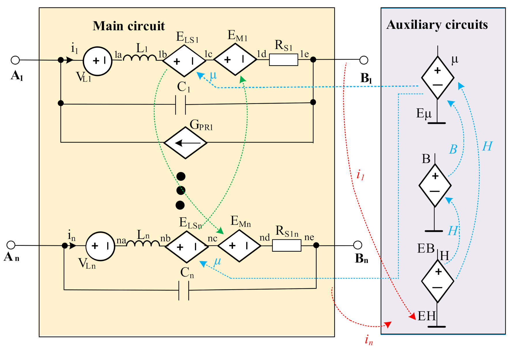
The network representation of the proposed model is shown in
Figure 1. Pairs of terminals A
i, B
i (i = 1, 2, …,
n) corresponding to the winding terminals of the modeled inductor are used for the analysis of electronic systems.
The developed model contains two blocks: main circuit and auxiliary circuits. It takes into account the influence of frequency, direct winding current, and losses in the inductor core on the characteristics of the coupled inductor. To take into account the nonlinearity of dependences presented in this section, the controlled voltage and current sources were used. The relations between individual controlled sources are marked by dotted lines with arrows.
The main circuit describes the properties of individual windings of the modeled inductor and the influence of voltage resulting from mutual magnetic couplings on this winding. It consists of
n circuits corresponding to
n identical windings. Each of them contains a parallel connection of branches containing a capacitor, C
i, and a branch where there are 4 elements connected in series: a voltage source,
VLi, of a zero value; an inductor,
Li; the controlled voltage source,
ELSi; a resistor,
RSi. The voltage source (
VLi) monitors the value of the inductor’s (
Li) current. Additionally, only one branch has the third branch that includes the controlled current sources, G
PR1, modeling power losses in the inductor core. The
Li inductor enables for the determination of a time derivative of the inductor’s current, and its inductance is arbitrarily assumed to be 10 µH. The voltage source,
ELSi, corresponds to the inductance of the
i-th inductor winding and is expressed by the equation, which is a modified version of the dependence describing inductance of an inductor containing one winding, given in [
26]. This equation has the form:
In Equation (1), the imperfect coupling between the core (magnetic flux) and the winding was additionally taken into account. In this formula,
k is the coefficient equal to 1 V s/A
2,
z is the number of turns in the
i-th winding,
SFe is the effective cross-section area of the core,
αs is the coefficient that depends on the magnetic saturation of the core,
lFe is the magnetic flux path length in the core,
V(Li) is the voltage on the linear inductor
Li, and
µ is the magnetic permeability of the inductor core expressed by the empirical dependence in the form:
where
A is a parameter of the magnetic field,
H is the magnetic force in the core, and
αH is the coefficient depending on the magnetic field.
The capacitor, C
i, represents the capacity of the winding, and the resistor,
RSi, represents the series resistance of a single-given winding for the direct current at the winding temperature equal to the reference temperature
T0. The resistance of the resistor,
RSi, is described by the formula given in the papers [
16,
42]:
where
ρ is resistivity of copper,
ld is the winding length, and
Sd is the cross-sectional area of the winding wire.
The controlled current source,
GPR1, takes into account the losses in the inductor core resulting from the magnetic field excited in the windings. The efficiency of this source is expressed by the equation
where
f is frequency of magnetic flux density,
Pv0, α are parameters that depend on the type of the material used to build the inductor core.
In the block of auxiliary circuits, the following values are determined: magnetic force
H, magnetic flux density
B in the core, mutual inductance
M, and magnetic permeability of the core
µ. The magnetic force
H is given by the classical formula [
16]:
Magnetic flux density is expressed by the empirical formula describing a magnetization curve of the following form:
where
B0 denotes a model parameter.
In order to take into account the couplings between the individual windings of the inductor, mutual inductance between the
i-th winding and the rest of the inductor windings must be determined. The mutual inductance is modeled by the controlled voltage sources,
ELMi, described by following formula:
where
ki are the coupling coefficients between the individual coils, and
V(ELSj) is the output voltage on the controlled voltage source,
ELSj.
4. Measurement Setup
In order to verify the correctness of the developed model, the influence of frequency, temperature, and direct winding current on the parameters of the coupled inductor were investigated. These parameters are discussed later in this section.
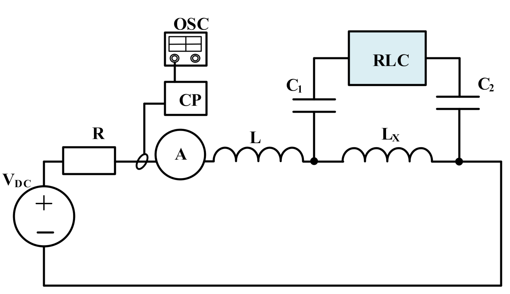
To investigate the influence of direct winding current on the inductor parameters, a measurement setup, as shown in
Figure 3, was used.
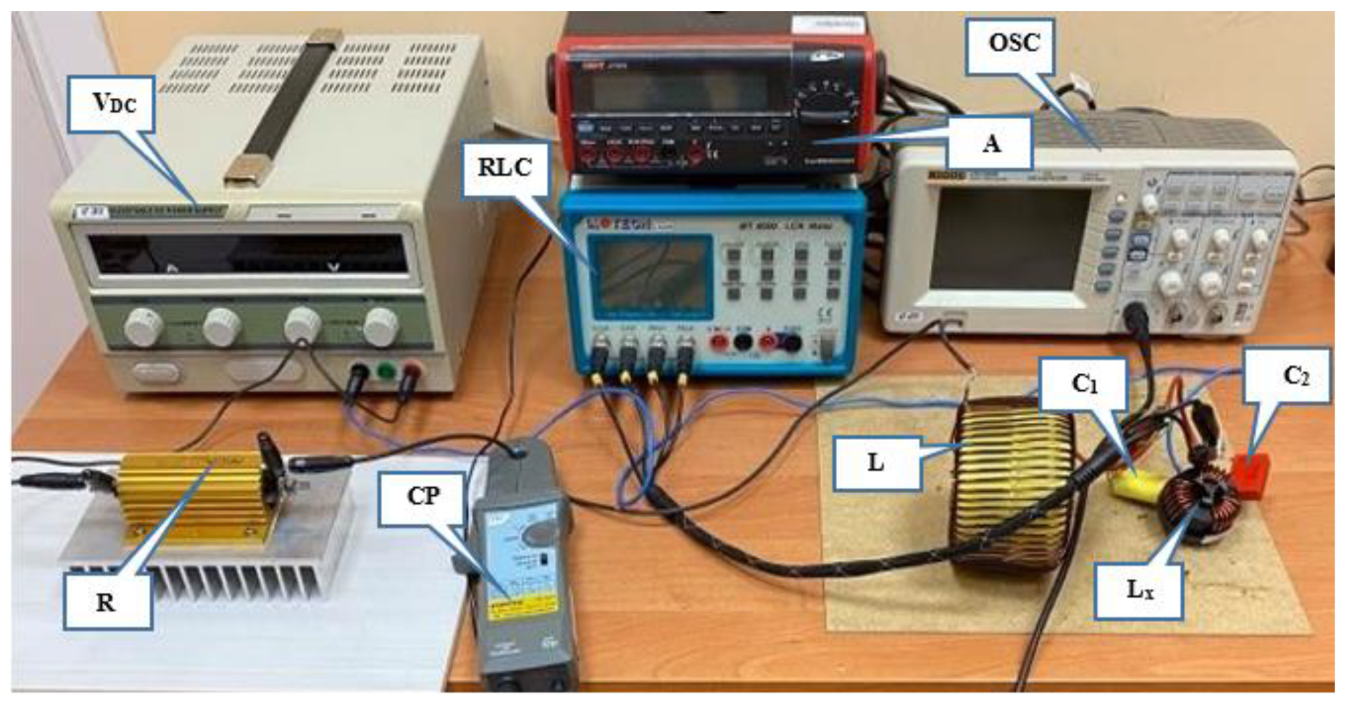
Figure 4 shows a photo of this setup. The symbols of the devices in
Figure 4 correspond to the symbols of the components in the setup presented in
Figure 3.
In the considered setup (
Figure 3), the tested element was denoted as L
x. The resistor R = 10 Ω was used to limit the value of the direct winding current of the investigated inductor from the V
DC power source. The value of this current in the range from 0 to 10 A was measured with a UNIT-T 803 multimeter (A). However, a current value above 10 A was measured using a PINTEK PA-677 (CP) current probe and recorded by a RIGOL DS 1052E (OSC) oscilloscope.
Capacitors, C
1 and C
2, with a of capacity 6.7 µF were used to protect the measuring bridge against the direct current, and L inductor of inductance 1.45 mH was used to suppress alternating current flowing through the V
DC power supply. The measurements of inductance were performed with the use of an automatic bridge of the type RLC Motech MT4090 (RLC) [
45]. The RLC bridge operated in the inductance measurement mode in a series equivalent circuit. The amplitude of the voltage generated by the RLC bridge was 1 V.
Additionally, in order to ensure a reliable measurement result, the inequality L >> L
x had to be met. The blocking inductor L consisted of 5 identical inductors connected in series. Each of them contained a powdered iron core (material type −102) with 20 turns of copper wire in enamel with a diameter of 2 mm. The geometric dimensions of the inductor: outer diameter, 10.3 cm; inner diameter, 5.6 cm; height, 6.5 cm.
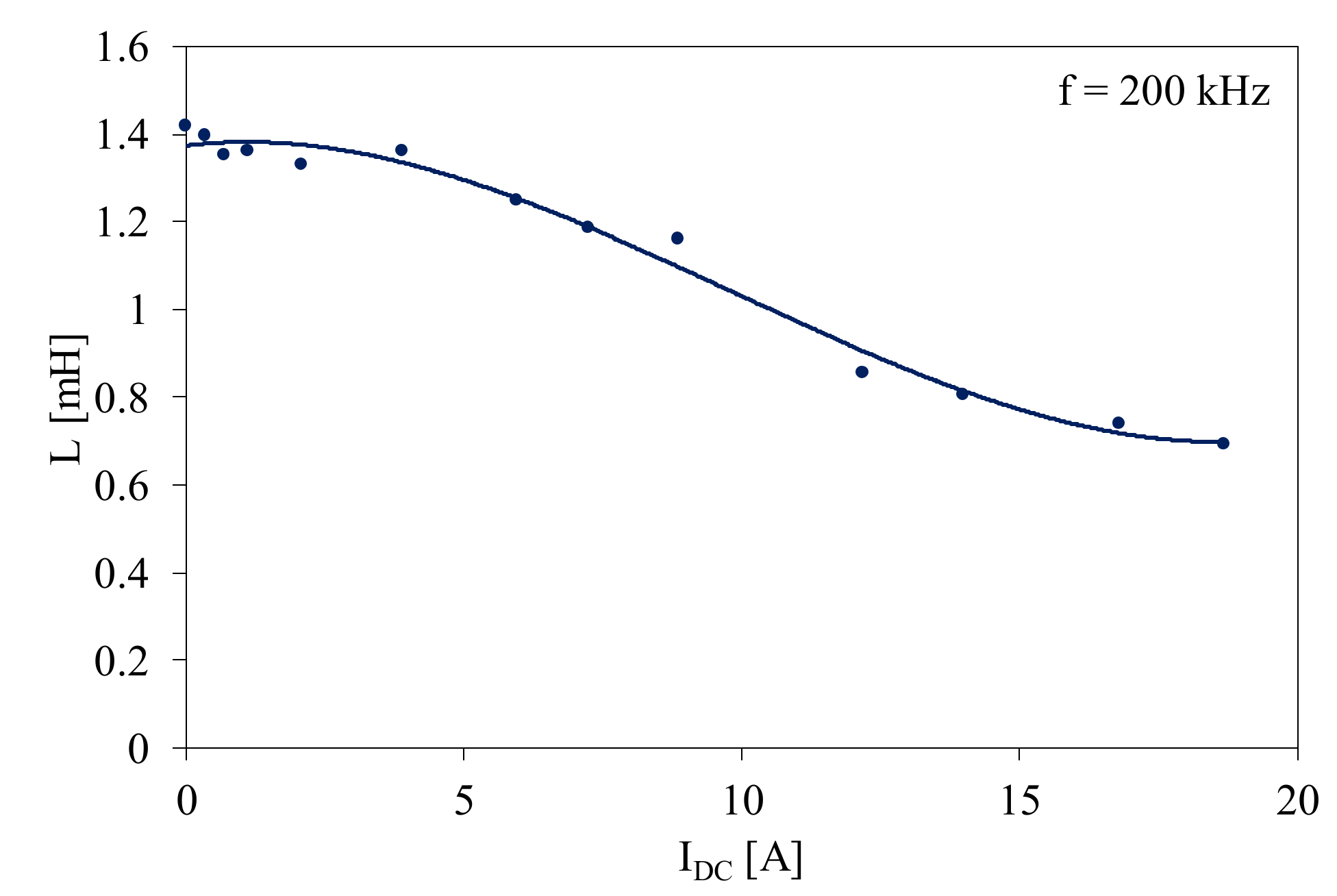
Figure 5 shows the measured dependence L(I
DC) of the blocking inductor. The measurements were performed in the setup shown in
Figure 3.
As can be seen in
Figure 5, the dependence of the blocking inductor inductance on DC current I
DC in the range from 0 to 5 A was almost constant. For I
DC > 5 A, inductance of the inductor decreased to a value of approximately 800 µH at the current I
DC of approximately 19 A.
5. Results
5.1. Validation of the Coupled Inductor Model
In order to verify the correctness of the developed model of a coupled inductor, measurements of the influence of temperature, frequency, and direct current I
DC on the parameters of the inductor were performed using the measuring setup presented in
Section 4. The obtained measurement results were compared with the calculation results obtained with the use of the model discussed in
Section 2. Except
Figure 6 for other figures presented in this section, the principle was adopted that the points denote the measurement results and the lines are the calculations results obtained using the model described in
Section 2.
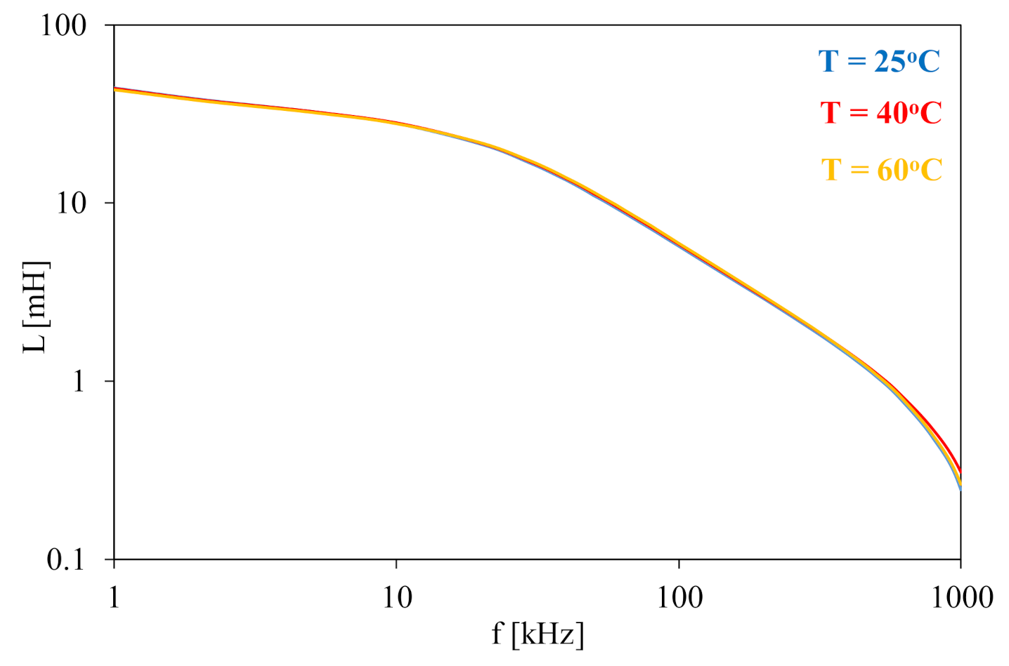
Figure 6 shows the dependence of inductance of three series-connected windings on frequency at three ambient temperatures equal to 25, 40, and 60 °C. The investigations were limited because of the allowed inductor housing temperature [
43].
The inductance of the coupled inductor with the three series-connected windings decreased with an increase in frequency over 50 times and practically did not depend on ambient temperature. Temperature changes were observed only in the frequency range above 800 kHz, and they do not exceed 6%.
Figure 7,
Figure 8,
Figure 9 and
Figure 10 present the results of computations and measurements. In all these figures, the results of the measurements are marked with dots, whereas the results of the computations are represented by lines.
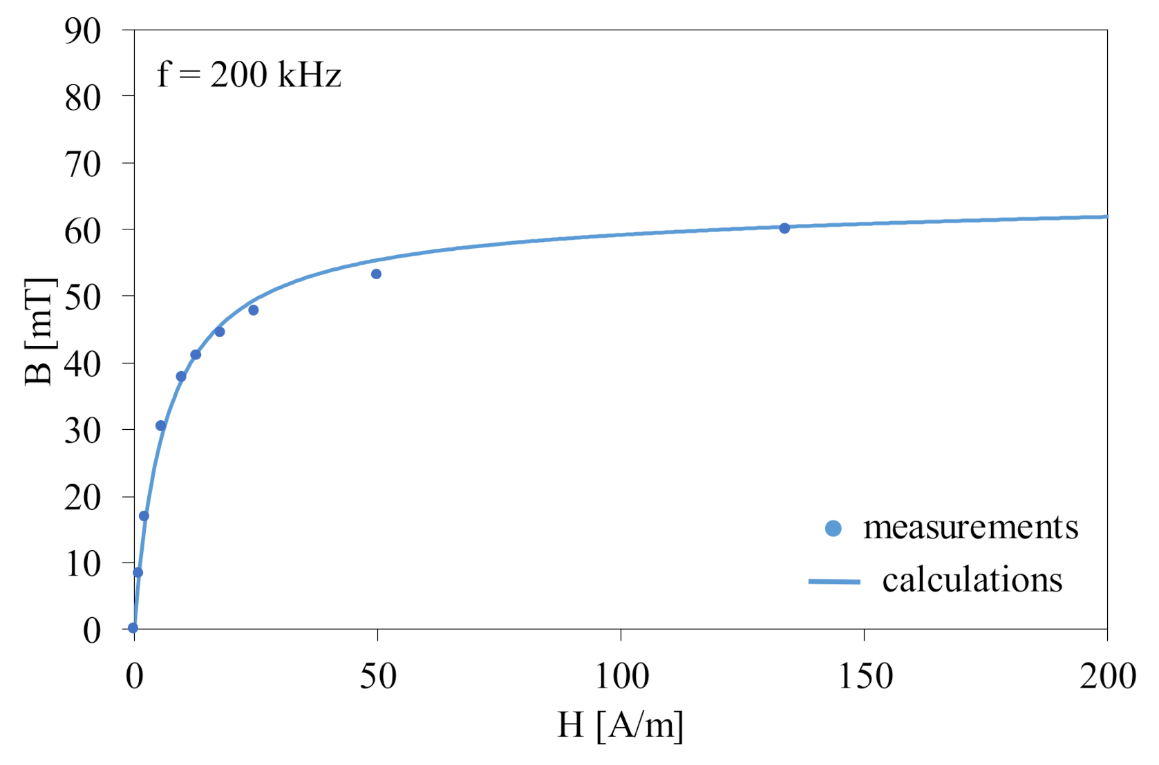
Figure 7 shows the dependence of magnetic flux density in the core on the magnetic force of the considered inductor. Values of magnetic flux density were calculated using the results of measurements L(I
DC) in the setup shown in
Figure 3 and using the dependence [
42]:
Values of the magnetic force were obtained using the dependence (6).
As can be seen, a good agreement between the results of calculations and measurements was obtained. The difference between the obtained results did not exceed 5%.
Figure 8 shows the dependence of inductance L
1 of a single winding, inductances of the series connected two windings L
12 and the series connected three windings L
123 of the considered inductor on direct current I
DC at a frequency of the exciting signal
f = 200 kHz from the RLC Bridge.
The dependences L(I
DC) presented in
Figure 8 show that the series connection of the successive windings on a common core causes an almost two-fold increase in inductance L
12 of the inductor when two coils are connected in a series, and more than a three-fold increase in inductance of the inductor in the case of a series connection of three coils. The results obtained from the calculations with the use of the proposed model are in good agreement with the measurement results. The mean square deviation of inductance between the results of measurements and calculations was equal to 1.87 µH in the range of I
DC changes from 0 to 10 A. For I
DC ≥ 10 A the mentioned deviation of inductance was equal to 0.88 µH. The measurements of inductance of the coupled inductors containing windings wound in different directions were also performed and the obtained value of this parameter was equal to about 1 nH.
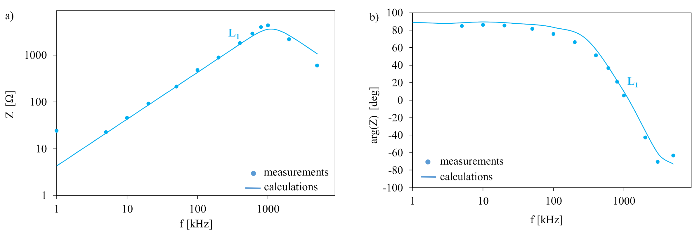
Figure 9 shows the dependence of the module and phase of impedance of a single winding, L
1, in the investigated inductor on frequency. The calculations and measurements were conducted in the setup shown in
Figure 3. The measurements were made with the value of the current I
DC equal to zero. The measurements were made using the setup presented in
Figure 3, but instead of the Motech RLC bridge, the LCR-8000G GWINTEK bridge [
46] was used.
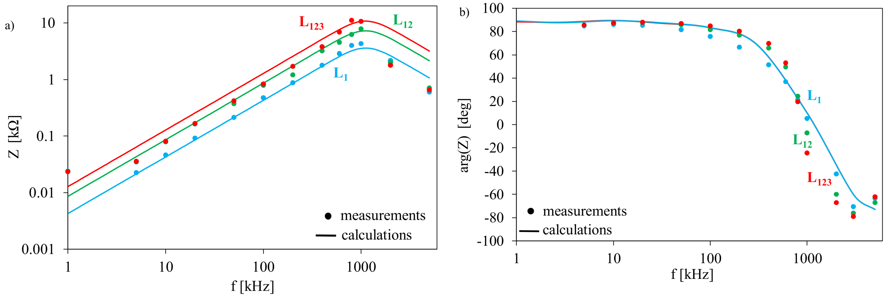
As can be seen, the resonant frequency of the considered inductor is about 1 MHz. Observing the phase of the inductor impedance, it can be seen that the impedance of the investigated device has an inductive character for frequency not exceeding 1 MHz. The influence of the winding capacitance on the impedance of the tested device was visible at a frequency f > 200 kHz. The resonance of the impedance occurred at f = 1 MHz.
Figure 10 shows the dependence of the module and phase of impedance of a single winding L
1 of the series connected two windings L
12, and the series connected three windings L
123 in the investigated inductor on frequency. The measurements were made with the value of current I
DC equal to zero.
As can be seen, the parallel resonance and its shifts into lower values of frequency were observed when connecting successive windings in a series. For two connected windings in a series, the resonant frequency was equal to 890 kHz, and for three connected windings in a series, the resonant frequency was equal to 800 kHz. Observing the phase characteristics of the inductor, it can be seen that the investigated inductor had an inductive character for a frequency not exceeding 800 kHz for L123 and 1 MHz for L1.
5.2. Results of the Computations Characteristics of a Flyback Converter
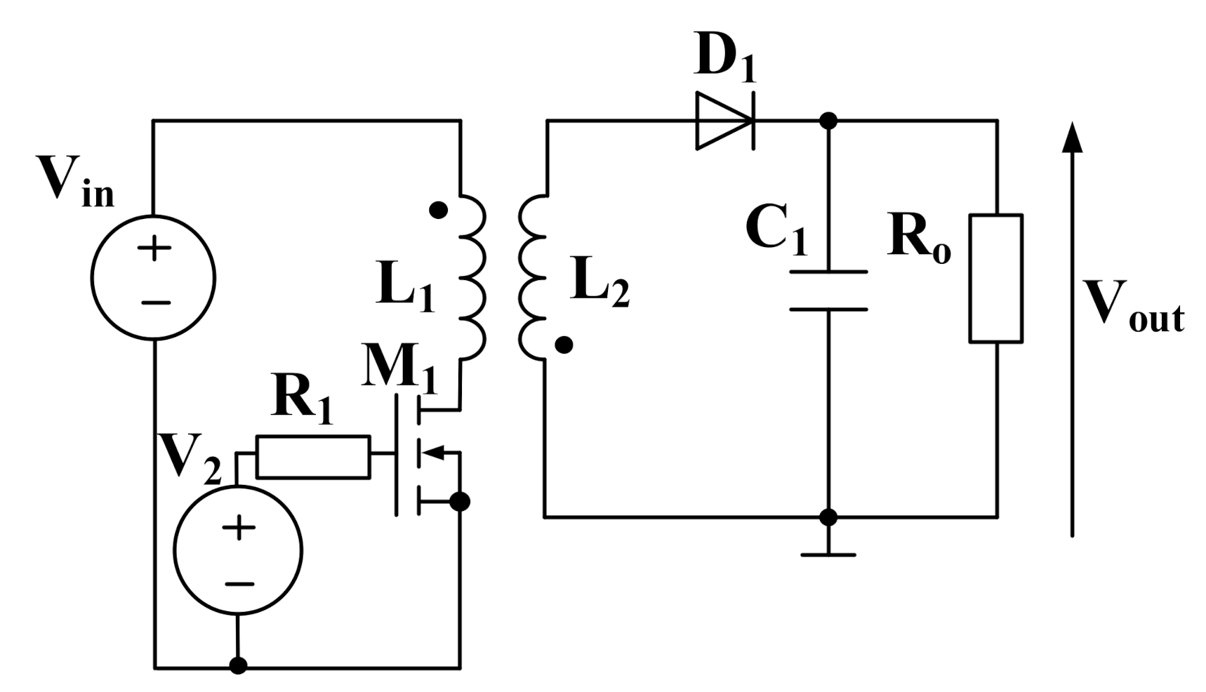
The usefulness of the developed model of the coupled inductor for the analysis of a flyback converter (shown in
Figure 11) was verified in a wide range of load resistance, R
o, and the duty cycle, d. The computations were performed for frequency, f, of the control signal equal to 200 kHz. The influence of the mentioned parameters on the value of the output voltage, V
out, of this flyback converter was investigated.
In the analyses, the following elements were used: the transistor M1 of the type IRF840, the diode D1 of the type D1N5822, the capacitor C1 = 47 µH. The number of windings of the coupled inductors L1 and L2 was the same z1 = z2 = 6. The voltage source V2 models a square wave generator with voltage levels equal to 0 and 10 V, respectively. It was assumed that the value of the input voltage Vin is equal to 12 V.
The investigations were carried out using the model described in
Section 4, and the linear model of the transformer built-in in SPICE using the KLinear component, which requires only the value of individual inductance and the value of the coupling factor. Basing the results of the measurements of the considered inductor, the value of inductance of a single inductor at I
DC = 0, A was equal to approximately 338 µH. Thus, in the computations using the linear model, it was assumed that the value of L
1 = L
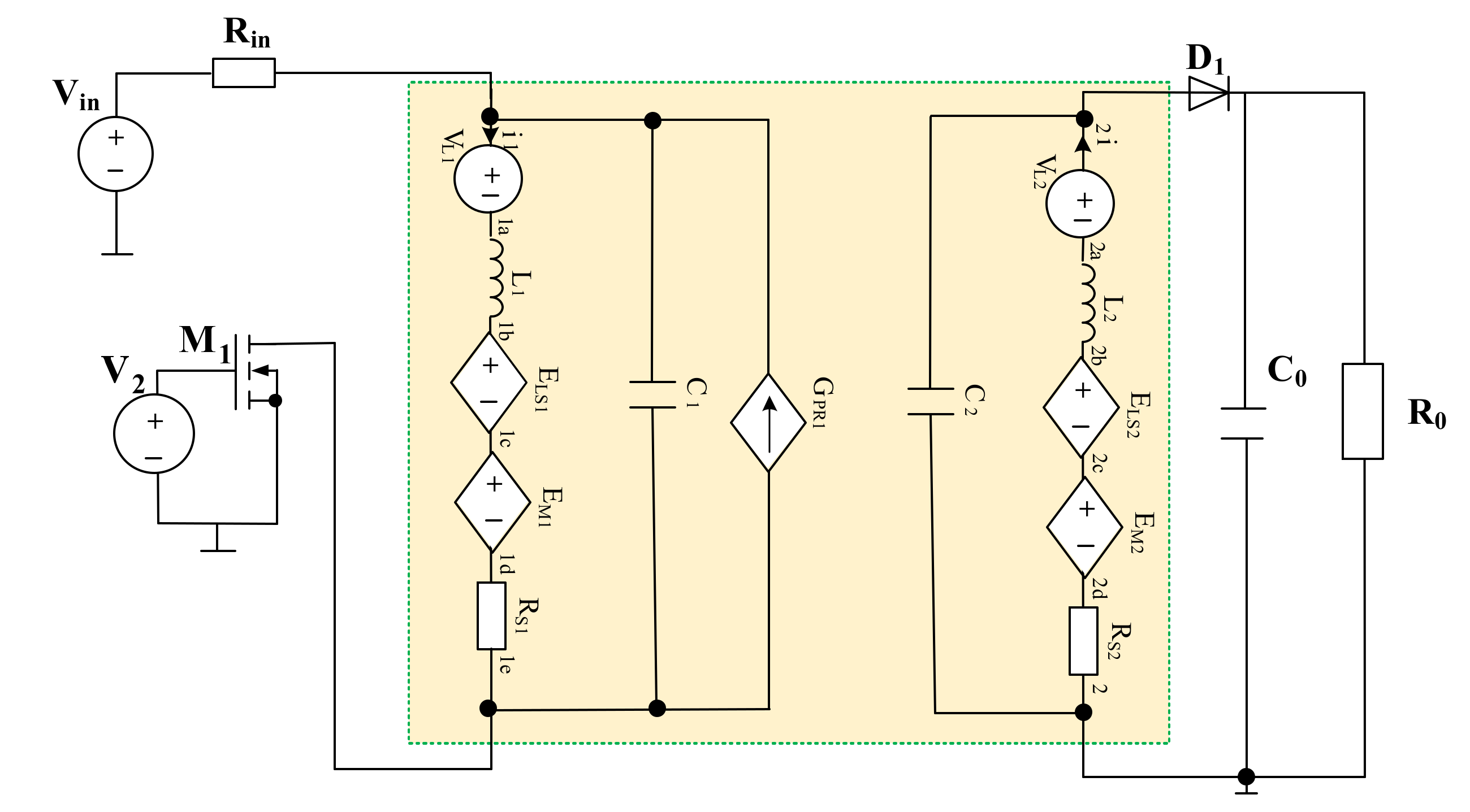
2 = 338 µH. In order to calculate the characteristics of the considered converter, the simulation circuit presented in
Figure 12 was used. For clarity the auxiliary block was omitted in this figure.
The results of computations are shown in
Figure 13 and
Figure 14. In these figures, solid lines denote the results obtained using model described in
Section 4, whereas dashed lines represent the computational results obtained using the linear model.
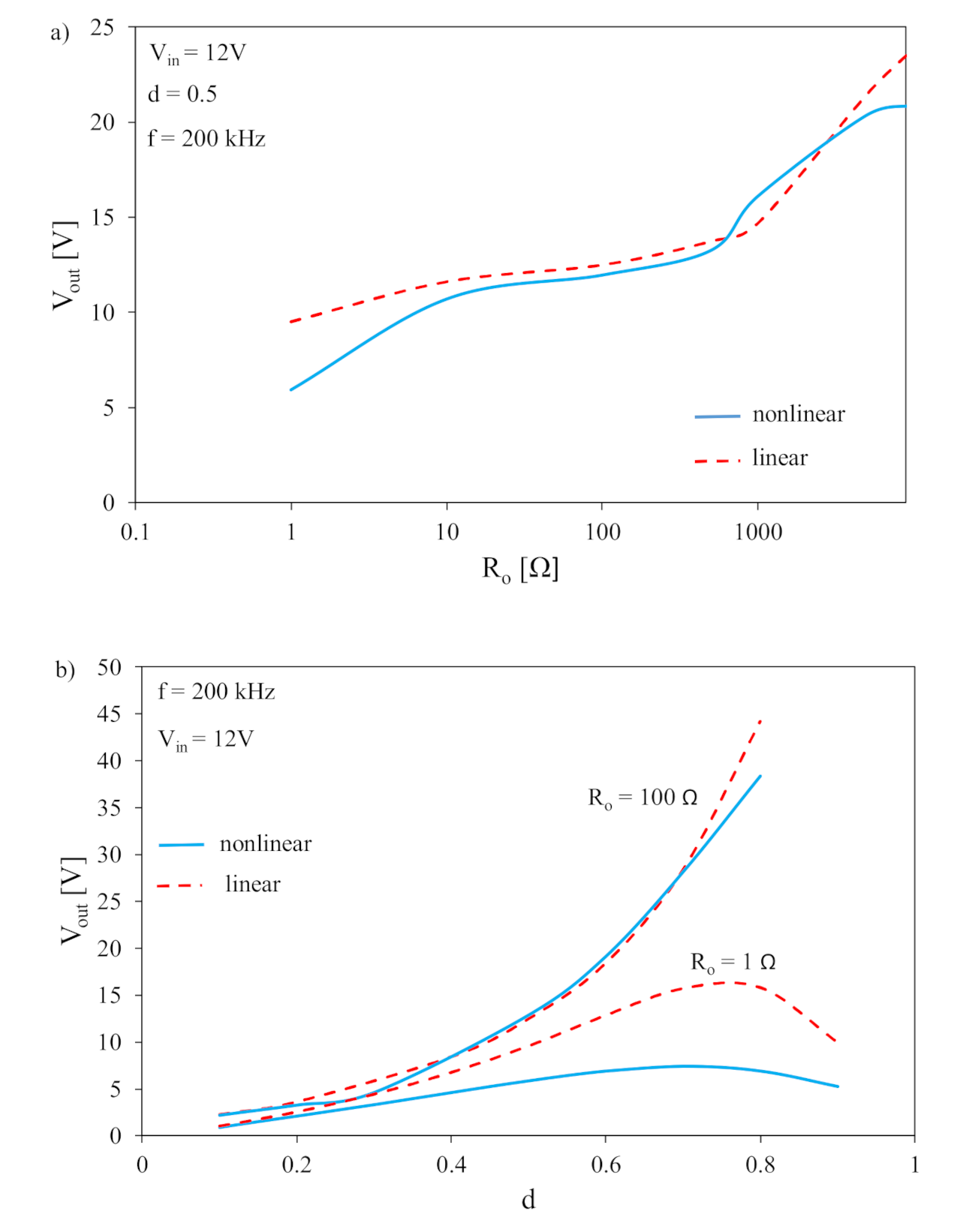
Figure 13 shows the calculated dependences of the output voltage V
out of a flyback converter on load resistance, R
0, (
Figure 13a) and on the duty cycle,
d, of the control signal (
Figure 13b).
As can be seen, an increase in load resistance, Ro, of the considered converter caused an increase in the converter output voltage value in the whole considered range of Ro from 1 to 10 kΏ. For a load resistance higher than 800 Ώ, it was observed that the converter changed the operating mode from the continuous current mode (CCM) to the discontinuous current mode (DCM). Additionally, the values of the output voltage obtained using the nonlinear model of the coupled inductor in the load resistance range from 1 to 10 Ω, and Ro > 8 kΩ, respectively, were approximately 45% and 15% lower than the value of the output voltage obtained using the linear model of the coupled inductor.
From the results of the computations presented in
Figure 13b, it can be observed that for load resistance R
o = 1 Ω, the local maximum of V
out voltage was observed for the duty cycle
d = 0.7. However, for the mentioned value of
d, the value of V
out voltage computed using the linear model was equal to about 15.8 V, whereas using the nonlinear model it was equal to approximately 6.92 V only. On the other hand, for load resistance R
o = 100 Ω, the output voltage of a flyback converter increased in function of the duty cycle of the control signal, and the greatest differences between the considered models were observed for
d > 0.65. Using the nonlinear model allowed to obtain an approximately 15% lower value of the output voltage than if using the linear model of coupled inductor.
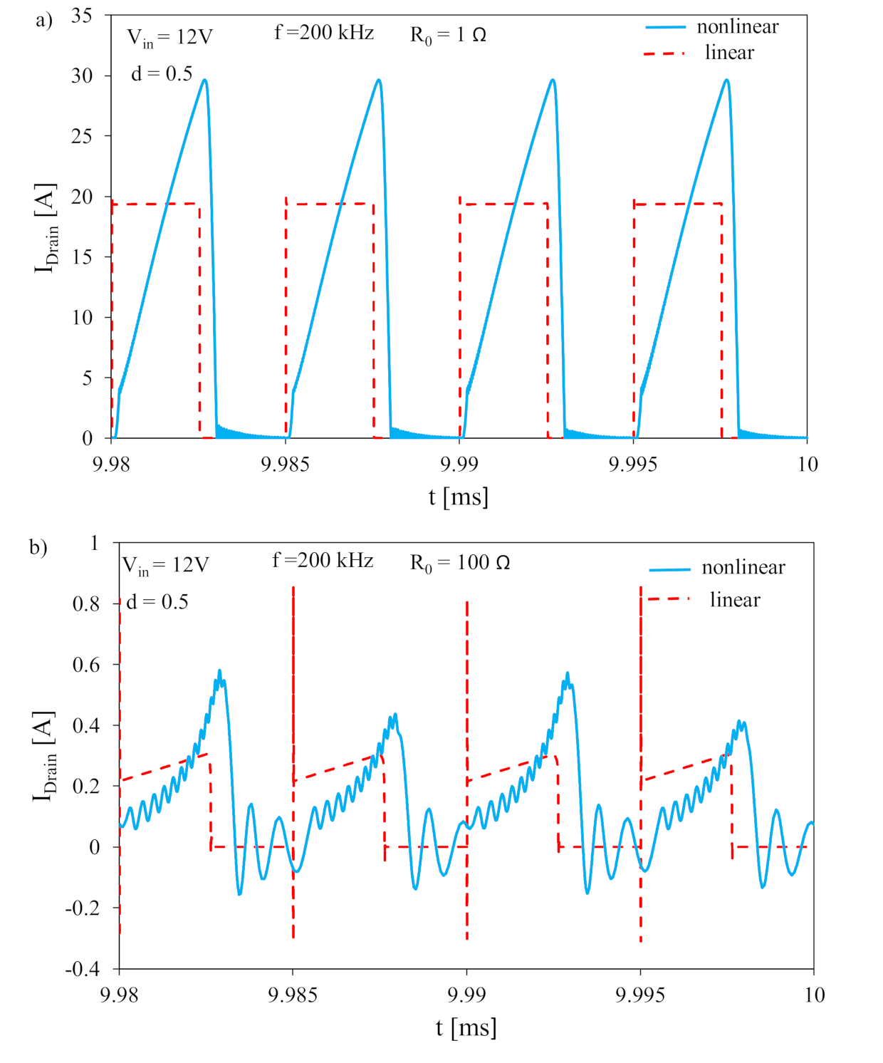
Figure 14 shows the waveforms of the drain current I
D of the transistor included in the considered converter at the steady state at load resistances equal to 1 Ω (
Figure 14a) and 100 Ω (
Figure 14b).
It is visible that for both the considered values of load resistance and the amplitude of the drain current, the results of the calculations using the nonlinear model of the coupled inductor were even approximately 50% higher than the results obtained using the linear model. Additionally, in time intervals in which the current increases, the nonlinearity of the dependence iD(t) was observed, which is a result of the nonlinear dependence of the inductor’s inductance on the current.
Additionally, in order to prove the usefulness of the conducted investigations and to take into account the nonlinear dependence of inductance of a single winding, a series connection of inductance of two windings, and inductance of a series connection of three windings on direct current, an analysis of the influence of inductances of the windings on the critical current of the boost DC–DC converter was carried out, and the obtained results are shown in
Figure 15. The values of the critical current were calculated from the dependence [
47].
where
Vin is the input voltage of the boost converter,
d is the duty cycle of the control signal,
f is the frequency of this signal, and
L is the inductance of the winding.
From the results presented in
Figure 15, it can be seen that the dependence I
CR(L) is a decreasing function of inductance. The highest values of the critical current I
CR = 4 A were obtained when the current flowed only through one winding. The series connection of two windings caused an almost two-fold reduction in the value of the critical current and a more than three-fold reduction in its value in the case of a series connection of three windings of the considered inductor. Additionally, it was observed that for inductances above 100 µH, the value of the critical current for all three considered cases was almost 100 times lower than the value of the critical current with inductance of approximately 2 µH. It can also be seen that the value of the critical current when the three windings were connected in series decreased three times compared with the value of the critical current for a single winding of the considered inductor and was equal to 13 mA for L
123. This means that the series connection of
n windings reduces the value of the critical current and may change the boost converter operating mode from discontinuous (DCM) to continuous (CCM) at a constant load.
6. Discussion
The results of the investigations presented in
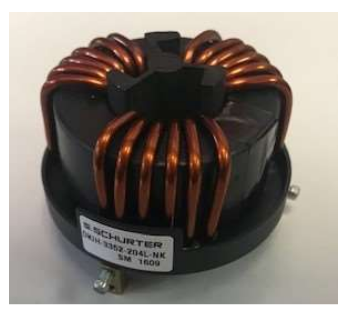
Section 5 illustrate properties of the coupled inductor and the DC–DC converters containing such an inductor. A Schurter coupled inductor, which had a nanocrystalline core on which three windings of enameled copper wire with a diameter of 2 mm was wound, was selected for the investigations.
As expected, the investigations showed that inductance of the inductor strongly depends on the direct current forced in the winding. This current was set in the range from 0 to 5 A. For a current above 5 A, the value of each of the considered inductances was constant. Additionally, the obtained results of the investigations show that ambient temperature does not influence the parameters of the investigated component. The considered inductor was also characterized by a small coupling factor, which may result in a low value of energy efficiency of power electronic systems [
1].
The results of the calculations obtained using the model proposed in the paper were in good agreement with the results of the measurements, and the mean inductance deviation between the results of the measurements and calculations was 1.87 µH, in the range of direct current from 0 to 10 A and 0.88 µH for IDC from 10 to 20 A, for which this element is dedicated.
Additionally, from the results of the calculations of a flyback converter, it was observed that the use of the linear model of the coupled inductor resulted in an approximately 45% higher value obtained for the output voltage of the considered converter in the range of low values of load resistance (1–10 Ω) and by approximately 15% for Ro > 8 kΩ. Large differences between the considered models were observed for the duty cycle, d = 0.7. In this case, the value of the output voltage obtained using nonlinear voltage was two-fold lower.
The obtained results show that the linear model of the coupled inductor generated even approximately 50% lower values of the drain current of the transistor than for the nonlinear model. The nonlinear character of L(i) dependence was observed in the waveform of the drain current obtained using the nonlinear model, and it was not observed using the linear model.
In addition, considering the usefulness of the developed model in the calculations of the boost converter and taking into account the character of the dependence of the inductance of individual windings on direct current allows for observation that the boost converter operating mode changes from the continuous (CCM) to discontinuous (DCM) mode.
It was also noticed that the value of the critical current of the boost converter strongly decreases with inductance increasing. For inductances above 100 µH, the value of the critical current for a single winding, two and three windings connected in a series, was almost 100 times lower than the value of the critical current at the inductance of approximately 2 µH. It can also be seen that the value of the critical current when three windings were connected in series was three times lower than the value of the critical current of a single winding and was equal to 13 mA. This means that increasing the number of series-connected windings reduced the critical current value and changed the boost converter mode from DCM to CCM. The investigations, the results of which are presented in this paper, can be continued towards the formulation of an electrothermal model of the coupled inductor.
7. Conclusions
The paper proposed a model of a coupled inductor. In order to verify the correctness of the proposed model, the measurements relating to the influence of frequency, direct current, and temperature on the parameters of the considered inductor were performed. Then, the obtained measurement results were compared with the results of the calculations. Additionally, to verify the usefulness of the developed model of the coupled inductor, an analysis of a flyback converter was conducted in a wide range of load resistances, Ro, and the duty cycle, d.
A significant advantage of the model is the small number of parameters and that it takes into account losses in the inductor core. The proposed model also takes into account the dependence of self and mutual inductance on direct current, frequency, and temperature.
It was also shown that the proposed model properly describes the dependences of the module and phase of the impedance of the tested device on frequency. The satisfactory accuracy was obtained for a different number of windings connected in a series and contained in the modeled device.
The proposed model may be useful for designers of power electronics systems, who at the design stage will be able to design an inductor of the appropriate value of the coupling factor, ensuring high energy efficiency of power electronics systems.


