Review

Methods of Stability Control of Perovskite Solar Cells for High Efficiency

1
Department of Solid State Physics and Nonlinear Physics, Al-Farabi Kazakh National University, IETP, Almaty 050040, Kazakhstan
2
Pediatric Faculty, Sechenov First Moscow State Medical University (Sechenov University), Moscow 119435, Russia
3
Department of Prosthetic Dentistry, Sechenov First Moscow State Medical University (Sechenov University), Moscow 119991, Russia
4
The Management Faculty, Czestochowa University of Technology, 42-201 Czestochowa, Poland
*
Author to whom correspondence should be addressed.
Energies 2021, 14(10), 2918; https://doi.org/10.3390/en14102918
Submission received: 13 April 2021 / Revised: 4 May 2021 / Accepted: 5 May 2021 / Published: 18 May 2021
(This article belongs to the Special Issue Solar Photovoltaics and Solar Thermal Energy Systems)

Abstract

:
The increasing demand for renewable energy devices over the past decade has motivated researchers to develop new and improve the existing fabrication techniques. One of the promising candidates for renewable energy technology is metal halide perovskite, owning to its high power conversion efficiency and low processing cost. This work analyzes the relationship between the structure of metal halide perovskites and their properties along with the effect of alloying and other factors on device stability, as well as causes and mechanisms of material degradation. The present work discusses the existing approaches for enhancing the stability of PSC devices through modifying functional layers. The advantages and disadvantages of different methods in boosting device efficiency and reducing fabrication cost are highlighted. In addition, the paper presents recommendations for the enhancement of interfaces in PSC structures.

1. Introduction

Halide perovskite solar cells (PSCs) are promising for practical use [1,2], due to high power conversion efficiency (PCE) of 25.5% [3,4]. Despite the variety of PSC research [5,6,7,8], PSC technology is seldom used for industrial applications, partially because of the instability of the perovskite structure layer and low reproducibility of PSCs [9,10]. The structural flaws and limited light absorption of the photoactive perovskite layer are the main factors that affect the PCE value in PSCs [11,12]. The characteristics of PSCs largely depend on the energy level alignment and carrier transport properties between the photoactive perovskite layer and carrier transport layer [11]. Therefore, most research effort is spent on surface morphology, crystallization control, energy level alignment, and conductivity of the perovskite photoactive and carrier transport layers [7]. High carrier mobility and equalization of conductivity levels promote the effective migration of photogenerated charge carriers, reducing their recombination at the interface [13,14,15]. In addition, solar modules based on PSCs are more practical and ergonomic, which inspires architects and designers to innovate when integrating these technologies into building architecture [16,17].
One way to improve the photoelectric performance and stability of perovskite devices is to enhance the quality of the perovskite light-absorbing layer by improving its structure, reducing the defects, and increasing grain sizes. This becomes possible thanks to the synergistic progress in interface modification, material synthesis, and device fabrication [18,19]. Because interfaces are decisive in charge transport and charge recombination, many studies have also focused on interface modification [20,21]. The aim of this paper is to provide an analytical review of the advances in the photovoltaics sector over the past 5 years that tackle the structure of the photoactive layer and its interfacial properties, resulting in higher stability and higher photovoltaic efficiency of PSCs.
The first section of the analytical review discusses the device architecture and work principles of PSCs. The second section looks at the latest methods for obtaining perovskite films and modifying the perovskite structure. The third section is devoted to the analysis of recent advances in the field of cathode and anode interface modification that help to improve PSC stability and efficiency. The main conclusions of the review analysis are presented in the fourth section.

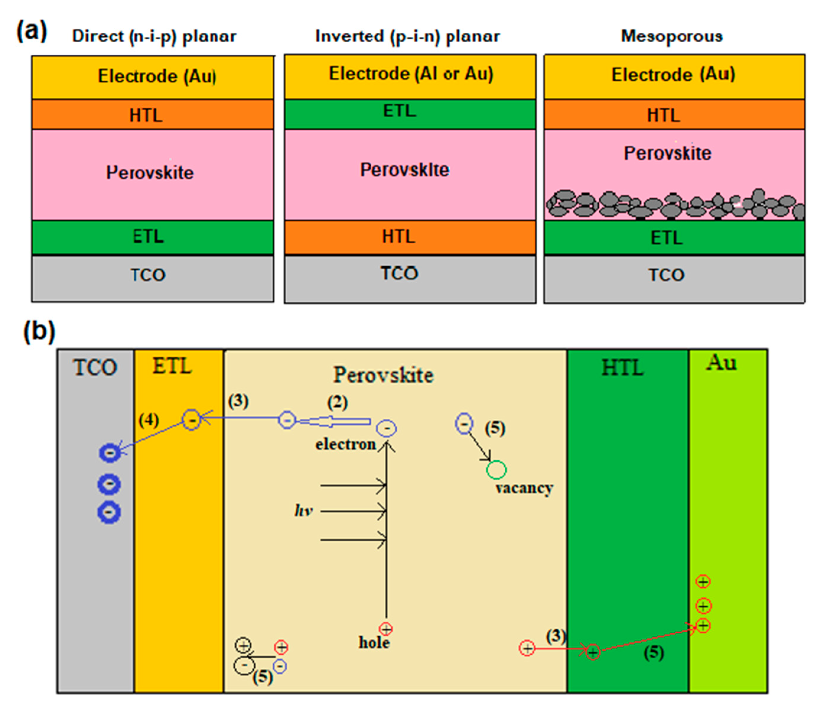
1.1. The Structure of a PSC Device

Usually, a PSC includes a perovskite light-absorbing layer that is sandwiched between a hole transport layer (HTL) and an electron transport layer (ETL). The finishing layers of cell are the transparent conductive oxide (TCO) and the metal (Au, Al) electrodes (see Figure 1a) [22].
The PSCs come in two basic structures, as depicted in Figure 1a: the planar and the mesoporous. The mesoporous structure involves a porous ETL that is usually TiO2 [24]. The planar structure is separated into two types [23]:
(1)
n-i-p configuration, where ETL (n-type semiconductor) is deposited on the TCO substrate, and HTL (p-type semiconductor) is located above the perovskite layer;
(2)
p-i-n configuration, in which HTL is deposited at TCO surface and ETL on top of the perovskite layer.
From the configuration perspective, the planar structure is the most suitable for commercialization. Mesoporous structures require high annealing temperature and processing time, which leads to an increase in cost and complexity in the production of cells [24]. Planar structures are more simplified with lower annealing temperatures and, accordingly, lower material costs. Nevertheless, the presence of hysteresis in the current-voltage characteristics and insufficient stability of cells and their lower PCE as compared to a mesoporous structure inhibit the commercialization of planar PSCs. A solution to these problems requires, among other things, an understanding of the relation between a perovskite structure and ionic compositions, as well as interface engineering [25,26].
Direct and inverted configurations differ in the polarity of the solar cell. In the direct structure, electrons are collected in the TCO electrode (Figure 1b). For inverted structure, the TCO electrode collects holes. Both configurations have good photoelectric properties and high PCE [27]; however, greater degradation of ETL is registered in inverted configurations [28]. Therefore, a direct structure is more acceptable due to better structural stability and PSC efficiency.
The chemical structure of perovskite absorbers is represented by a basic formula ABX3, where A is an organic cation (methylammonium CH3NH3+, formamidinium NH2CHNH2+, etc.) or inorganic cation (Cs+, Rb+, K+, etc.); B is a metal cation with a larger ionic radius (Pb2+, Sn2+, etc.); and X is a halide anion with a smaller ionic radius (I, Br, Cl) [29]. Depending on the composition and stoichiometry, the perovskite material exhibits a variety of crystal structures, ranging from cubic, tetragonal, or hexagonal to rhombohedral or orthorhombic phases [28,29,30].
The alignment of energy levels of perovskite at the interface with other materials that make up the device, such as the photoactive layer (perovskite) and the electrodes (anode/cathode), is a prerequisite for effective charge separation (Figure 1b) and high performance of the PSCs. The most suitable ETLs for PSC devices are low work function (WF) metal oxides (TiO2, ZnO, Ta2O5, Al2O3, ZrO2), whereas the high-WF metal oxides (MoO3, NiO, CuO, V2O5) can act as HTLs [23]. These materials are easy and inexpensive to process as compared to pure metals. The most common method for adjusting energy levels is the introduction of a dipolar layer between the perovskite and the charge transfer layers, for example, by functionalizing the surface [31]. This concept is based on changing the WF of transparent conducting oxides and the position of the Fermi level of the oxides with respect to the charge transfer levels of the semiconductor. Organic substances and salts are also widely used as interfacial layers [32,33,34,35]. For example, p-type nickel oxide (NiO) was intercalated with cesium carbonate (Cs2CO3) to function as a hole and as an electron transport layers for planar PSCs [36]. The treatment with cesium carbonate increases the energy conversion efficiency of inverted and conventional planar PSCs. Functionalization of the electron layer of ZnO with dipolar molecules improves charge transport and decreases contact resistance [37]. In addition, surface treatment with polyethylene oxide (PEO) reduces the energy level mismatch at the carbon/perovskite interface [38].
The theoretical efficiency limit of PSCs with a single-junction structure is established at 33% [39], whereas the silicon solar cells exhibit the maximum efficiency of 29.1% [40]. The certified efficiency record of PSCs is 25.5%, which is higher than that of thin film CdTe solar cells (22.1%) and polycrystalline silicon solar cells (22.3%) [41]. Due to the lower defect density, the MAPbI3 perovskite single crystals help in achieving efficient PSCs with PCE exceeding 21% [42], and the all-inorganic CsPbI3 perovskites were reported to reach a PCE over 18%. This makes them suitable for the fabrication of efficient device structures with a PCE of more than 12% [43]. The high performance of PSCs is achieved through various coating engineering approaches and the use of composite materials. Figure 2 shows the chronological progress of PCE PSCs over the last 5 years (2015–2020). Certified PCE values are compiled from data on PSC efficiency tables [44,45,46,47,48,49,50].
According to Figure 2, one can see that РСЕ value from 2015 to 2020 increased from 20.1% to 25.5%. Achievements of smooth growth of РСЕ are realized by changing the composition of the material from MAPbI3 to FAPbI3 and using their compositions to stabilize the α-phase of FAPbI3 at ambient temperature [44,45]. In addition to modifying the composition, the development of interfaces also contributes to improving PSC stability. Besides changing perovskite composition, film deposition methods play an important role in increasing PCE.
Lead-based PSCs are the most useable devices with high PCE [42,45]. However, lead toxicity and resultant chemical instability of perovskite materials are serious problems [51]. After reviewing recent studies [52], it was found that there are several scenarios for the recycling of lead from PSC waste, one of which allows the use of lead in PSCs with negligible environmental impact with others leading to a catastrophic negative impact of lead on the environment, including pollution of water and soil in landfills [53]. Currently, there are many studies [54] devoted to the search for perovskite materials based on low-toxicity elements (Sn, Bi, Sb, Ge, and Cu) or completely organic materials, which will provide alternative approaches to the implementation of high PCE and less harm to the environment in the near future.

1.2. PSC Working Principles

The capacity of PSCs to convert solar power into electricity is largely dependent on the photoactive materials properties and the device architecture. With a p-n junction photoactive material, the theoretical maximum limit of PCE approaches 33% at 1.4 eV bandgap, as shown in [55]. However, for real unijunction solar cells, the recorded efficiency is much lower than this upper limit (see Figure 3), which is explained by the influence of various factors (structural defects, impurities, etc.) [56]. As can be seen from Figure 3, the maximum PCE limit reduces as the energy bandgap shifts to 1.4 eV.
First, it was assumed that there were no losses, all photons with energy E > Eg were absorbed, and the material emitted as a black body with chemical potential μ > 0. Then it was decided to calculate the limits [55]. It was also assumed that each absorbed photon generates one electron in the external circuit, and therefore the efficiency of internal quantum equals 1. Hence, a solar cell can be considered as a body that emits blackbody radiation ϕbb and absorbs solar radiation ϕsun. The fluxes of absorbed and emitted photons are dependent on the absorbance (a(E)) that is equal to 1 for E > Eg and 0 for E < Eg. Knowing the absorbance, one can determine the short-circuit current density by solving the following equation [57]:
J s c = q E g a ( E ) ϕ s u n d E
where: E—the photon energy and q—the elementary charge.
The absorption efficiency η is defined as ratio of generated Frenkel excitons to the total number of incident photons:
η = J s c A J s c m a x
where: J s c m a x —the maximum current density that is extracted from a device. It depends on wavelength, as shown below:
J s c m a x = q h c λ 1 λ 2 P A M ( λ ) λ d λ
where: PAM—AM 1.5 G solar irradiance, h—Planck’s constant, c—the light speed in vacuum. J s c A —current density generated by the PSCs at short circuit when all the photons adsorbed within an active layer add to a photocurrent. It can be also expressed in terms of wavelength:
J s c A = q h c λ 1 λ 2 A a c t P A M ( λ ) λ d λ
where: Aact—the photoactive layer absorption.
In a real PSC, some of the absorbed solar energy is dissipated thanks to the resistance against the charge flow. Therefore, a PSC is modeled by equivalent circuit that takes this resistance into account. There are two types of resistance: series resistance, which can arise from the properties of the active layer and electrode, and contact resistance, which originates between electrodes and the active layer. It is widely accepted that for a single-junction PSC with a minimum leakage current, the current is expressed in terms of voltage:
J = J s ( exp ( q ( V J A R s ) n k B T ) ) J p h ,
where: Jph is the photogenerated current, Js—the reverse supersaturation current, n is the ideality factor determining the quality of device; and Rs is series resistance.
The first term of Equation (5) shows thermally generated currents and electrode injection current and the second term represents the photogenerated current. Using Equation (5) one can thus obtain all the necessary parameters of a solar cell [58], as well as the open circuit voltage, often expressed as:
V O C = n k B T q ln ( J p h J 0 + 1 )
When n = 1, the current recombination is insignificant in the depletion region, and diffusion current dominates in a device. When n = 2, a recombination current is prevailing. Because both the diffusion current and the recombination current within a device are known, the ideality factor will vary from 1 to 2.
The key parameters used to evaluate the quality and performance of a PSC are open circuit voltage (VOC), short-circuit current density (Jsc), fill factor (FF), and PCE. For example, in 2019, the highest recorded PCE of 24.2% was achieved with VOC = 1.1948 V, Jsc = 24.16 mA/cm2 and FF = 0.84 [49] compared to VOC = 1.059 V and FF = 0.77 and PCE value = 20.1% for 2014. Normally, the functional layers keep changing in real-life operating conditions, which leads to the emergence of various dynamic phenomena in the current–voltage curves, such as hysteresis and transient behavior [59,60].
As shown above, the energy levels of charge transport layers and crystal structure of the photoactive layer are some of the critical factors for efficient generation of photon-induced charges. The composition and morphology of the layers are also important factors. For example, the energy level alignment is sensitive to the layer thickness and can be tuned by incorporating various interface modifications of the perovskite film. The crystallinity of the perovskite layer can be controlled by using solvent additives [61]. A crucial role in thin-film solar cell fabrication is given to buffer layers or barrier layers that protect the active layers against the adverse effects of oxygen and humidity, align the energy level discrepancy between electrodes and active layers, and facilitate the charge transfer process [51]. The present review aims to study the recent modifications in the structure of the active layer and their effect on the photoelectric efficiency and PSC stability. The state-of-the-art report assesses advances in this field and can serve as a methodological guide to modifying the structure of perovskite solar cells.

2. Perovskite Structure Stability Methods

The main factor affecting the stability and efficiency of a photoelectric device is the crystallinity of the photoactive layer. It largely depends on the photoactive layer materials and methods for the preparation of the photoactive film. The alloying elements and solvent additives have been reported to improve the perovskite crystallinity [60]. This section provides a review of the novel approaches to perovskite film fabrication and improvement of the perovskite film crystallinity.

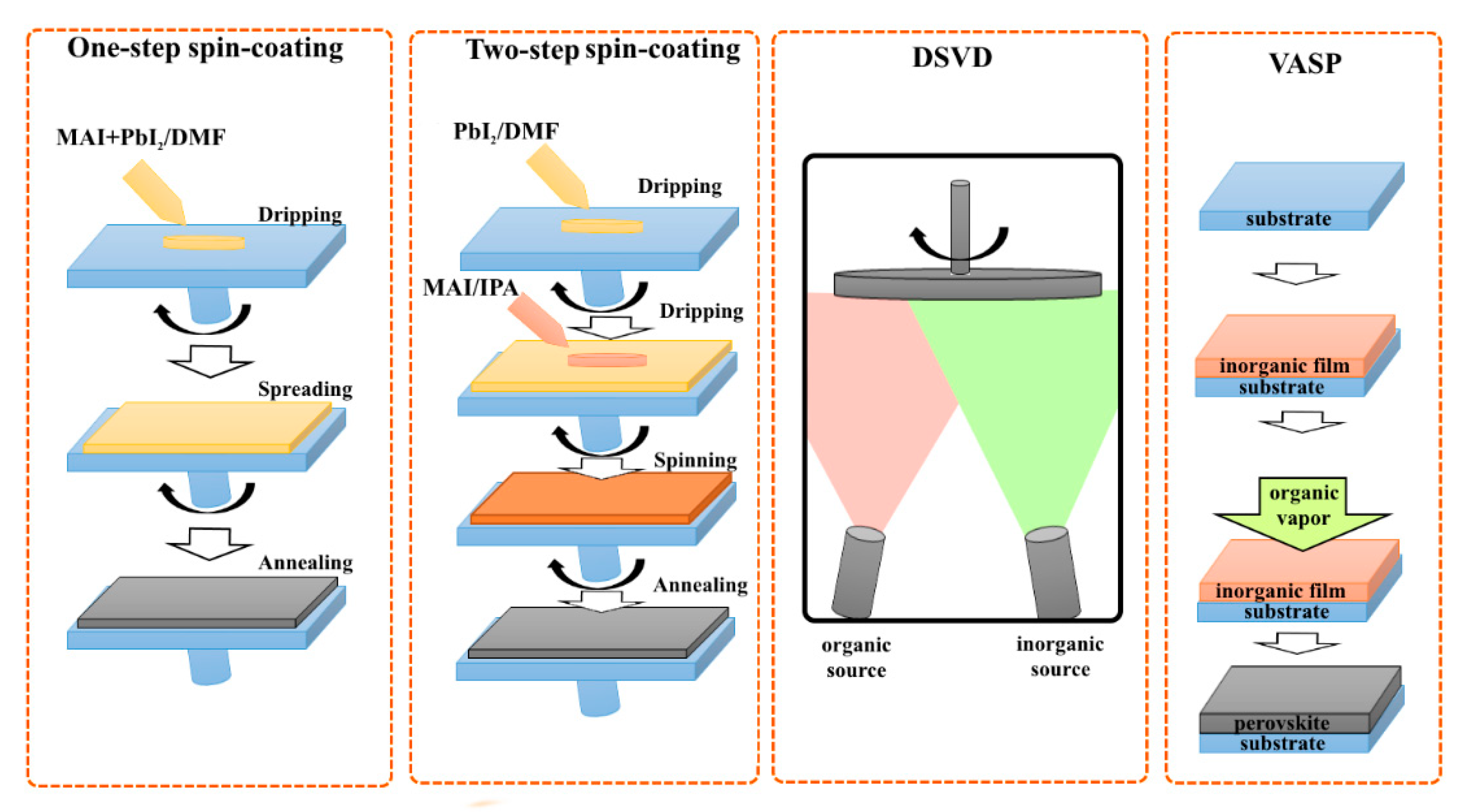
2.1. Methods for Making Perovskite Films

The core methods in perovskite film preparation are solution processing (SP) and vacuum deposition (VD). SP methods are better than VD as they are economical and compatible with the production of other active layers. To date, many options and stepwise procedures have been used in the fabrication of perovskite films, resulting in variation in both the film quality and PCE. The most commonly used VD procedures are sequential vapor deposition and dual-source VD processes. In SP, the most popular methods are single-step spin coating, two-step spin coating, vacuum deposition, and vapor-assisted solution processing (VASP) (Figure 4). Below is a description of the features of each of the popular methods for producing perovskite film with an assessment of the advantages and disadvantages of each.
The single-step spin-coating process involves the dissolving of organic halide molecules and metal halide for perovskite crystals. For this, CH3NH3I (MAI), CH3NH3Cl (MACl), or NH2CHNH2I (FAI) are mixed with PbI2 in C3H7NO (DMF), (CH3)2SO (DMSO), or C4H6O2 (GBL). Once the mixing is complete, it is deposited onto the substrate by spin coating and annealed at 90 °C (Figure 4) [61]. Using this method, however, film properties such as morphology and uniformity are difficult to control [6]. The perovskite films produced in such a way typically possess enlarged crystal grains and rough film morphologies, which can lead to the suppression of the carrier extraction processes in the PSC device. However, using an anti-solvent dripping technique during spin-coating, the perovskite precursor solution results in pure and stable crystal phases of polycrystalline perovskite films with highly reproducible efficiencies of more than 22% [62]. This method is quite simple and affordable, and the high quality of the film mainly depends on the purity of the precursors and the quality of the substrate [63].
In the two-step spin-coating process, PbI2 is deposited onto the substrate, then MAI undergoes spin coating on dried PbI2 film. The film color changes from yellow to brown. The film is then annealed at 90 °C for 10 min to enhance film morphology [64]. Sometimes, instead of the second step, the PbI2 film is immersed into the organic salt solution [65]. The two-step method was developed to improve and control the morphology of the film in MAI deposition. It involves the diffusion of cations (CH3NH3) into the PbI2 matrix with the formation of a perovskite film. The main disadvantage of this method is that it produces a dense film (MAPbI3) on the top PbI2 layer, preventing the perovskite formation within the PbI2 layer. To overcome this, one will need larger film thickness and more time [66]. The use of this technique also guarantees a high cell performance with high values of photovoltaic characteristics, namely Jsc, VOC, and FF.
The VD methods allow the precursor deposition in a vacuum at low temperatures. Multiple simultaneous precursor depositions or deposition of one precursor at a time is possible. The advantage of VD is that it improves the purity of the resulting material and reduces contamination from solvents, which makes it possible to control thickness and uniformity of a film. The low temperature of fabrication allows the use of various types of substrates, i.e., textiles and flexible substrates. DSVD produces high-density perovskite films of arbitrary thickness that can be controlled in real time [67,68]. However, this method is more expensive compared to other methods when obtaining similar cell performance metrics (Table 1).
The vapor-assisted solution processing (VASP) method is a stepwise procedure in which a PbI2 film is precipitated from the solution by centrifugation and then placed in a chamber filled with CH3NH3I vapor at 150 °C for two hours, which saturates the PbI2 matrix with CH3NH3 [69]. The perovskite film obtained by using this method is dense and shows no sign of current leakage. It also exhibits a uniform morphology, which helps to reduce the scattering of charge carriers, thereby improving device performance and charge recombination. The advantages of VASP are that high-purity films are highly reproducible and compatible with large areas; there is accurate control over film morphology and thickness and high PCE (>19%) [67,68,69] (Table 1).
Table 1. Photoelectric properties of perovskite-based devices fabricated using different deposition methods.
PerovskiteDeposition MethodPCE, %Jsc, mA/cm2Voc, VFFReference
MAI-PbI2Single-step deposition19.5023.401.0877.00[61]
MAI-PbI2Single-step deposition24.8226.351.1680.90[6]
MAI-PbI2-DMSOSingle-step deposition19.7123.81.0876.20[70]
MAI-PbI2Two-step sequential deposition20.1323.811.1076.75[64]
MAI-PbI2Two-step sequential deposition19.2723.481.1273.66[65]
FA-PbI3Two-step sequential deposition22.424.41.1778.89[66]
MAI-PbI2Vacuum deposition19.423.111.0977[67]
MAI-PbI2Vacuum deposition19.124.31.1579.8[68]
FA1–xMAxPbI3Vacuum deposition18.822.51.175.1[71]
(FAPbI3xMACl)/DMF⋅NMPVapor-assisted solution processing19.7824.791.0774.60[72]
FA-PbI3Vapor-assisted solution processing21.425.21.1277.5[73]
MAI-PbI2Vapor-assisted solution processing19.4620.891.1680.4[74]
It seems that the one- and two-step depositions are the best ways to achieve the highest PCE (Table 1), and the vapor deposition creates better uniformity and density of the film in comparison with SP method. Vapor deposition produced films do not have holes that cause performance-reducing current leakage. Films produced by DSVD exhibit higher photocurrent and open circuit voltage due to better uniformity and fewer impurities. However, the two-step solution-based sequential deposition is more preferable in terms of device fabrication cost [66].
In addition to the above methods, there are other alternative technologies. For example, in recent years, the method of contactless inkjet printing has gained popularity. This technology offers the deposition of layers with simultaneous control of the structure of printed perovskite solar cells [75]. The results of [76] showed that the method of inkjet printing makes it possible to control the thickness of the perovskite layer in the range of 175 to 780 nm, which in turn makes it possible to control the morphology of the structure by adjusting the distance between the drops of the inkjet printer cartridge. In addition, according to the test results, printed solar cells based on Сs0,1(FA-MA)0.9Pb(IxBrx−1)3 demonstrate РСЕ 12.9%, which represents a significant improvement over similar formulations obtained by other methods (Table 1). One of the latest alternative technologies for the production of hybrid perovskite solar cells is blade-coating, which also makes it possible to control the layer thickness [77]. However, unlike the previous methods, the crystallization process of the perovskite film strongly depends on the method and conditions of coating. The results of studying the MAPbI3 perovskite obtained by the blade-coating method showed [78] that the morphology and composition of the coatings are determined by the rate of solvent removal. This, in turn, affects the РСЕ value, which reaches up to 15%. In another work, it was shown [79] that a PSC with an area of 1.96 cm2 obtained by this method is capable of reaching РСЕ of up to 18.3%, which is less than the efficiencies for films obtained by two-step sequential deposition (Table 1). Study of the features of film crystallization processes with alternative methods of preparation is ongoing, and understanding these processes can significantly expand their future possibilities for large-scale production of perovskite solar cells [80].

2.2. Additives for Enhanced Crystallinity

In addition to choosing deposition methods, it is possible to enhance the perovskite film crystallinity and morphology using a variety of additives. Dai et al. [81] hold that the incorporation of a few solvent additives to the perovskite precursor solution improves film crystallinity and device performance. Polar aprotic solvents are widely used when preparing MAI solutions and lead halides (see Section 1). Some organic solvents, such as C6H5Cl, C6H5, and C₈H₁₀, are an excellent choice for conducting organic polymers and buffer layer materials, even though they exhibit poor solubility [82].
The integration of acetonitrile (ACN) in the FAI/MABr/MACl precursor by sequential deposition for Cs/FA/MA perovskite films has been reported to reduce surface defects, improve the crystal grain size, and enhance device efficiency from 13.06% to 15.64% [83]. In addition, ACN-containing devices showed more stable behavior in air, thermal, and humidity stability tests.
The DMF additives were reported to positively affect the morphology of MAPbI3 perovskite films [84,85,86]. When introducing methyl ammonium chloride (MACl) and DMF as co-additives in a two-step sequential process, the polar solvent facilitates easy penetration of MAI into the PbI2 layer [85], and MAC1 induces MAPbI3 to crystallize in the pure α-phase. The result of the synergistic effect between these two additives is a pure α-phase perovskite film, with uniform morphology, enhanced VOC = 1.181 V, and PCE = 19.02%. Oseni et al. [87] show that the use of DMSO instead of DMF for the creation of the first PbI2 layer in a two-stage processing method provides smoother films with uniform sized grains and reduced PbI2 residue.
Arias-Ramos et al. [88] report that using a mixture of ethyl acetate (EA) and 4-tert-butylpyridine (tBP) as an anti-solvent in the preparation of CH3NH3PbI3 perovskite film at high relative humidity of approximately 60% contributes to the formation of perovskite surface with improved uniformity and higher hydrophobic capacity. The presence of tBP in EA enables the device to reach 18.04% of PCE and retain over 80% of its initial efficiency after 180 days of storage in high humidity conditions.
Perovskite films fabricated from the CH3NH3PbI3xClx perovskite precursor solution containing 1-chloronaphthalene (CN) additive were reported to be smoother and more uniform with fewer pinholes and voids and with better surface coverage as compared to conventional films [89]. Bis(trifluoromethane)sulfonimide lithium salt (Li-TFSI) is often used as a p-dopant to increase the concentration of holes in the Spiro-MeOTAD layer and gain higher PCE. PSCs fabricated with spiro(TFSI) 2 show enhanced stability in an inert atmosphere [89].
The above findings suggest that improvements to film deposition technology and the use of various additives enhance film morphology, resulting in better stability and efficiency of the device.

3. Impact of Interface Modification on PSC Performance

As noted in Section 1, another channel for PCE losses in PSCs is often found at the interface between the extracting layers and perovskite surface, which leads to charge carrier recombination. PSC surface recombination velocity depends on the surface state, which can be 2.9 cm/s for high-purity perovskite single crystals [90]. However, in polycrystalline perovskite films with inhomogeneous morphology and insignificant levels of traps, surface recombination is substantial in charge extraction and device efficiency [91]. Hence, the interfacial modifications in PSCs define the processes of charge extraction and transport, thereby determining the overall performance of the operational device. To this end, they mainly seek to achieve an effective passivation of surface traps with inhibited surface recombination. For this, it is important that the interfaces between the photoactive and charge transporting layers (ETL and HTL) allow for the passivation of surface traps and suppression of charge carrier recombination. The present review focuses on the new front-end approaches to the surface trap passivation from the past 5 years.
When fabricating PSCs by thermal annealing, sites may form near the film surface region, occupied by either halide or metal ions. The undersaturated surface ions originating as a result of this process are a trapping center and migrate under electric field action, resulting in a loss of charge carriers and VOC. So far, considerable work has been conducted to obtain an effective surface trap passivation through incorporating interlayers [92].

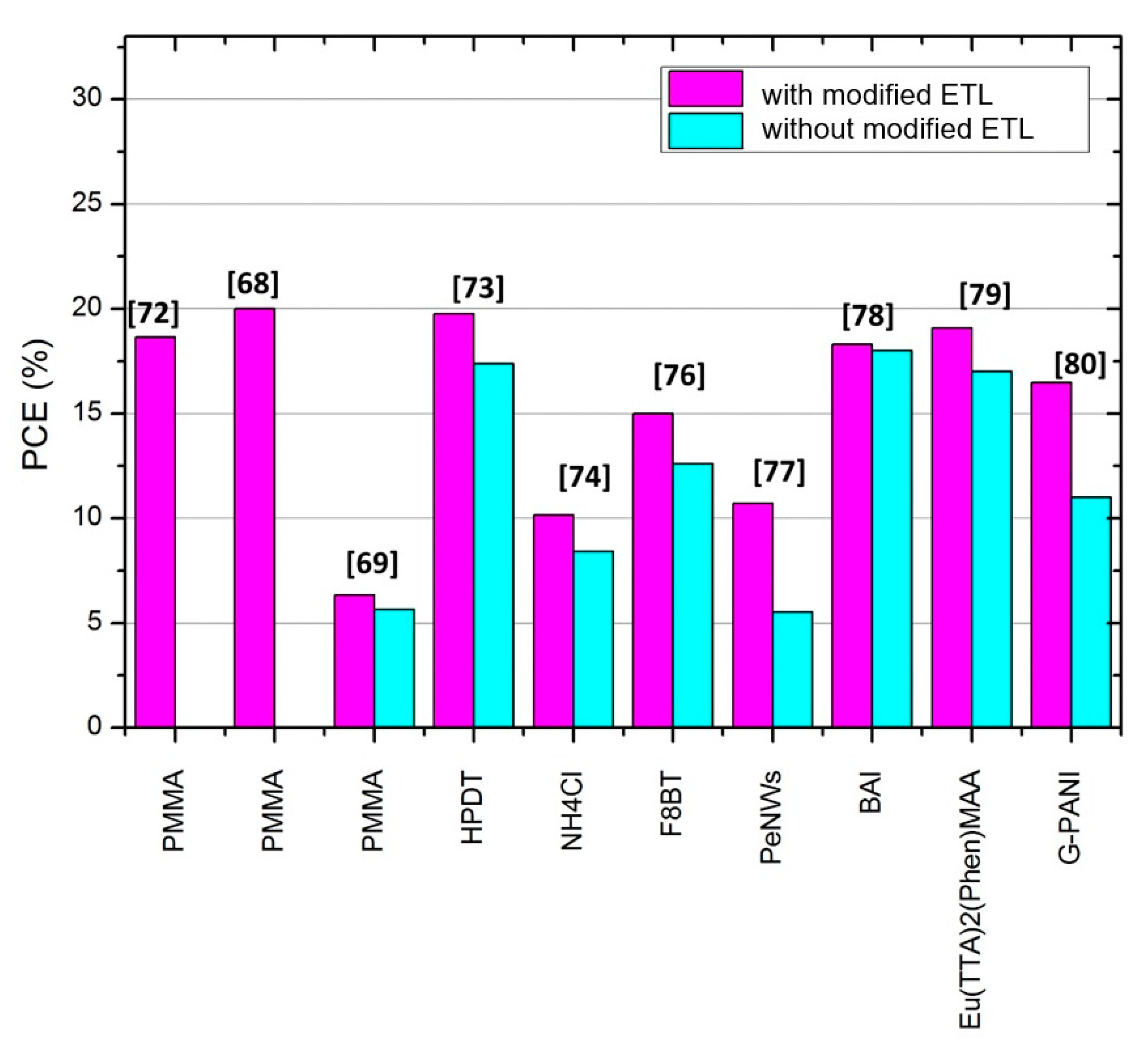
3.1. ETLs Interfacial Modifications

In PSCs with p-i-n device structure, the most common ETLs are those based on fullerene derivatives, such as PCBM, which can improve electron collection and passivate electron traps. However, fullerene’s passivation ability seems inefficient. Therefore, a polymer polymethyl methacrylate (PMMA) was integrated into the PCBM matrix to enhance film quality and trap passivation [93]. By optimizing concentration and molecular weight of PMMA, the PSCs can reach 30% efficiency. The incorporation of PMMA additives was reported to affect the surface potential of PCBM and reduce charge recombination losses, as well as space charge effects [94,95]. In addition, the PMAA additive promotes the formation of a dense and uniform morphology with fewer surface traps. Such features enhance the reliability and stability of the ETL, as well as the protection of the active perovskite layer. For example, a PMMA/PCBM mixture with a ratio of 1:2 promotes the effective defect passivation at the interface between the ETL and triple-cation perovskite (Cs0.05 (FA0.85MA0.15)0.95Pb (I0.85Br0.15)3), thereby increasing VOC to 1.17 V and PCE to 18.63%. This method improves the stability of PSCs and helps to retain 82% of its initial efficiency after 768 h of storage at room temperature [96].
Some research efforts were devoted to introducing a trace of NH4Cl to the sol–gel-derived ZnO precursor to reduce ZnO film WF, tune perovskite film surface morphology, and thus suppress trap state density in CsPbIBr2 films [97]. The resultant CsPbIBr2 films were characterized by the presence of high crystallinity and micron-size grains. For optimal NH4Cl-modified ZnO, a dramatic improvement in VOC from 1.08 to 1.27 V strengthened the efficiency of CsPbIBr2 PSC to 10.16%, the highest value among pure-CsPbIBr2 PSCs at a low fabrication temperature of 160 °C. Furthermore, NH4Cl-modified ZnO ETL was reported to significantly reduce hysteresis and improve device stability [97].
The introduction of sodium heparin (HS) at the MAPbI3/TiO2 interface was reported to increase trap passivation and device stability [98]. The incorporated HS layer also reduced the hydrophobicity of TiO2 and the number of pinholes within the TiO2 layer. These modifications lead to higher perovskite crystallinity. The HS interfacial layer enables the device to maintain 85% of its initial efficiency after 70 days of storage in ambient condition.
The interface modification of ETL improves the perovskite film morphology and increases trap passivation, resulting in higher PCE (Figure 5). The maximum efficiencies correspond to devices containing a PMMA-modified PCBM layer. PSCs modified with organic semiconductors, such as an n-type organic molecule, a homologous perylenediimide tetramer (HPDT), a n-butylamine iodide (BAI), or down conversion materials, for example Eu(TTA)2(Phen)MAA, also exhibit high performances.

3.2. Interfacial Modifications in НTLs

The commonly used materials for HTLs are small organic molecules and polymers with tailorable WFs and surface properties, such as poly (3,4-ethylenedioxythiophene) polystyrene sulfonate (PEDOT:PSS) [104]. So far, considerable work has been conducted on strategies that facilitate charge extraction at the HTL/perovskite interface through the introduction of additives, buffer layers, etc. Various conductive polymers (PTAA, P3HT, PCBTDPP, etc.) and conjugated polyelectrolytes (PEDOT:PSS, P3CT, CPE-K, etc.) are used as HTLs in PSCs because of their benefits in reducing fabrication and processing costs [105]. However, the interface modification of HTL increases trap passivation. Typically, HTLs are both organic and inorganic materials.
Xu et al. [106] proposed a novel method for HTL modification that uses copper (I) thiocyanate (CuSCN) as a dopant for PEDOT:PSS. The resulting film had larger crystals, and the PCE increased to 15.3% with an open circuit voltage of more than 1.0 V. The long-term device stability also improved. This suggests that the doping of CuSCN in PEDOT:PSS HTLs is an effective way to obtain stable high-performance PSCs. The PEDOT:PSS layer can also be modified with vanadium pentoxide (V2O5) [107]. The V2O5 modified layer averts the acidic PEDOT:PSS film from etching the ITO electrode and maintains the PSC structure stability. The 4.7-diphenyl-1.10-phenanthroline (Bphen) modified layer was reported to prevent the photoactive layer film from direct connection with the Ag electrode, which improved the storage stability of the device. With this method, the PCE rose from 11.08% to 15.49%. Another widely used HTL in PSC structures is NiOx. Lian et al. [108] modified the NiOx layer with different polymers, namely polystyrene, poly (methyl methacrylate) (PMMA), and poly[bis(4-phenyl)(2,4,6-trimethylphenyl)amine] (PTAA) to optimize the NiOx/perovskite interface. As a result, PSCs with modified PMMA and PTAA films achieved high VOC values of up to 1.19 V and high conversion efficiencies of 21.56%, the highest values possible. In some cases, HTLs can be enhanced with the 3-(cyclohexylamino)-2-hydroxy-1-propanesulfonic acid (CAPSO) [109], NiOx nanoparticles [110], Cu1.8S nanoparticles [111], etc., leading to better performances and longer lifetime.

4. Conclusions

This paper presents a detailed report on the progress made in perovskite solar cells so far along with changes in device performances and the challenges of perovskite fabrication to create a better understanding of the problem and assist in the search for new fabrication techniques. It seems that the major challenges in the development of PSCs are currently associated with the insufficient stability of PSC devices, reproducibility of device fabrication, and fabrication costs, which hinder commercialization. Unstable interfaces between the active layers cause the degradation of photoactive materials and lower device performance. PSC structure can be stabilized by modifying the perovskite layers and interfaces. The photoelectric properties of the PSC device were found to be dependent on the film deposition technique, and the use of various additives improves film morphology and crystallinity. Another PSC research prospect is interfacial layer selection. The incorporation of inorganic and organic materials as interfacial layers promotes the effective passivation of surface traps and charges collection from a photoactive medium to relevant electrodes. The fullerene PCBM modified by depositing PMMA polymeric additives appears to be an excellent choice in the preparation of ETLs, while the modified PEDOT:PSS is the best fit for use as HTLs.

Author Contributions

Conceptualization, A.M. and D.F.; methodology, V.S. and G.Z.; formal analysis, A.M. and S.K.; investigation, D.F., V.S. and G.Z.; resources, V.S.; data curation, A.M.; writing—original draft preparation, D.F., V.S. and G.Z.; writing—review and editing, A.M. and S.K.; visualization, V.S. All authors have read and agreed to the published version of the manuscript.

Funding

This research received no external funding.

Institutional Review Board Statement

Not applicable.

Informed Consent Statement

Not applicable.

Data Availability Statement

All data will be available on request.

Acknowledgments

This work was supported by Al-Farabi Kazakh National University, Institute of Experimental & Theoretical Physics, AP08855457 project “Development of an innovative technology for producing nanocrystalline composite coatings for fuel cell electrodes and hydrogen energy”.

Conflicts of Interest

The authors declare no conflict of interest.

References

  1. Yang, J.; Bao, Q.; Shen, L.; Ding, L. Potential applications for perovskite solar cells in space. Nano Energy 2020, 1, 05019. [Google Scholar] [CrossRef]
  2. Yu, Z.; Hagfeldt, A.; Sun, L. The application of transition metal complexes in hole-transporting layers for perovskite solar cells: Recent progress and future perspectives. Coordin. Chem. Rev. 2020, 406, 213143. [Google Scholar] [CrossRef]
  3. Kim, J.Y.; Lee, J.W.; Jung, H.S.; Shin, H.; Park, N.G. High-efficiency perovskite solar cells. Chem. Rev. 2020, 120, 7867–7918. [Google Scholar] [CrossRef]
  4. Fang, Z.; Zeng, Q.; Zuo, C.; Zhang, L.; Xiao, H.; Cheng, M.; Hao, F.; Bao, Q.; Zhang, L.; Wu, W.-Q.; et al. Perovskite-based tandem solar cells. Sci. Bull. 2020, 1, 1–7. [Google Scholar] [CrossRef]
  5. Wu, J.; Li, Y.; Tan, S.; Yu, B.; Li, H.; Li, Y.; Shi, J.; Wu, H.; Luo, Y.; Li, D.; et al. Enhanced perovskite solar cell efficiency via the electric-field-induced approach. ACS Appl. Mater. Interfaces 2020, 12, 27258–27267. [Google Scholar] [CrossRef] [PubMed]
  6. Jeong, M.; Choi, I.W.; Go, E.M.; Cho, Y.; Kim, M.; Lee, B.; Yang, C. Stable perovskite solar cells with efficiency exceeding 24.8% and 0.3-V voltage loss. Science 2020, 369, 1615–1620. [Google Scholar] [CrossRef] [PubMed]
  7. Zheng, X.; Hou, Y.; Bao, C.; Yin, J.; Yuan, F.; Huang, Z.; Sing, K.; Liu, J.; Zhou, C.H.; Lin, Y.; et al. Managing grains and interfaces via ligand anchoring enables 22.3%-efficiency inverted perovskite solar cells. Nat. Energy 2020, 5, 131–140. [Google Scholar] [CrossRef]
  8. Park, N.G. Research direction toward scalable, stable, and high efficiency perovskite solar cells. Adv. Energy Mater. 2020, 10, 1903106. [Google Scholar] [CrossRef]
  9. Ghosh, S.; Singh, T. Role of ionic liquids in organic-inorganic metal halide perovskite solar cells efficiency and stability. Nano Energy 2019, 63, 103828. [Google Scholar] [CrossRef]
  10. Deng, K.; Chen, Q.; Li, L. Modification engineering in SnO2 electron transport layer toward perovskite solar cells: Efficiency and stability. Adv. Funct. Mater. 2020, 30, 2004209. [Google Scholar] [CrossRef]
  11. Luo, D.; Su, R.; Zhang, W.; Gong, Q.; Zhu, R. Minimizing non-radiative recombination losses in perovskite solar cells. Nat. Rev. Mater. 2020, 5, 44–60. [Google Scholar] [CrossRef]
  12. Gao, F.; Zhao, Y.; Zhang, X.; You, J. Recent progresses on defect passivation toward efficient perovskite solar cells. Adv. Energy Mater. 2020, 10, 1902650. [Google Scholar] [CrossRef]
  13. Domanski, K.; Alharbi, E.A.; Hagfeldt, A.; Grätzel, M.; Tress, W. Systematic investigation of the impact of operation conditions on the degradation behaviour of perovskite solar cells. Nat. Energy 2018, 3, 61–67. [Google Scholar] [CrossRef]
  14. Shaimenova, A.; Ilyassova, G.; Klyuyeva, Y.; Khashimova, A. Development of the Institution of Arbitration in Kazakhstan: Problems of Theory and Practice. J. Adv. Res. Law Econ. 2020, 11, 169–186. [Google Scholar] [CrossRef]
  15. Nan, G.; Zhang, X.; Lu, G. Self-healing of photocurrent degradation in perovskite solar cells: The role of defect-trapped excitons. J. Phys. Chem. Lett. 2019, 10, 7774–7780. [Google Scholar] [CrossRef]
  16. Lucchi, E.; Lopez, C.P.; Franco, G. A conceptual framework on the integration of solar energy systems in heritage sites and buildings. IOP Conf. Ser. Mater. Sci. Eng. 2020, 949, 012113. [Google Scholar] [CrossRef]
  17. Sánchez-Pantoja, N.; Vidal, R.; Pastor, M.C. EU-Funded Projects with actual implementation of renewable energies in cities. Analysis of their concern for aesthetic impact. Energies 2021, 14, 1627. [Google Scholar] [CrossRef]
  18. Chen, B.; Song, J.; Dai, X.; Liu, Y.; Rudd, P.N.; Hong, X.; Huang, J. Synergistic effect of elevated device temperature and excess charge carriers on the rapid light-induced degradation of perovskite solar cells. Adv. Mater. 2019, 31, 1902413. [Google Scholar] [CrossRef]
  19. Seok, S.I.; Grätzel, M.; Park, N.G. Methodologies toward highly efficient perovskite solar cells. Small 2018, 14, 1704177. [Google Scholar] [CrossRef] [PubMed]
  20. Correa-Baena, J.P.; Saliba, M.; Buonassisi, T.; Grätzel, M.; Abate, A.; Tress, W.; Hagfeldt, A. Promises and challenges of perovskite solar cells. Science 2017, 358, 739–744. [Google Scholar] [CrossRef] [Green Version]
  21. Sun, X.; Shao, Z.; Rao, Y.; Meng, H.; Gao, C.; Chen, C.; Liu, D.; Lv, P.; Li, Z.; Wang, X.; et al. A low-temperature additive-involved leaching method for highly efficient inorganic perovskite solar cells. Adv. Energy Mater. 2021, 11, 2002754. [Google Scholar] [CrossRef]
  22. Hima, A.; Lakhdar, N.; Benhaoua, B.; Saadoune, A.; Kemerchou, I.; Rogti, F. An optimized perovskite solar cell designs for high conversion efficiency. Superlatt. Microstruct. 2019, 129, 240–246. [Google Scholar] [CrossRef]
  23. Bi, S.; Leng, X.; Li, Y.; Zheng, Z.; Zhang, X.; Zhang, Y.; Zhou, H. Interfacial modification in organic and perovskite solar cells. Adv. Mater. 2019, 31, 1805708. [Google Scholar] [CrossRef]
  24. Tsindeliani, I.; Egorova, M.; Vasilyeva, E.; Bit-Shabo, I.; Kikavets, V. Collection of Taxes from Ultimate Beneficiaries: Russian Regulatory Model. Account. Econ. Law 2021, 1–24. [Google Scholar] [CrossRef]
  25. Ren, H.; Yu, S.; Chao, L.; Xia, Y.; Sun, Y.; Zuo, S.; Huang, W. Efficient and stable Ruddlesden–Popper perovskite solar cell with tailored interlayer molecular interaction. Nat. Photon. 2020, 14, 154–163. [Google Scholar] [CrossRef]
  26. Ono, L.K.; Qi, Y.; Liu, S.F. Progress toward stable lead halide perovskite solar cells. Joule 2018, 2, 1961–1990. [Google Scholar] [CrossRef] [Green Version]
  27. Sherafatipour, G.; Benduhn, J.; Patil, B.R.; Ahmadpour, M.; Spoltore, D.; Rubahn, H.G.; Vandewal, K.; Madsen, M. Degradation pathways in standard and inverted DBP-C 70 based organic solar cells. Sci. Rep. 2019, 9, 1–11. [Google Scholar] [CrossRef] [Green Version]
  28. Gautier, R.; Massuyeau, F.; Galnon, G.; Paris, M. Lead halide post-perovskite-type chains for high-efficiency white-light emission. Adv. Mater. 2019, 31, 1807383. [Google Scholar] [CrossRef]
  29. Ito, N.; Kamarudin, M.A.; Hirotani, D.; Zhang, Y.; Shen, Q.; Ogomi, Y.; Hayase, S. Mixed Sn–Ge perovskite for enhanced perovskite solar cell performance in air. J. Phys. Chem. Lett. 2018, 9, 1682–1688. [Google Scholar] [CrossRef]
  30. Pitchaiya, S.; Natarajan, M.; Santhanam, A.; Asokan, V.; Yuvapragasam, A.; Ramakrishnan, V.M.; Velauthapillai, D. A review on the classification of organic/inorganic/carbonaceous hole transporting materials for perovskite solar cell application. Arab. J. Chem. 2020, 13, 2526–2557. [Google Scholar] [CrossRef]
  31. Tao, L.; Wang, B.; Wang, H.; Chen, C.; Ding, X.; Tian, Y.; Lu, H.; Yang, X.; Cheng, M. Surface defect passivation and energy level alignment engineering with a fluorine-substituted hole transport material for efficient perovskite solar cells. ACS Appl. Mater. Interfaces 2021, 13, 13470–13477. [Google Scholar] [CrossRef] [PubMed]
  32. Liu, N.; Yam, C. First-principles study of intrinsic defects in formamidinium lead triiodide perovskite solar cell absorbers. Phys. Chem. 2018, 20, 6800–6804. [Google Scholar] [CrossRef]
  33. Xiao, Z.; Yan, Y. Progress in theoretical study of metal halide perovskite solar cell materials. Adv. Energy Mater. 2017, 7, 1701136. [Google Scholar] [CrossRef]
  34. Xu, Q.; Yang, D.; Lv, J.; Sun, Y.Y.; Zhang, L. Perovskite solar absorbers: Materials by design. Small Methods 2018, 2, 1700316. [Google Scholar] [CrossRef]
  35. Hussain, I.; Tran, H.P.; Jaksik, J.; Moore, J.; Islam, N.; Uddin, M.J. Functional materials, device architecture, and flexibility of perovskite solar cell. Emerg. Mater. 2018, 1, 133–154. [Google Scholar] [CrossRef] [Green Version]
  36. Singh, M.; Yang, R.T.; Weng, D.W.; Hu, H.; Singh, A.; Mohapatra, A.; Chen, Y.-T.; Lu, Y.-J.; Guo, T.-F.; Li, G.; et al. Low-temperature processed bipolar metal oxide charge transporting layers for highly efficient perovskite solar cells. Sol. Energy Mater. Sol. Cells 2021, 221, 110870. [Google Scholar] [CrossRef]
  37. Zhang, X.; Sun, Y.; Wang, M.; Cui, H.; Xie, W.; Shen, L.; Guo, W. Facilitating electron collection of organic photovoltaics by passivating trap states and tailoring work function. Sol. Energy 2019, 181, 9–16. [Google Scholar] [CrossRef]
  38. Wu, Z.; Liu, Z.; Hu, Z.; Hawash, Z.; Qiu, L.; Jiang, Y.; Ono, L.K.; Qi, Y. Highly efficient and stable perovskite solar cells via modification of energy levels at the perovskite/carbon electrode interface. Adv. Mater. 2019, 31, 1804284. [Google Scholar] [CrossRef] [PubMed]
  39. Park, N.G.; Segawa, H. Research direction toward theoretical efficiency in perovskite solar cells. ACS Photon. 2018, 5, 2970–2977. [Google Scholar] [CrossRef]
  40. Yoshikawa, K.; Kawasaki, H.; Yoshida, W.; Irie, T.; Konishi, K.; Nakano, K.; Uto, T.; Adachi, D.; Kanematsu, M.; Uzu, H.; et al. Silicon heterojunction solar cell with interdigitated back contacts for a photoconversion efficiency over 26%. Nat. Energy 2017, 2, 17032. [Google Scholar] [CrossRef]
  41. National Renewable Energy Laboratory (NREL). Research-Cell Efficiency Chart. Champion Module Efficiency Chart. Available online: https://www.nrel.gov/pv/module-efficiency.html (accessed on 27 October 2019).
  42. Chen, Z.; Turedi, B.; Alsalloum, A.Y.; Yang, C.; Zheng, X.; Gereige, I.; AlSaggaf, A.; Mohammed, O.F.; Bakr, O.M. Single-crystal MAPbI3 perovskite solar cells exceeding 21% power conversion efficiency. ACS Energy Lett. 2019, 4, 1258–1259. [Google Scholar] [CrossRef] [Green Version]
  43. Wang, Y.; Dar, M.I.; Ono, L.K.; Zhang, T.; Kan, M.; Li, Y.; Zhao, Y. Thermodynamically stabilized β-CsPbI3–based perovskite solar cells with efficiencies > 18%. Science 2019, 365, 591–595. [Google Scholar] [CrossRef] [PubMed]
  44. Green, M.A.; Emery, K.; Hishikawa, Y.; Warta, W.; Dunlop, E.D. Solar cell efficiency tables (Version 46). Prog. Photovolt. 2015, 23, 1–9. [Google Scholar] [CrossRef]
  45. Green, M.A.; Emery, K.; Hishikawa, Y.; Warta, W.; Dunlop, E.D. Solar cell efficiency tables (Version 48). Prog. Photovolt. 2016, 24, 905–913. [Google Scholar] [CrossRef] [Green Version]
  46. Green, M.A.; Hishikawa, Y.; Dunlop, E.D.; Levi, D.H.; HohlEbinger, J.; Ho-Baillie, A.W.Y. Solar cell efficiency tables (Version 51). Prog. Photovolt. 2018, 26, 3–12. [Google Scholar] [CrossRef] [Green Version]
  47. Green, M.A.; Hishikawa, Y.; Dunlop, E.D.; Levi, D.H.; HohlEbinger, J.; Yoshita, M.; Ho-Baillie, A.W.Y. Solar cell efficiency tables (Version 53). Prog. Photovolt. 2019, 27, 3–12. [Google Scholar] [CrossRef] [Green Version]
  48. Green, M.A.; Dunlop, E.D.; Levi, D.H.; Hohl-Ebinger, J.; Yoshita, M.; Ho-Baillie, A.W.Y. Solar cell efficiency tables (Version 54). Prog. Photovolt. 2019, 27, 565–575. [Google Scholar] [CrossRef]
  49. Green, M.A.; Dunlop, E.D.; Hohl-Ebinger, J.; Yoshita, M.; Kopidakis, N.; Ho-Baillie, A.W.Y. Solar cell efficiency tables (Version 55). Prog. Photovolt. 2020, 28, 3–15. [Google Scholar] [CrossRef]
  50. Green, M.A.; Dunlop, E.D.; Hohl-Ebinger, J.; Yoshita, M.; Hao, X. Solar cell efficiency tables (version 57). Prog. Photovolt. 2021, 29, 3–15. [Google Scholar] [CrossRef]
  51. Xing, G.; Mathews, N.; Sun, S.; Lim, S.S.; Lam, Y.M.; Grätzel, M.; Mhaisalkar, S.; Sum, T.C. Long-range balanced electron-and hole-transport lengths in organic-inorganic CH3NH3PbI3. Science 2013, 342, 344–347. [Google Scholar] [CrossRef] [PubMed]
  52. Ke, W.; Kanatzidis, M.G. Prospects for low-toxicity lead-free perovskite solar cells. Nat. Commun. 2019, 10, 965. [Google Scholar] [CrossRef]
  53. Pobedinsky, V.; Shestak, V. Improving Environmental Legislation in Central Asia. Environ. Policy Law 2020, 50, 69–79. [Google Scholar] [CrossRef]
  54. Katsuba, S.; Shestak, V.; Kvasnikova, T.; Bokov, Y. Liability for Violation of Environmental Legislation in the EU. Eur. Energy Environ. Law Rev. 2021, 30, 9–19. [Google Scholar]
  55. Shockley, W.; Queisser, H.J. Detailed balance limit of efficiency of p-n junction solar cells. J. Appl. Phys. 1961, 32, 510–519. [Google Scholar] [CrossRef]
  56. Kazmerski, L.L. Solar photovoltaics R&D at the tipping point: A 2005 technology overview. J. Electron. Spectrosc. Related Phenom. 2006, 150, 105–135. [Google Scholar]
  57. Wu, F.; Pathak, R.; Chen, K.; Wang, G.; Bahrami, B.; Zhang, W.H.; Qiao, Q. Inverted current–voltage hysteresis in perovskite solar cells. ACS Energy Lett. 2018, 3, 2457–2460. [Google Scholar] [CrossRef] [Green Version]
  58. Mahmood, K.; Sarwar, S.; Mehran, M.T. Current status of electron transport layers in perovskite solar cells: Materials and properties. RSC Adv. 2017, 7, 17044–17062. [Google Scholar] [CrossRef] [Green Version]
  59. Qarony, W.; Hossain, M.I.; Salleo, A.; Knipp, D.; Tsang, Y.H. Rough versus planar interfaces: How to maximize the short circuit current of perovskite single and tandem solar cells. Mater. Today Energy 2019, 11, 106–113. [Google Scholar] [CrossRef]
  60. Xing, G.; Wu, B.; Wu, X.; Li, M.; Du, B.; Wei, Q.; Guo, J.; Yeow, E.K.L.; Sum, T.C.; Huang, W. Transcending the slow bimolecular recombination in lead-halide perovskites for electroluminescence. Nat. Commun. 2017, 8, 14558. [Google Scholar] [CrossRef] [Green Version]
  61. Wang, F.; Zhang, T.; Wang, Y.; Liu, D.; Zhang, P.; Chen, H.; Ji, L.; Chen, L.; Chen, Z.D.; Wu, J.; et al. Correction: Steering the crystallization of perovskites for high-performance solar cells in ambient air. J. Mater. Chem. A 2020, 8, 18387. [Google Scholar] [CrossRef]
  62. Konstantakou, M.; Perganti, D.; Falaras, P.; Stergiopoulos, T. Anti-solvent crystallization strategies for highly efficient perovskite solar cells. Crystals 2017, 7, 291. [Google Scholar] [CrossRef] [Green Version]
  63. Ermanova, I.; Yaghoobi Nia, N.; Lamanna, E.; Di Bartolomeo, E.; Kolesnikov, E.; Luchnikov, L.; Di Carlo, A. Crystal engineering approach for fabrication of inverted perovskite solar cell in ambient conditions. Energies 2021, 14, 1751. [Google Scholar] [CrossRef]
  64. Sun, H.; Deng, K.; Zhu, Y.; Liao, M.; Xiong, J.; Li, Y.; Li, L. A novel conductive mesoporous layer with a dynamic two-step deposition strategy boosts efficiency of perovskite solar cells to 20%. Adv. Mater. 2018, 30, 1801935. [Google Scholar] [CrossRef] [PubMed]
  65. Zhao, Y.; Zhang, X.; Han, X.; Hou, C.; Wang, H.; Qi, J.; Zhang, Q. Tuning the reactivity of PbI2 film via monolayer Ti3C2Tx MXene for two-step-processed CH3NH3PbI3 solar cells. Chem. Eng. J. 2020, 127912. [Google Scholar]
  66. Lee, D.G.; Kim, D.H.; Lee, J.M.; Kim, B.J.; Kim, J.Y.; Shin, S.S.; Jung, H.S. High efficiency perovskite solar cells exceeding 22% via a photo-assisted two-step sequential deposition. Adv. Funct. Mater. 2020, 2006718. [Google Scholar]
  67. Tavakoli, M.M.; Tavakoli, R. All-vacuum-processing for fabrication of efficient, large-scale, and flexible inverted perovskite solar cells. Rapid Res. Lett. 2021, 15, 2000449. [Google Scholar] [CrossRef]
  68. Kim, B.S.; Gil-Escrig, L.; Sessolo, M.; Bolink, H.J. Deposition kinetics and compositional control of vacuum-processed CH3NH3PbI3 perovskite. J. Phys. Chem. Lett. 2020, 11, 6852–6859. [Google Scholar] [CrossRef] [PubMed]
  69. Zhu, R.; Wei, X.; Xie, G.; Simon, T.; Cui, T. Numerical simulation of vapor deposition process of perovskite solar cells: The influence of MAI vapor flow to perovskite growth. J. Solar Energy Eng. 2020, 143, 011002. [Google Scholar] [CrossRef]
  70. Ahn, N.; Son, D.Y.; Jang, I.H.; Kang, S.M.; Choi, M.; Park, N.G. Highly reproducible perovskite solar cells with average efficiency of 18.3% and best efficiency of 19.7% fabricated via Lewis base adduct of lead (II) iodide. J. Am. Chem. Soc. 2015, 37, 8696–8699. [Google Scholar] [CrossRef]
  71. Gil-Escrig, L.; Dreessen, C.; Kaya, I.C.; Kim, B.S.; Palazon, F.; Sessolo, M.; Bolink, H.J. Efficient vacuum-deposited perovskite solar cells with stable cubic FA1–x MA x PbI3. ACS Energy Lett. 2020, 5, 3053–3061. [Google Scholar] [CrossRef]
  72. Wang, D.; Wu, C.; Luo, W.; Guo, X.; Qi, X.; Zhang, Y.; Zhang, Z.; Qu, B.; Xiao, L.; Chen, Z. Glass rod-sliding and low pressure assisted solution processing composition engineering for high-efficiency perovskite solar cells. Sol. Energy Mater. Sol. Cells 2020, 211, 110532. [Google Scholar] [CrossRef]
  73. Lu, H.; Liu, Y.; Ahlawat, P.; Mishra, A.; Tress, W.R.; Eickemeyer, F.T.; Grätzel, M. Vapor-assisted deposition of highly efficient, stable black-phase FAPbI3 perovskite solar cells. Science 2020, 370, eabb8985. [Google Scholar] [CrossRef] [PubMed]
  74. Liu, Z.; Meng, K.; Wang, X.; Qiao, Z.; Xu, Q.; Li, S.; Cheng, L.; Li, Z.; Chen, G. In situ observation of vapor-assisted 2D–3D heterostructure formation for stable and efficient perovskite solar cells. Nano Lett. 2020, 20, 1296–1304. [Google Scholar] [CrossRef] [PubMed]
  75. Liang, C.; Li, P.; Gu, H.; Zhang, Y.; Li, F.; Song, Y.; Shao, G.; Mathews, N.; Xing, G. One-step inkjet printed perovskite in air for efficient light harvesting. Solar Rrl 2018, 2, 1700217. [Google Scholar] [CrossRef]
  76. Mathies, F.; Eggers, H.; Richards, B.S.; Hernandez-Sosa, G.; Lemmer, U.; Paetzold, U.W. Inkjet-printed triple cation perovskite solar cells. ACS Appl. Energy Mater. 2018, 1, 1834–1839. [Google Scholar] [CrossRef]
  77. Wang, Z.; Zeng, L.; Zhang, C.; Lu, Y.; Qiu, S.; Wang, C.; Liu, C.; Pan, L.; Wu, S.; Hu, J.; et al. Rational interface design and morphology control for blade-coating efficient flexible perovskite solar cells with a record fill factor of 81%. Adv. Funct. Mater. 2020, 30, 2001240. [Google Scholar] [CrossRef]
  78. Zhong, Y.; Munir, R.; Li, J.; Tang, M.C.; Niazi, M.R.; Smilgies, D.M.; Zhao, S.; Amassian, A. Blade-coated hybrid perovskite solar cells with efficiency > 17%: An in situ investigation. ACS Energy Lett. 2018, 3, 1078–1085. [Google Scholar] [CrossRef]
  79. Li, C.; Yin, J.; Chen, R.; Lv, X.; Feng, X.; Wu, Y.; Cao, J. Monoammonium porphyrin for blade-coating stable large-area perovskite solar cells with > 18% efficiency. J. Am. Chem. Soc. 2019, 141, 6345–6351. [Google Scholar] [CrossRef]
  80. Pelle, M.; Lucchi, E.; Maturi, L.; Astigarraga, A.; Causone, F. Coloured BIPV technologies: Methodological and experimental assessment for architecturally sensitive areas. Energies 2020, 13, 4506. [Google Scholar] [CrossRef]
  81. Dai, T.; Li, X.; Zhang, Y.; Xu, D.; Geng, A.; Zhao, J.; Chen, X. Performance improvement of polymer solar cells with binary additives induced morphology optimization and interface modification simultaneously. Solar Energy 2020, 201, 330–338. [Google Scholar] [CrossRef]
  82. Yang, D.; Grott, S.; Jiang, X.; Wienhold, K.S.; Schwartzkopf, M.; Roth, S.V.; Müller-Buschbaum, P. In situ studies of solvent additive effects on the morphology development during printing of bulk heterojunction films for organic solar cells. Small Methods 2020, 4, 2000418. [Google Scholar] [CrossRef]
  83. Hussein, H.T.; Zamel, R.S.; Mohamed, M.S.; Mohammed, M.K. High-performance fully-ambient air processed perovskite solar cells using solvent additive. J. Phys. Chem. Solids 2021, 149, 109792. [Google Scholar] [CrossRef]
  84. Lee, S.; Tang, M.C.; Munir, R.; Barrit, D.; Kim, Y.J.; Kang, R.; Kim, D.Y. In situ study of the film formation mechanism of organic–inorganic hybrid perovskite solar cells: Controlling the solvate phase using an additive system. J. Mater. Chem. 2020, 8, 7695–7703. [Google Scholar] [CrossRef]
  85. Hou, M.; Xu, Y.; Tian, Y.; Wu, Y.; Zhang, D.; Wang, G.; Zhang, X. Synergistic effect of MACl and DMF towards efficient perovskite solar cells. Org. Electron. 2021, 88, 106005. [Google Scholar] [CrossRef]
  86. Wang, Q.; Zhang, W.; Zhang, Z.; Liu, S.; Wu, J.; Guan, Y.; Han, H. Crystallization control of ternary-cation perovskite absorber in triple-mesoscopic layer for efficient solar cells. Adv. Energy Mater. 2020, 10, 1903092. [Google Scholar] [CrossRef]
  87. Oseni, S.O.; Mola, G.T. The effect of uni-and binary solvent additives in PTB7: PC61BM based solar cells. Solar Energy 2017, 150, 66–72. [Google Scholar] [CrossRef]
  88. Arias-Ramos, C.F.; Kumar, Y.; Abrego-Martínez, P.G.; Hu, H. Efficient and stable hybrid perovskite prepared at 60% relative humidity with a hydrophobic additive in anti-solvent. Solar Energy Mater. Solar Cells 2020, 215, 110625. [Google Scholar] [CrossRef]
  89. Song, X.; Wang, W.; Sun, P.; Ma, W.; Chen, Z.K. Additive to regulate the perovskite crystal film growth in planar heterojunction solar cells. Appl. Phys. Lett. 2015, 106, 033901. [Google Scholar] [CrossRef]
  90. Nukusheva, A.; Ilyassova, G.; Rustembekova, D.; Zhamiyeva, R.; Arenova, L. Global warming problem faced by the international community: International legal aspect. Int. Environ. Agreem. Pol. Law Econ. 2020, 1–15. [Google Scholar] [CrossRef]
  91. Bai, Y.; Meng, X.; Yang, S. Interface engineering for highly efficient and stable planar p-i-n perovskite solar cells. Adv. Energy Mater. 2018, 8, 1701883. [Google Scholar] [CrossRef]
  92. Chen, J.; Park, N.G. Materials and methods for interface engineering toward stable and efficient perovskite solar cells. ACS Energy Lett. 2020, 5, 2742–2786. [Google Scholar] [CrossRef]
  93. Bett, A.J.; Schulze, P.S.; Winkler, K.M.; Kabakli, Ö.S.; Ketterer, I.; Mundt, L.E.; Goldschmidt, J.C. Two-terminal Perovskite silicon tandem solar cells with a high-Bandgap Perovskite absorber enabling voltages over 1.8 V. Prog. Photovolt. 2020, 28, 99–110. [Google Scholar] [CrossRef] [Green Version]
  94. Ferdowsi, P.; Ochoa-Martinez, E.; Alonso, S.S.; Steiner, U.; Saliba, M. Ultrathin polymeric films for interfacial passivation in wide band-gap perovskite solar cells. Sci. Rep. 2020, 10, 22260. [Google Scholar] [CrossRef] [PubMed]
  95. Tan, Y.; Xiang, B.; Zou, T.; Liu, C.; Wang, K.; Chen, J.; Zhou, H. Optimization of PMMA: PCBM interlayer for MAPbI 3/IGZO phototransistor. In Proceedings of the 2020 4th IEEE Electron Devices Technology & Manufacturing Conference (EDTM), Penang, Malaysia, 6–21 April 2020; pp. 1–3. [Google Scholar]
  96. Hu, X.; Wang, H.; Wang, M.; Zang, Z. Interfacial defects passivation using fullerene-polymer mixing layer for planar-structure perovskite solar cells with negligible hysteresis. Solar Energy 2020, 206, 816–825. [Google Scholar] [CrossRef]
  97. Wang, H.; Cao, S.; Yang, B.; Li, H.; Wang, M.; Hu, X.; Zang, Z. NH4Cl-modified ZnO for high-performance CsPbIBr2 perovskite solar cells via low-temperature process. Solar Rrl 2020, 4, 1900363. [Google Scholar] [CrossRef]
  98. You, S.; Wang, H.; Bi, S.; Zhou, J.; Qin, L.; Qiu, X.; Tang, Z. A biopolymer heparin sodium interlayer anchoring TiO2 and MAPbI3 enhances trap passivation and device stability in perovskite solar cells. Adv. Mater. 2018, 30, 1706924. [Google Scholar] [CrossRef]
  99. Jiang, M.; Niu, Q.; Tang, X.; Zhang, H.; Xu, H.; Huang, W.; Xia, R. Improving the performances of perovskite solar cells via modification of electron transport layer. Polymers 2019, 11, 147. [Google Scholar] [CrossRef] [PubMed] [Green Version]
  100. Zhao, F.; Deng, L.; Wang, K.; Han, C.; Liu, Z.; Yu, H.; Hu, B. Surface modification of SnO2 via MAPbI3 nanowires for a highly efficient non-fullerene acceptor-based organic solar cell. ACS Appl. Mater. Interfaces 2020, 12, 5120–5127. [Google Scholar] [CrossRef]
  101. Zou, Y.; Cui, Y.; Wang, H.Y.; Cai, Q.; Mu, C.; Zhang, J.P. Highly efficient and stable 2D–3D perovskite solar cells fabricated by interfacial modification. Nanotechnology 2019, 30, 275202. [Google Scholar] [CrossRef]
  102. Bi, W.; Wu, Y.; Zhang, B.; Jin, J.; Li, H.; Liu, L.; Song, H. Enhancing photostability of perovskite solar cells by Eu (TTA) 2 (Phen) MAA interfacial modification. ACS Appl. Mater. Interfaces 2019, 11, 11481–11487. [Google Scholar] [CrossRef]
  103. Mohseni, H.R.; Dehghanipour, M.; Dehghan, N.; Tamaddon, F.; Ahmadi, M.; Sabet, M.; Behjat, A. Enhancement of the photovoltaic performance and the stability of perovskite solar cells via the modification of electron transport layers with reduced graphene oxide/polyaniline composite. Solar Energy 2021, 213, 59–66. [Google Scholar] [CrossRef]
  104. Rong, B.; Jin, S.; Chen, X.; Wei, Y.; Fang, Y.; Zhao, Y.; Wu, J. Improving the efficiency of perovskite solar cells by additive engineering with ditetrabutylammonium dichromate. Org. Electron. 2020, 85, 105845. [Google Scholar] [CrossRef]
  105. Ali, J.; Li, Y.; Gao, P.; Hao, T.; Song, J.; Zhang, Q.; Liu, F. Interfacial and structural modifications in perovskite solar cells. Nanoscale 2020, 12, 5719–5745. [Google Scholar] [CrossRef] [PubMed]
  106. Xu, L.; Li, Y.; Zhang, C.; Liu, Y.; Zheng, C.; Lv, W.; Chen, R. Improving the efficiency and stability of inverted perovskite solar cells by CuSCN-doped PEDOT:PSS. Solar Energy Mater. Solar Cells 2020, 206, 110316. [Google Scholar] [CrossRef]
  107. Liu, Z.; He, T.; Wang, H.; Song, X.; Liu, H.; Yang, J.; Ma, H. Improving the stability of the perovskite solar cells by V2O5 modified transport layer film. RSC Adv. 2017, 7, 18456–18465. [Google Scholar] [CrossRef] [Green Version]
  108. Lian, X.; Chen, J.; Shan, S.; Wu, G.; Chen, H. Polymer modification on the NiO x hole transport layer boosts open-circuit voltage to 1.19 V for perovskite solar cells. ACS Appl. Mater. Interfaces 2020, 12, 46340–46347. [Google Scholar] [CrossRef] [PubMed]
  109. Zhao, Z.; Yuan, L.; Huang, J.; Shi, J.; Cao, Y.; Zi, W.; Zhang, W. Modified HTL-induced efficiency enhancement for inverted perovskite solar cells. Org. Electron. 2020, 78, 105557. [Google Scholar] [CrossRef]
  110. Jin, Z.; Guo, Y.; Yuan, S.; Zhao, J.S.; Liang, X.M.; Qin, Y.; Ai, X.C. Modification of NiO x hole transport layer for acceleration of charge extraction in inverted perovskite solar cells. RSC Adv. 2020, 10, 12289–12296. [Google Scholar] [CrossRef] [Green Version]
  111. Chen, X.; Xu, W.; Ding, N.; Ji, Y.; Pan, G.; Zhu, J.; Song, H. Dual interfacial modification engineering with 2D MXene quantum dots and copper sulphide nanocrystals enabled high-performance perovskite solar cells. Adv. Funct. Mater. 2020, 30, 2003295. [Google Scholar] [CrossRef]
Figure 1. Layered structures of planar and mesoporous perovskite solar cells (a). Processes of photovoltaic energy conversion at different steps in the operational device (b), where (1)—charge dissociation; (2)—charge diffusion; (3)—charge transport; (4)—charge extraction; (5)—charge recombination. Adapted from [22,23].
Energies 14 02918 g001
Figure 2. Certified РСЕ records for PSCs for each year from 2015 to 2020. Based on data from [44,45,46,47,48,49,50]. The dotted line shows the theoretical limit efficiency of PSCs according to [39].
Energies 14 02918 g002
Figure 3. Dependence of the maximum PCE on energy bandgap for different solar absorber materials. Points are best confirmed PCE at T = 25 °C. Based on data from [56].
Energies 14 02918 g003
Figure 4. Various methods of making perovskite film: one-step spin-coating, two-step spin-coating, dual-source vacuum deposition (DSVD), and vapor-assisted solution processing (VASP).
Energies 14 02918 g004
Figure 5. РСЕs with and without different additives and enhanced ETL/perovskite interfaces. Based on data from [93,94,96,97,99,100,101,102,103].
Energies 14 02918 g005
Publisher’s Note: MDPI stays neutral with regard to jurisdictional claims in published maps and institutional affiliations.

