Article

The Effect of Nitrogen Annealing on the Resistive Switching Characteristics of the W/TiO2/FTO Memory Device

1
Faculty of Electronic Engineering, Guangxi University of Science and Technology, Liuzhou 545006, China
2
Wuhan National Laboratory for Optoelectronics, School of Optical and Electronic Information, Huazhong University of Science and Technology, Wuhan 430074, China
3
Guangxi Key Laboratory of Precision Navigation Technology and Application, Guilin University of Electronic Technology, Guilin 541004, China
*
Author to whom correspondence should be addressed.
Sensors 2023, 23(7), 3480; https://doi.org/10.3390/s23073480
Submission received: 19 February 2023 / Revised: 23 March 2023 / Accepted: 24 March 2023 / Published: 27 March 2023
(This article belongs to the Section Electronic Sensors)

Abstract

:
In this paper, the effect of nitrogen annealing on the resistive switching characteristics of the rutile TiO2 nanowire-based W/TiO2/FTO memory device is analyzed. The W/TiO2/FTO memory device exhibits a nonvolatile bipolar resistive switching behavior with a high resistance ratio (RHRS/RLRS) of about two orders of magnitude. The conduction behaviors of the W/TiO2/FTO memory device are attributed to the Ohmic conduction mechanism and the Schottky emission in the low resistance state and the high resistance state, respectively. Furthermore, the RHRS/RLRS of the W/TiO2/FTO memory device is obviously increased from about two orders of magnitude to three orders of magnitude after the rapid nitrogen annealing treatment. In addition, the change in the W/TiO2 Schottky barrier depletion layer thickness and barrier height modified by the oxygen vacancies at the W/TiO2 interface is suggested to be responsible for the resistive switching characteristics of the W/TiO2/FTO memory device. This work demonstrates the potential applications of the rutile TiO2 nanowire-based W/TiO2/FTO memory device for high-density data storage in nonvolatile memory devices.

1. Introduction

The memristor has been defined as the fourth circuit element after the capacitor, resistor, and inductor. In 1971, Chua [1] had already guessed that there should be a circuit element that could convert the magnetic flux and charge to each other according to the relationship between the four variables of the circuit, deduced that the device could memorize the characteristics of the resistance, and named it a memristor. In 2008, HP Labs [2] produced the first nanoscale memristor, which attracted the extensive attention of a large number of researchers due to the unique properties of the memristor itself. Up to now, memristors have been widely used in artificial neural networks and synapses [3,4,5], chaotic circuits [6], and secure communications [7]. Sun et al. [8] designed a neural network circuit that could relate emotion and memory based on the memristor circuit. Yang et al. [9] embedded graphene–oxide quantum dots in an HfO2 memristor, which showed low charge loss while ensuring long-term stability, demonstrating the potential application in the nonvolatile memory devices. It is worth noting that the traditional storage technologies have encountered development bottlenecks, and the storage volume of the traditional memory devices is about to reach the size limit according to Moore’s Law [10,11,12]. Thus, it is urgent to develop a new type of memory device to overcome the development bottlenecks of the traditional memory devices, and nanoscale memristors may be a potential candidate for application in the future nonvolatile memory devices.
A memristor is composed of a metal–semiconductor–metal MIM structure. The choice of the intermediate semiconductor layer for the memristor has a crucial influence on the resistive switching characteristics of the memristor. The transition-metal–oxide-based memristors have shown many excellent advantages such as an easy fabrication process, good compatibility, and simple compositions [13]. Among them, the transition metal oxide TiO2 is widely used in photocatalysis [14] and sensors [15] due to its low cost, easy fabrication, and corrosion resistance. Moreover, another important factor affecting the performances of the memristors is the preparation process. The transition metal oxide TiO2 has been prepared by the hydrothermal method [16,17,18,19,20], the magnetron sputtering method [21,22], the electrochemical anodization method [23,24], the atomic layer deposition method (ALD) [25,26], and other methods [27,28,29]. In particular, the hydrothermal method with its simple experimental steps and high economic benefits is an effective approach to prepare the transition metal oxide TiO2. Recently, various preparation methods have been developed to prepare TiO2 memristors. Zhang et al. [17] prepared rutile TiO2 nanorods by the hydrothermal method, and the resistance ratio of the TiO2 nanorod-based Pt/TiO2 NRAs/FTO device was about 10. Wang et al. [21] carried out a study on the resistive switching property of the amorphous TiO2 thin film deposited by the radio frequency magnetron sputtering method on a flexible copper (Cu) foil substrate, and the resistance ratio of the TiO2 thin film-based Ni/TiO2/Cu device was almost one magnitude. Chen et al. [23] fabricated the Au/Cu NWs/TiO2 NTAs/Ti device with a resistance ratio greater than 40 by the electrochemical anodization method.
The one-dimensional TiO2 nanowires have recently received great interest for different nanoelectronics and optoelectronics applications owning to their unique physical and chemical behaviors [16,30]. Furthermore, the enhanced resistive switching properties of the TiO2 memristors have been obtained by nitrogen (N2) annealing treatment [18,31]. However, the effect of nitrogen annealing on the resistive switching behavior and mechanism of the W/TiO2/FTO memory device has not been reported so far. Herein, the rutile TiO2 nanowire-based W/TiO2/FTO memory device was prepared, and the effect of the nitrogen annealing on the nonvolatile resistive switching behavior and mechanism of the W/TiO2/FTO memory device is reported.

2. Experiments

All the chemicals, including titanium butoxide (97%) and concentrated hydrochloric acid (36%–38% by mass), were of analytical grade and used without further purifying; they were purchased from Sigma-Aldrich. Fluorine-doped tin oxide (FTO, 15 Ω/square) was used as the substrate for the epitaxial growth of the TiO2 nanowire arrays. The preparation process was as follows: First, 15 mL of concentrated hydrochloric acid was mixed with 15 mL of deionized water and stirred continuously for 15 min at room temperature. Then, 0.5 mL of titanium butoxide was slowly dripped into the above mixed solution containing 15 mL of deionized water and 15 mL of concentrated hydrochloric acid. After sufficient stirring for another 15 min, a transparent solution was generated, which acted as the TiO2 precursor solution. Subsequently, the precursor solution was transferred into a 50 mL Teflon-lined stainless-steel autoclave, in which a piece of FTO substrate with the conducting surface facing down was kept at an angle against the inner wall of the Teflon liner. After that, the autoclave was sealed and continuously heated at 140 °C for 4 h. Finally, the Teflon-lined stainless-steel autoclave was cooled down to room temperature and the sample was taken out, washed with ethanol and deionized water, and then allowed to dry in ambient air. After the synthesis, the TiO2 sample was annealed at 450 °C in a tube furnace for 1 h under a N2 atmosphere. The tungsten electrodes were deposited on the TiO2 sample by the DC magnetron sputtering process.
The crystal structure and surface topography of the prepared samples were detected by X-ray diffraction (XRD) and a field emission scanning electron microscope (FESEM), respectively. X-ray Photoelectron Spectroscopy (XPS) was performed to survey the chemical composition and surface states of the TiO2 nanowire arrays. The I V characteristics of the TiO2 nanowire-based W/TiO2/FTO memory device were measured by using an Agilent B2901A analyzer at room temperature.

3. Results and Discussion

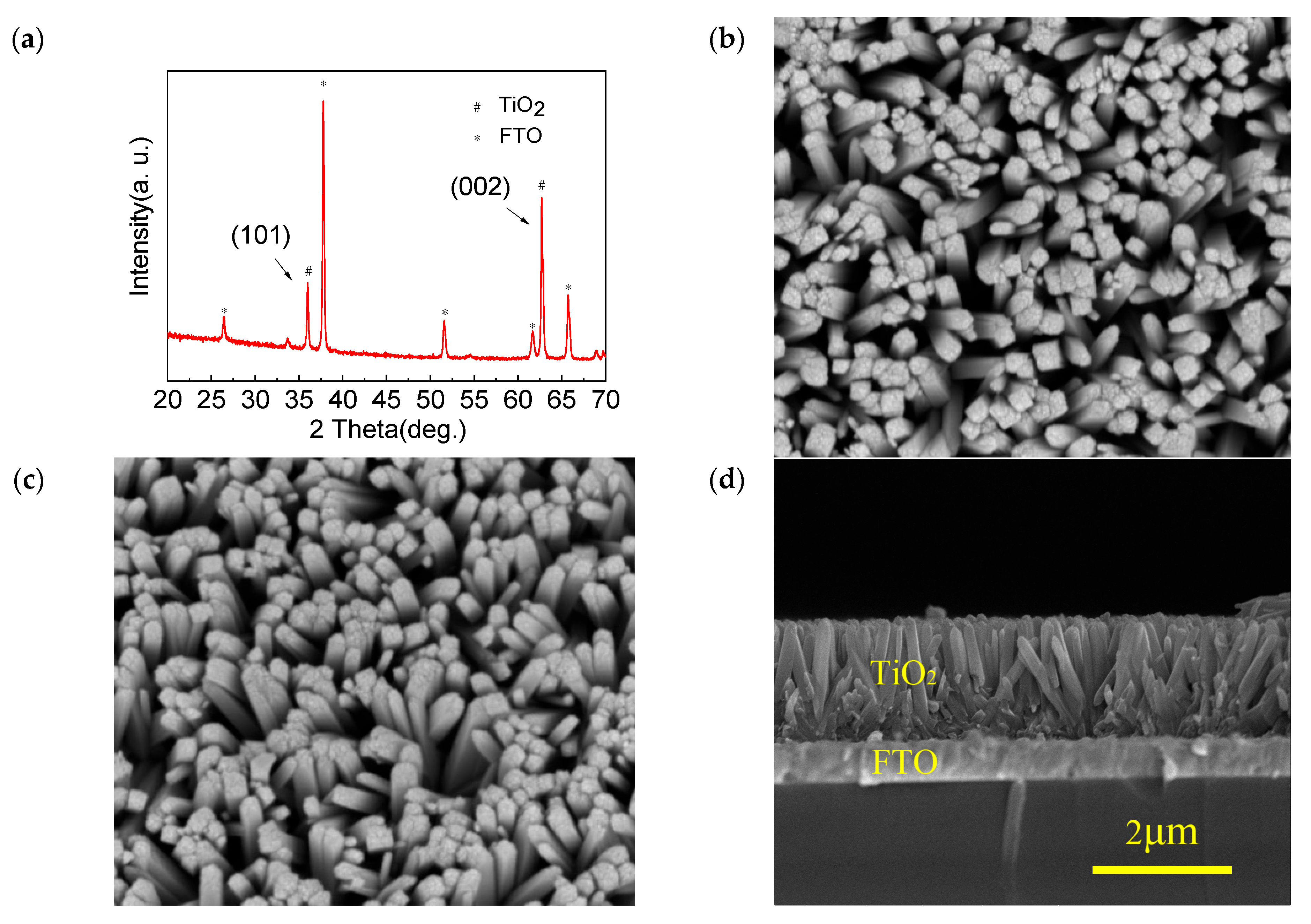
3.1. The Structure and Morphology of the TiO2 Nanowire Arrays

Figure 1a shows the XRD pattern of the TiO2 nanowire arrays. It is clear that there were only two sharp diffraction peaks, such as (101) and (002), observed at 36.20° and 62.84°, respectively, which can be assigned to the tetragonal rutile phase (JCPDS No. 88-1175) [17]. Moreover, the (002) diffraction peak was clearly enhanced compared with the (101) diffraction peak, while some diffraction peaks such as the (111), (211), and (110) crystal planes were absent, which suggests that the highly oriented TiO2 nanowire grew preferentially along the [001] orientation with the growth axis perpendicular to the FTO substrate. Figure 1b,c indicate the top-view and tilt-view FESEM images of the TiO2 nanowire arrays, respectively. It is observed that the FTO substrate was densely and uniformly covered by the vertically aligned TiO2 nanowire arrays with smooth edges and rough top surfaces. Figure 1d displays the cross-sectional FESEM image of the TiO2 nanowire arrays. It is clearly shown that the average height and diameter of the rutile TiO2 nanowire arrays were about 1.5 μm and 180 nm, respectively.

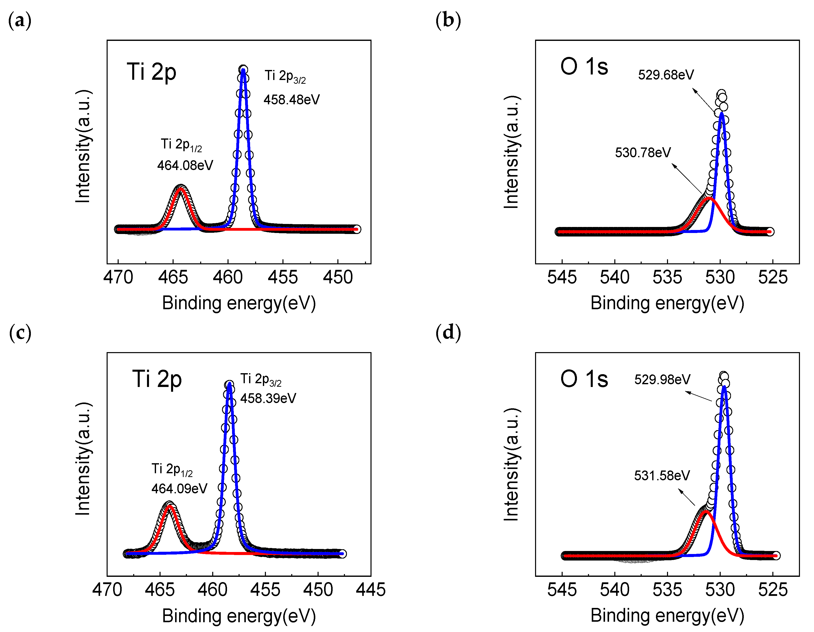
3.2. The Chemical Composition and Surface States of the TiO2 Nanowire Arrays

Figure 2 shows the XPS spectra of the Ti 2p and O 1 s in the rutile TiO2 nanowire arrays before and after the rapid nitrogen annealing treatment. As shown in Figure 2a, the Ti 2p3/2 and Ti 2p1/2 peaks around 458.48 eV and 464.08 eV can be observed. The spin-orbit splitting binding energy between Ti 2p3/2 and Ti 2p1/2 was approximately 5.6 eV, indicating the existence of Ti-O bonds in the rutile TiO2 nanowire arrays. Figure 2b reveals the XPS spectrum of O 1 s. It was found that the peak at the binding energy of 529.68 should be attributed to the lattice oxygen in the rutile TiO2 nanowire arrays, while the peak at the binding energy of 530.78 eV may be assigned to the oxygen vacancies, which suggests that the as-prepared rutile TiO2 nanowire arrays contained a considerable amount of oxygen vacancies, after the rapid nitrogen annealing treatment at 450 °C for 1 h, as shown in Figure 2c,d. It is obvious that the Ti 2p3/2 and Ti 2p1/2 peaks were found at 458.39 eV and 464.09 eV, respectively. In addition, the peak area of the 531.58 eV binding energy corresponding to the oxygen vacancies in Figure 2c was about 12.4% larger than that of the 530.78 eV binding energy in Figure 2a, which means that the nitrogen atoms entered the rutile TiO2 nanowire arrays and replaced the lattice oxygen atoms [32], resulting in an increase in the oxygen vacancies in the rutile TiO2 nanowire arrays.

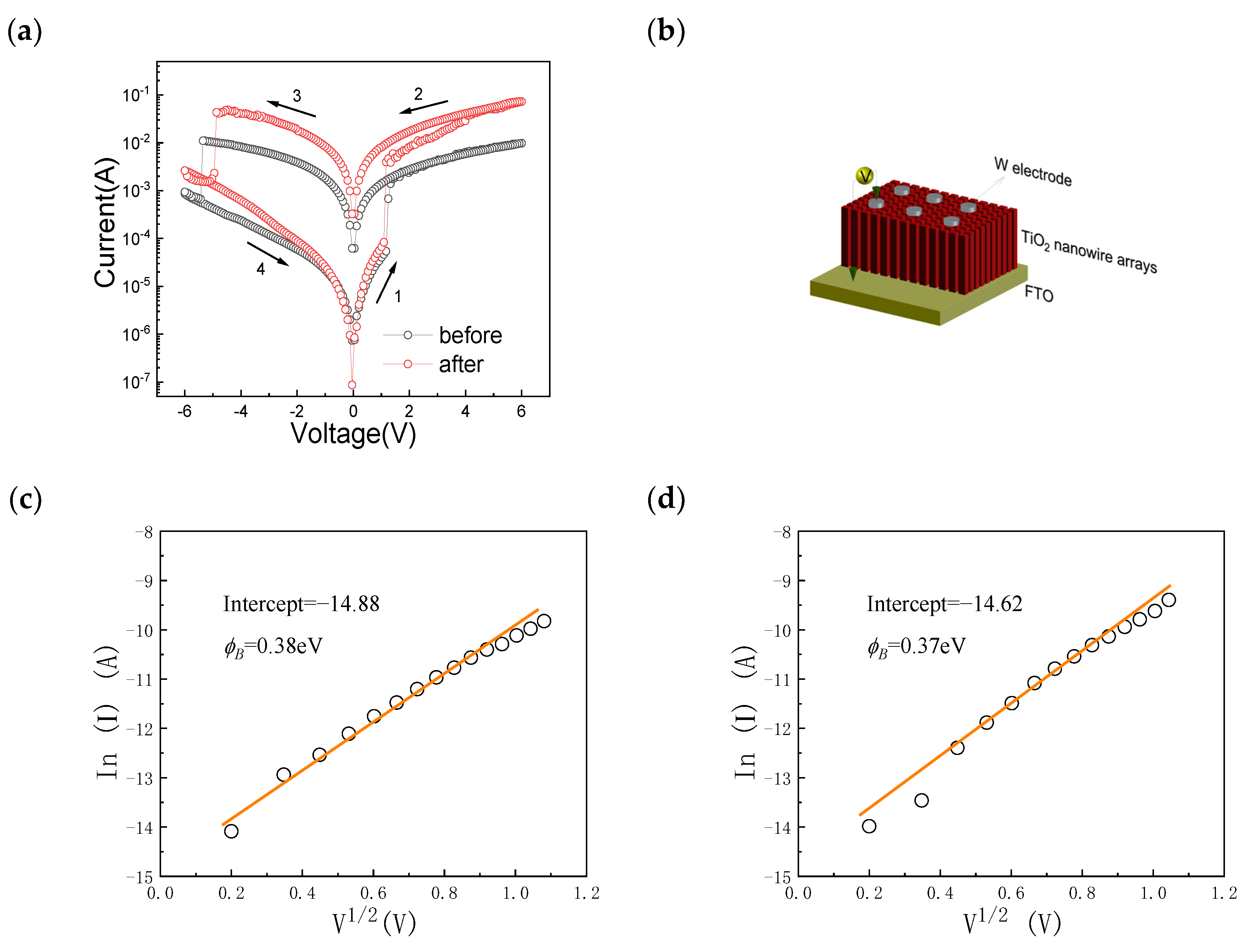
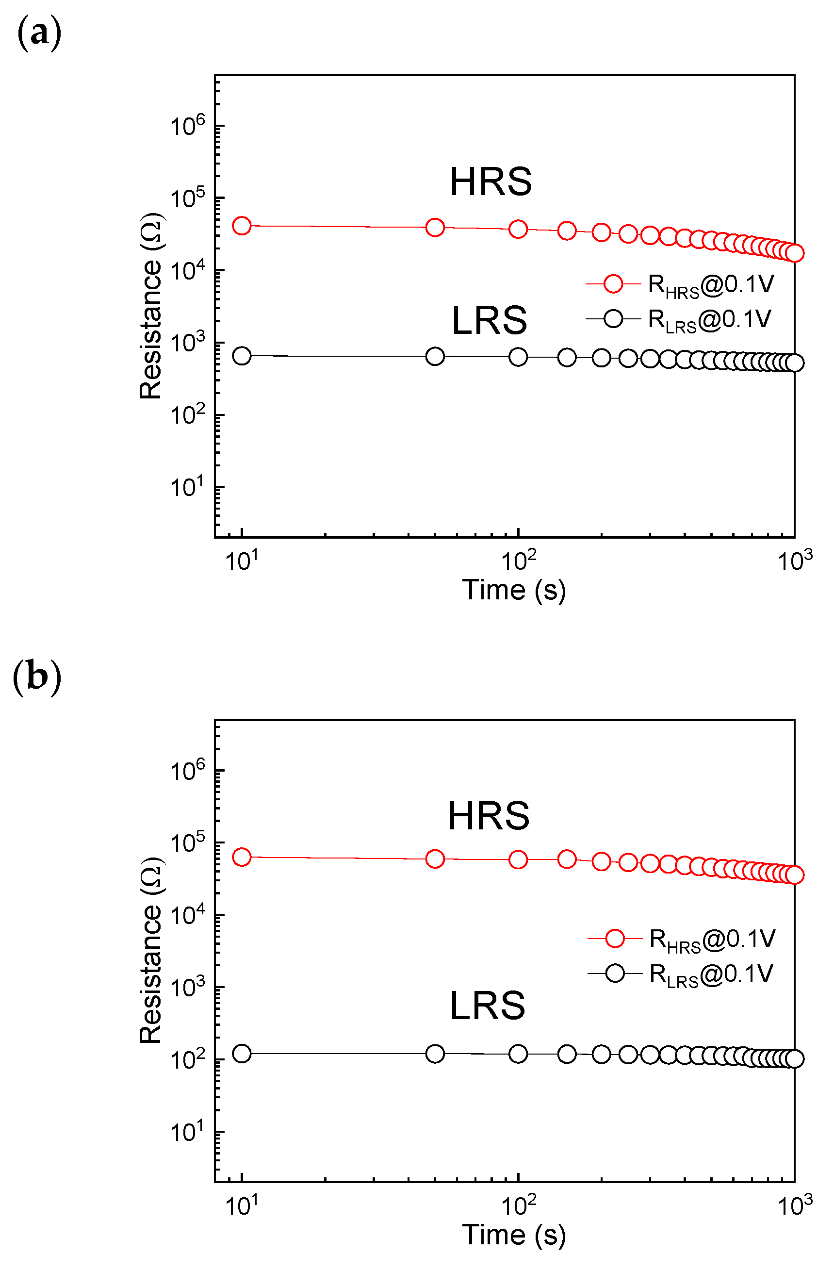
3.3. The Electrical Characteristics of the W/TiO2/FTO Memory Device

The typical current–voltage (I-V) measurements of the W/TiO2/FTO memory device were carried out to explain the resistive switching characteristics of the W/TiO2/FTO memory device before and after the rapid nitrogen annealing treatment, as shown in Figure 3a. The I-V curve plotted in semi-logarithmic scale was obtained by setting the applied voltage in a sequence of 0 V → +6 V → 0 V → −6 V → 0 V. Figure 3b displays the schematic diagram of the W/TiO2/FTO memory device, which is composed of the top W electrode, the TiO2 nanowire arrays, and the bottom FTO electrode. During the measurements, the voltages of the W/TiO2/FTO memory device were applied to the W electrode with the FTO electrode grounded. It is clear that the W/TiO2/FTO memory device showed nonvolatile bipolar resistive switching characteristics. The pristine resistance state of the W/TiO2/FTO memory device was the high resistance state (HRS). When the applied voltage increased from 0 V to +6 V, the W/TiO2/FTO memory device switched from the HRS to the LRS with a steep jump of current at +1.17 V (Vset), which indicated that the set process occurred. After that, the W/TiO2/FTO memory device maintained the LRS before the applied voltage reduced to −5.36 V (Vreset). Subsequently, the reset process occurred at Vreset, which induced a switch to the pristine HRS with a dramatic decrease in the current in the device, indicating the nonvolatile bipolar resistive switching behavior of the W/TiO2/FTO memory device. After the rapid nitrogen annealing treatment, the Vset and Vreset reduced to 1.09 V and −4.87 V, respectively, and the operation current in the LRS for the device was higher than that of the device before the rapid nitrogen annealing treatment. Figure 3c,d show the I-V curves plotted in I n I ~ V 1 / 2 scale before and after the rapid nitrogen annealing treatment, respectively. It is observed that the W/TiO2 Schottky barrier heights of the W/TiO2/FTO memory device were about 0.38 eV and 0.37 eV before and after the nitrogen annealing, respectively. Thus, the change in the W/TiO2 Schottky barrier modified by the oxygen vacancies is suggested to be responsible for the resistive switching characteristics of the W/TiO2/FTO memory device.
The current–voltage characteristics of the Schottky emission are described as [29]:
J A T 2 exp [ q B q V / 4 π ε k T ] ,
where J is the current density, T is the absolute temperature, V is the electric field, A is the Richardson constant, k is the Boltzmann’s constant, ε is the dielectric constant, q is the electric charge, and B is the Schottky barrier height. According to the above fitting results, the conduction behaviors of the W/TiO2/FTO memory device are attributed to the Schottky emission in the high resistance state, and the change in the W/TiO2 Schottky barrier depletion layer thickness and barrier height modified by the oxygen vacancies at the W/TiO2 interface is suggested to be responsible for the resistive switching characteristics of the W/TiO2/FTO memory device. For the W/TiO2/FTO memory device, the work function of tungsten was 4.6 eV, and the work function of the intrinsic rutile TiO2 was about 4.2 eV. Therefore, when the W/TiO2 Schottky junction was formed, electrons from the Fermi level of the rutile TiO2 migrated toward the W until the Fermi levels on both sides equalized, and the height of the W/TiO2 Schottky junction depletion barrier was about 0.4 eV. As shown in Figure 3, the Schottky barrier heights of the W/TiO2 Schottky barrier depletion layer were about 0.38 eV and 0.37 eV before and after the rapid nitrogen annealing treatment, respectively, which were smaller than that of the intrinsic rutile TiO2 because of the existence of oxygen vacancies in the rutile TiO2.
In order to evaluate the effect of the nitrogen annealing on the resistive switching characteristics of the W/TiO2/FTO memory device, Figure 4a,b exhibit the retention tests of the device at the reading voltage of 0.1 V before and after the rapid nitrogen annealing treatment, respectively. As shown in Figure 4a, the W/TiO2/FTO memory device displayed the nonvolatile resistive switching characteristics with a high resistance ratio (RHRS/RLRS) of about two orders of magnitude, which could be stably preserved for over 103 s without obvious degradation. Figure 4b indicates the retention tests of the device at the reading voltage of 0.1 V after the rapid nitrogen annealing treatment, it is appreciable that the RHRS/RLRS of the W/TiO2/FTO memory device increased from about two orders of magnitude to three orders of magnitude after the rapid nitrogen annealing treatment. In comparison with the previous reports about TiO2 memory devices as summarized in Table 1 [16,17,18,19,21,22,23,24,25,26,27,28,29,31], the W/TiO2/FTO memory device in this work has a relatively lower Vset and the highest resistance ratio of about three orders of magnitude, which demonstrates the outstanding potential of the W/TiO2/FTO memory device for the future nonvolatile memory applications.

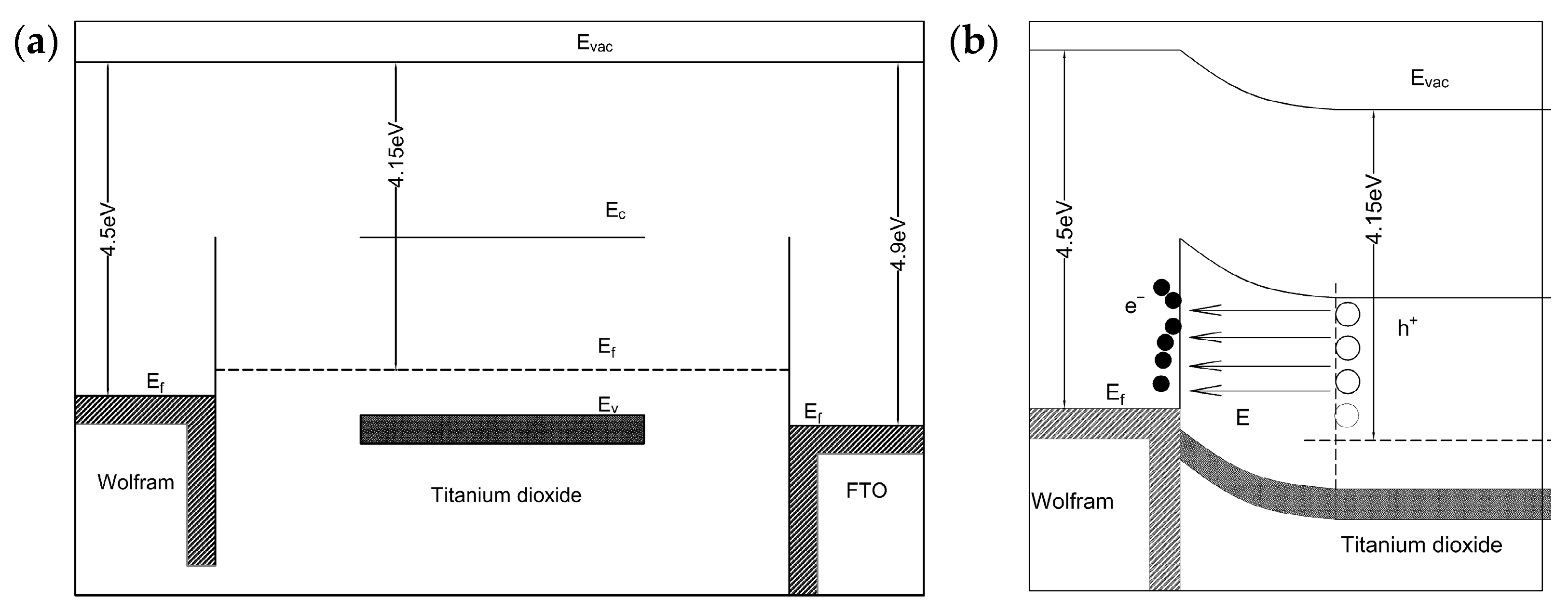
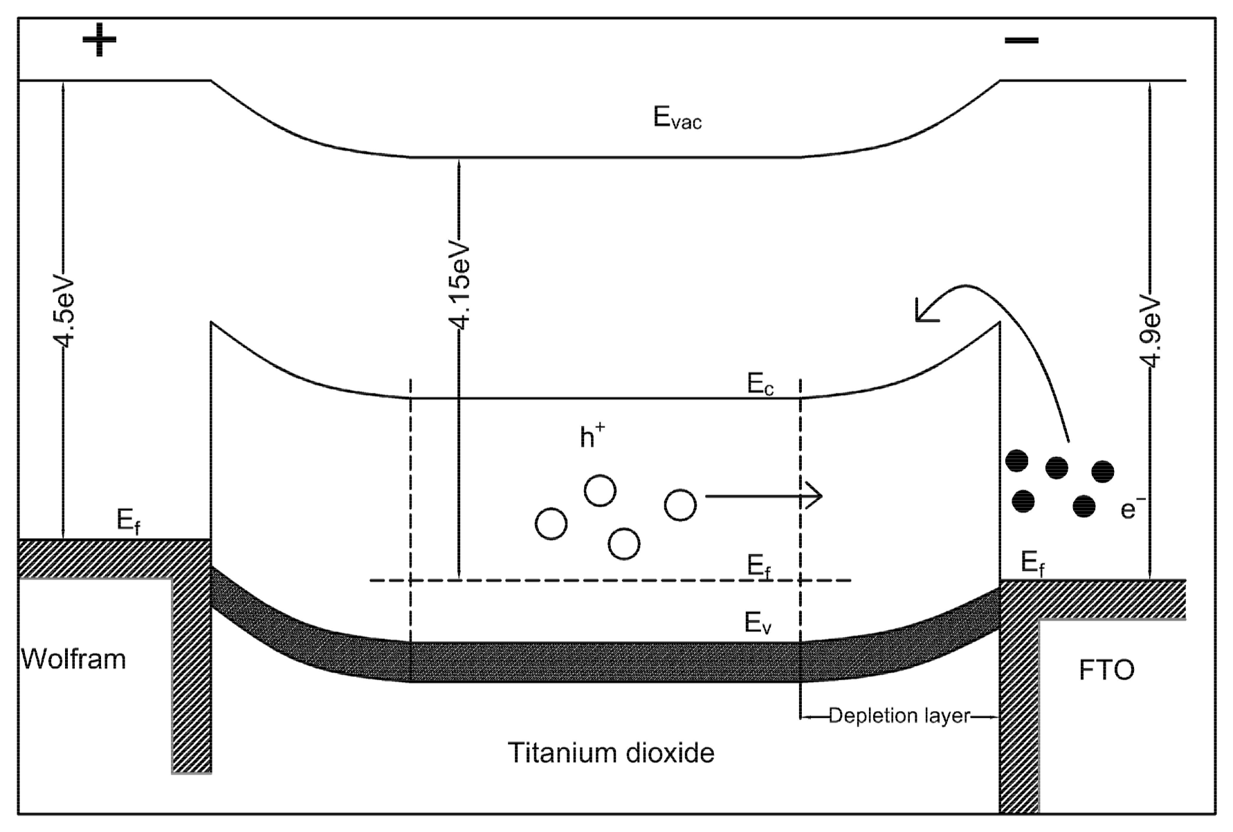
3.4. The Resistive Switching Mechanism of the W/TiO2/FTO Memory Device

To further illustrate the resistive switching mechanism of the W/TiO2/FTO memory device, Figure 5 shows the schematic diagram of the relative band positions of the W, TiO2, and FTO before and after the formation of the W/TiO2 Schottky interface. It was found that the work function of W was about 4.6 eV, which was higher than that of TiO2 (4.2 eV). Therefore, the electrons migrated from the Fermi level of the TiO2 to the W electrode until the Fermi levels on both sides equalized when the W/TiO2 Schottky interface was formed, which pushed the conduction band of the W electrode to a relatively higher energy level with respect to the conduction band position of the TiO2. Thus, the change in the W/TiO2 Schottky barrier depletion layer thickness and barrier height modified by the oxygen vacancies at the W/TiO2 interface is suggested to be responsible for the resistive switching characteristics of the W/TiO2/FTO memory device. During the set process as displayed in Figure 6, when the positive voltage was applied to the W/TiO2/FTO memory device, the electrons were injected from the bottom FTO electrode and captured by the oxygen vacancies in the W/TiO2 Schottky barrier depletion layer, resulting in lowering the W/TiO2 Schottky barrier height and barrier thickness. Once the W/TiO2 Schottky barrier became low and thin enough, large amounts of electrons from the TiO2 side crossed the W/TiO2 Schottky barrier, thus switching the W/TiO2/FTO memory device from the HRS to the LRS with an abrupt increase in the current at Vset. Subsequently, the device maintained the LRS until a large enough negative voltage Vreset was applied, indicating the nonvolatile resistive switching behavior of the W/TiO2/FTO memory device. During the reset process, when the negative voltage was applied to the W/TiO2/FTO memory device, the electrons injected from the top W electrode were retarded by the W/TiO2 Schottky barrier, which induced a large electric field to cross the W/TiO2 Schottky barrier depletion layer. Thus, the electrons captured by the oxygen vacancies were activated and emitted from the W/TiO2 Schottky barrier depletion layer to the bottom FTO electrode, which induced a recovery to the initial state of the W/TiO2 Schottky barrier, and the device switched back from the LRS to the HRS with a drastic drop in the current at Vreset. This work suggests that the W/TiO2/FTO memory device may be a potential candidate for future nonvolatile memory applications.
After the rapid nitrogen annealing treatment, N atoms entered the surface of the TiO2 nanowire arrays and replaced the O atoms, which resulted in the increase in oxygen vacancies at the W/TiO2 Schottky barrier. It is worth noting that the increase in the oxygen vacancies at the W/TiO2 Schottky interface led to reducing the depletion layer thickness and lowering the barrier height of the W/TiO2 Schottky barrier. Thus, a lower Schottky barrier height of 0.37 eV and smaller set voltage of 1.09 V (Vset), as well as a higher resistance ratio of about three orders of magnitude, were observed after the rapid nitrogen annealing treatment, as shown in Figure 3.

4. Conclusions

In this paper, the rutile TiO2 nanowire-based W/TiO2/FTO memory device with a high resistance ratio of about three orders of magnitude was successfully obtained by the rapid N2 annealing treatment. The as-prepared W/TiO2/FTO memory device exhibits nonvolatile bipolar resistive switching behavior. Furthermore, the RHRS/RLRS of the W/TiO2/FTO memory device was obviously increased from about two orders of magnitude to three orders of magnitude after the rapid N2 annealing treatment. The conduction behaviors of the W/TiO2/FTO memory device are attributed to the Ohmic conduction mechanism and the Schottky emission in the low resistance state and the high resistance state, respectively. In addition, the change in the W/TiO2 Schottky barrier depletion layer thickness and barrier height modified by the oxygen vacancies at the W/TiO2 interface has been suggested to be responsible for the nonvolatile resistive switching phenomena of the W/TiO2/FTO memory device. This work demonstrates that the rutile TiO2 nanowire-based W/TiO2/FTO memory device may be an outstanding candidate for application in the future nonvolatile memory devices.

Author Contributions

Z.Y. guided the experimental method and the paper writing. X.H. completed the experiment and wrote the paper. J.X., C.C. and X.Q. verified the repeatability of the experiment. B.L., Z.S. and T.S. defined the review scope, context, and purpose of the study. All authors have read and agreed to the published version of the manuscript.

Funding

This project was supported by the National Natural Science Foundation of China (Grant No. 61805053), the Guangxi Science and Technology Project (Grant Nos. AD19110038, AD19110003), the Scientific Research Foundation of Guangxi Education Department (Grant No. 2019KY03927), the Scientific Research Foundation of Guangxi University of Science and Technology (Grant No. 19Z07), and the Innovation Project of Guangxi Graduate Education (Grant No. YCSW2021135).

Institutional Review Board Statement

Not applicable.

Informed Consent Statement

Not applicable.

Data Availability Statement

The review was based on publicly available academic literature databases.

Acknowledgments

This work was supported by Guangxi University of Science and Technology.

Conflicts of Interest

The authors declare no conflict of interest.

References

  1. Chua, L. Memristor-The missing circuit element. IEEE Trans. Circuit Theory 1971, 18, 507–519. [Google Scholar] [CrossRef]
  2. Strukov, D.B.; Snider, G.S.; Stewart, D.R.; Williams, R. The missing memristor found. Nature 2008, 453, 80–83. [Google Scholar] [CrossRef] [PubMed]
  3. Xla, B.; Zza, B.; Dcwi, C. Memristor-based LSTM network with in situ training and its applications. Neural Netw. 2020, 131, 300–311. [Google Scholar]
  4. Yu, F.; Kong, X.; Mokbel AA, M.; Yao, W.; Cai, S. Complex Dynamics, Hardware Implementation and Image Encryption Application of Multiscroll Memeristive Hopfield Neural Network with a Novel Local Active Memeristor. IEEE Trans. Circuits Syst. II Express Briefs 2023, 70, 326–330. [Google Scholar] [CrossRef]
  5. Rehman, S.; Khan, M.F.; Rahmani, M.K.; Kim, H.; Patil, H.; Khan, S.A.; Kang, M.H.; Kim, D.-k. Neuro-transistor based on uv-treated charge trapping in MoTe2 for artificial synaptic features. Nanomaterials 2020, 10, 2326. [Google Scholar] [CrossRef]
  6. Yang, S. Dynamical analysis and image encryption application of a novel memristive hyperchaotic system. Opt. Laser Technol. 2021, 133, 106553. [Google Scholar] [CrossRef]
  7. Sahin, M.E.; Taskiran, Z.C.; Guler, H.; Hamamci, S.E. Simulation and implementation of memristive chaotic system and its application for communication systems. Sens. Actuators A Phys. 2019, 290, 107–118. [Google Scholar] [CrossRef]
  8. Sun, J.; Han, J.; Wang, Y.; Liu, P. Memristor-based neural network circuit of emotion congruent memory with mental fatigue and emotion inhibition. IEEE Trans. Biomed. Circuits Syst. 2021, 15, 606–616. [Google Scholar] [CrossRef]
  9. Yang, T.; Wang, H.; Zhang, B.; Yan, X. Enhanced memory characteristics of charge trapping memory by employing graphene oxide quantum dots. Appl. Phys. Lett. 2020, 116, 103501. [Google Scholar] [CrossRef]
  10. Sun, T.; Tu, J.; Zhou, Z.; Sun, R.; Zhang, X.; Li, H.; Xu, Z.; Peng, Y.; Liu, X.; Wangyang, P.; et al. Resistive switching of self-assembly stacked h-BN polycrystal film. Cell Rep. Phys. Sci. 2022, 3, 100939. [Google Scholar] [CrossRef]
  11. Sun, T.; Liu, Y.; Tu, J.; Zhou, Z.; Cao, L.; Liu, X.; Li, H.; Li, Q.; Fu, T.; Zhang, F.; et al. Wafer-scale high anti-reflective nano/micro hybrid interface structures via aluminum grain dependent self-organization. Mater. Des. 2020, 194, 108960. [Google Scholar] [CrossRef]
  12. Li, H.; Cao, L.; Fu, T.; Li, Q.; Zhang, F.; Xiao, G.; Chen, Y.; Liu, X.; Zhao, W.; Yu, Z.; et al. Morphology-dependent high antireflective surfaces via anodic aluminum oxide nanostructures. Appl. Surf. Sci. 2019, 496, 143697. [Google Scholar] [CrossRef]
  13. Yang, J.J.; Pickett, M.D.; Li, X.; Ohlberg, D.A.; Stewart, D.R.; Williams, R.S. Memristive switching mechanism for metal/oxide/metal nanodevices. Nat. Nanotechnol. 2008, 3, 429–433. [Google Scholar] [CrossRef] [PubMed]
  14. Zhong, P.; Ma, X.; Chen, X.; Zhong, R.; Liu, X.; Ma, D.; Zhang, M.; Li, Z. Morphology-controllable polycrystalline TiO2 nanorod arrays for efficient charge collection in dye-sensitized solar cells. Nano Energy 2015, 16, 99–111. [Google Scholar] [CrossRef]
  15. Perillo, P.M.; Rodriguez, D.F. A room temperature chloroform sensor using TiO2 nanotubes. Sens. Actuators B Chem. 2014, 193, 263–266. [Google Scholar] [CrossRef]
  16. Xiao, M.; Musselman, K.P.; Duley, W.W.; Zhou, Y.N. Reliable and Low-Power Multilevel Resistive Switching in TiO2 Nanorod Arrays Structured with a TiOx Seed Layer. ACS Appl. Mater. Interfaces 2017, 9, 4808–4817. [Google Scholar] [CrossRef]
  17. Zhang, F.; Gan, X.; Li, X.; Wu, L.; Gao, X.; Zheng, R.; He, Y.; Liu, X.; Yang, R. Realization of Rectifying and Resistive Switching Behaviors of TiO2 Nanorod Arrays for Nonvolatile Memory. Electrochem. Solid-State Lett. 2011, 14, H422–H425. [Google Scholar] [CrossRef]
  18. Yu, Y.; Wang, C.; Jiang, C.; Wang, L.; Wang, Z.; Du, Z.; Sun, J.; Abrahams, I.; Huang, X. Nitrogen-doped titanium dioxide nanorod array memristors with synaptic features and tunable memory lifetime for neuromorphic computing. J. Alloys Compd. 2021, 868, 159194. [Google Scholar] [CrossRef]
  19. Sun, B.; Li, Q.L.; Zhao, W.X.; Li, H.W.; Wei, L.J.; Chen, P. White-light-controlled resistance switching in TiO2/α-Fe2O3 composite nanorods array. J. Nanopart. Res. 2014, 16, 2389. [Google Scholar] [CrossRef]
  20. Hu, S.; Yue, J.; Jiang, C.; Tang, X.; Huang, X.; Du, Z.; Wang, C. Resistive switching behavior and mechanism in flexible TiO2@Cf memristor crossbars. Ceram. Int. 2019, 45, 10182–10186. [Google Scholar] [CrossRef]
  21. Wang, H.J.; Zhu, Y.Y.; Fu, D.J. Coexistence of bipolar and unipolar resistive switching characteristics of thin TiO2 film grown on Cu foil substrate for flexible nonvolatile memory device. J. Alloys Compd. 2017, 695, 2669–2671. [Google Scholar] [CrossRef]
  22. Park, J.; Biju, K.P.; Jung, S.; Lee, W.; Lee, J.; Kim, S.; Park, S.; Shin, J.; Hwang, H. Multibit Operation of TiOx-Based ReRAM by Schottky Barrier Height Engineering. IEEE Electron Device Lett. 2011, 32, 476–478. [Google Scholar] [CrossRef]
  23. Chen, J.; Wu, Y.; Zhu, K.; Sun, F.; Guo, C.; Wu, X.; Cheng, G.; Zheng, R. Core-shell copper nanowire-TiO2 nanotube arrays with excellent bipolar resistive switching properties. Electrochim. Acta 2019, 316, 133–142. [Google Scholar] [CrossRef]
  24. Yu, Y.; Yang, F.; Mao, S.; Zhu, S.; Jia, Y.; Yuan, L.; Salmen, M.; Sun, B. Effect of anodic oxidation time on resistive switching memory behavior based on amorphous TiO2 thin films device. Chem. Phys. Lett. 2018, 706, 477–482. [Google Scholar] [CrossRef]
  25. Kim, S.E.; Lee, J.G.; Ling, L.; Liu, S.E.; Lim, H.K.; Sangwan, V.K.; Hersam, M.C.; Lee, H.-B. Sodium-Doped Titania Self-Rectifying Memristors for Crossbar Array Neuromorphic Architectures. Adv. Mater. 2022, 34, 2106913. [Google Scholar] [CrossRef]
  26. Fu, L.P.; Song, X.Q.; Gao, X.P.; Wu, Z.W.; Chen, S.K.; Li, Y.T. TiOx-based self-rectifying memory device for crossbar WORM memory array applications. Chin. Phys. B 2021, 30, 016103. [Google Scholar] [CrossRef]
  27. Chu, D.W.; Younis, A.; Li, S.A. Direct growth of TiO2 nanotubes on transparent substrates and their resistive switching characteristics. J. Phys. D Appl. Phys. 2012, 45, 355306. [Google Scholar] [CrossRef]
  28. Bogle, K.A.; Bachhav, M.N.; Deo, M.S.; Valanoor, N.; Ogale, S.B. Enhanced nonvolatile resistive switching in dilutely cobalt doped TiO2. Appl. Phys. Lett. 2009, 95, 203502. [Google Scholar] [CrossRef]
  29. Zou, L.; Hu, W.; Xie, W.; Bao, D. Uniform resistive switching properties of fully transparent TiO2-based memory devices. J. Alloys Compd. 2017, 693, 1180–1184. [Google Scholar] [CrossRef]
  30. Manning, H.G.; Biswas, S.; Holmes, J.D.; Boland, J.J. Nonpolar Resistive Switching in Ag@TiO2 Core-Shell Nanowires. ACS Appl. Mater. Interfaces 2017, 9, 38959–38966. [Google Scholar] [CrossRef]
  31. Park, J.; Park, E.; Kim, S.; Yu, H.Y. Nitrogen-Induced enhancement of synaptic weight reliability in titanium oxide-based resistive artificial synapse and demonstration of the reliability effect on the neuromorphic system. ACS Appl. Mater. Interfaces 2019, 11, 32178–32185. [Google Scholar] [CrossRef] [PubMed]
  32. Asahi, R.; Morikawa, T.; Ohwaki, T.; Aoki, K.; Taga, Y. Visible-Light Photocatalysis in Nitrogen-Doped Titanium Oxides. Science 2001, 293, 269–271. [Google Scholar] [CrossRef] [PubMed]
Figure 1. (a) XRD pattern of the TiO2 nanowire arrays. (b) Top-view FESEM image of the TiO2 nanowire arrays. (c) Tilt-view FESEM image of the TiO2 nanowire arrays. (d) Cross-sectional FESEM image of the TiO2 nanowire arrays.
Sensors 23 03480 g001
Figure 2. (a) Ti 2p and (b) O 1 s high resolution XPS spectra of the TiO2 nanowire arrays. (c) Ti 2p and (d) O 1 s high resolution XPS spectra of the TiO2 nanowire arrays after the rapid nitrogen annealing treatment.
Sensors 23 03480 g002
Figure 3. (a) The semi-logarithmic I-V curves of the W/TiO2/FTO memory device before and after annealing. (b) Schematic diagram of the W/TiO2/FTO memory device. The I-V curves plotted in I n I ~ V 1 / 2 scale (c) before and (d) after the rapid nitrogen annealing treatment.
Sensors 23 03480 g003
Figure 4. Retention tests of the device at the reading voltage of 0.1 V (a) before and (b) after the rapid nitrogen annealing treatment.
Sensors 23 03480 g004
Figure 5. Schematic diagram of the relative band positions of the W, TiO2, and FTO (a) before and (b) after the formation of the W/TiO2 Schottky interface.
Sensors 23 03480 g005
Figure 6. Schematic of the resistive switching mechanism of the W/TiO2/FTO memory device.
Sensors 23 03480 g006
Table 1. Summary of the performance parameters for the TiO2 based memory devices.
Device StructureVset/Vreset (V)Preparation MethodRHRS/RLRS RatioRetention (s)Reference
Al/TiO2/TiOx/FTO~+4/~−4Hydrothermal>203 × 104[16]
Pt/TiO2 NRAs/FTO+1.5/−1.5Hydrothermal~103 × 105[17]
Al/N-TiO2 NARs/FTO~−3/~+3Hydrothermal>16-[18]
Ag/[TiO2/α-Fe2O3]/FTO~+4/~−4Hydrothermal~10103[19]
Ni/TiO2/Cu−0.5/+0.35Magnetron sputtering~101.5 × 10³[21]
Ir/TiOx/TiN~−1/~+1.5Magnetron sputtering~10104[22]
Au/Cu NWs/TiO2 NTAs/Ti+0.6/−0.9Electrochemical anodization>40104[23]
Ag/TiO2/Ti+0.59/−0.58Anodic oxidation~27-[24]
Pt/Na-doped TiO2/Pt~+2/~−2Atomic layer deposition~30105[25]
Pt/TiOx/W−5/+2Atomic layer deposition>10104[26]
Au/TiO2 nanotube/FTO+2.5/−1.3Electrochemical deposition~9-[27]
Cu/TiO2−δ/Pt+1.5/−1.5Pulsed laser deposition105 × 103[28]
ITO/TiO2/FTO~+1/~−0.8Chemical solution deposition>10104[29]
Ti/TiOx/Pt~+1.5/~−1.4Magnetron sputtering~10-[31]
W/TiO2/FTO+1.09/−4.87Hydrothermal~103103This work
Disclaimer/Publisher’s Note: The statements, opinions and data contained in all publications are solely those of the individual author(s) and contributor(s) and not of MDPI and/or the editor(s). MDPI and/or the editor(s) disclaim responsibility for any injury to people or property resulting from any ideas, methods, instructions or products referred to in the content.

