
Fabrication of Vertical MEMS Actuator with Hollow Square Electrode for SPR Sensing Applications

Abstract
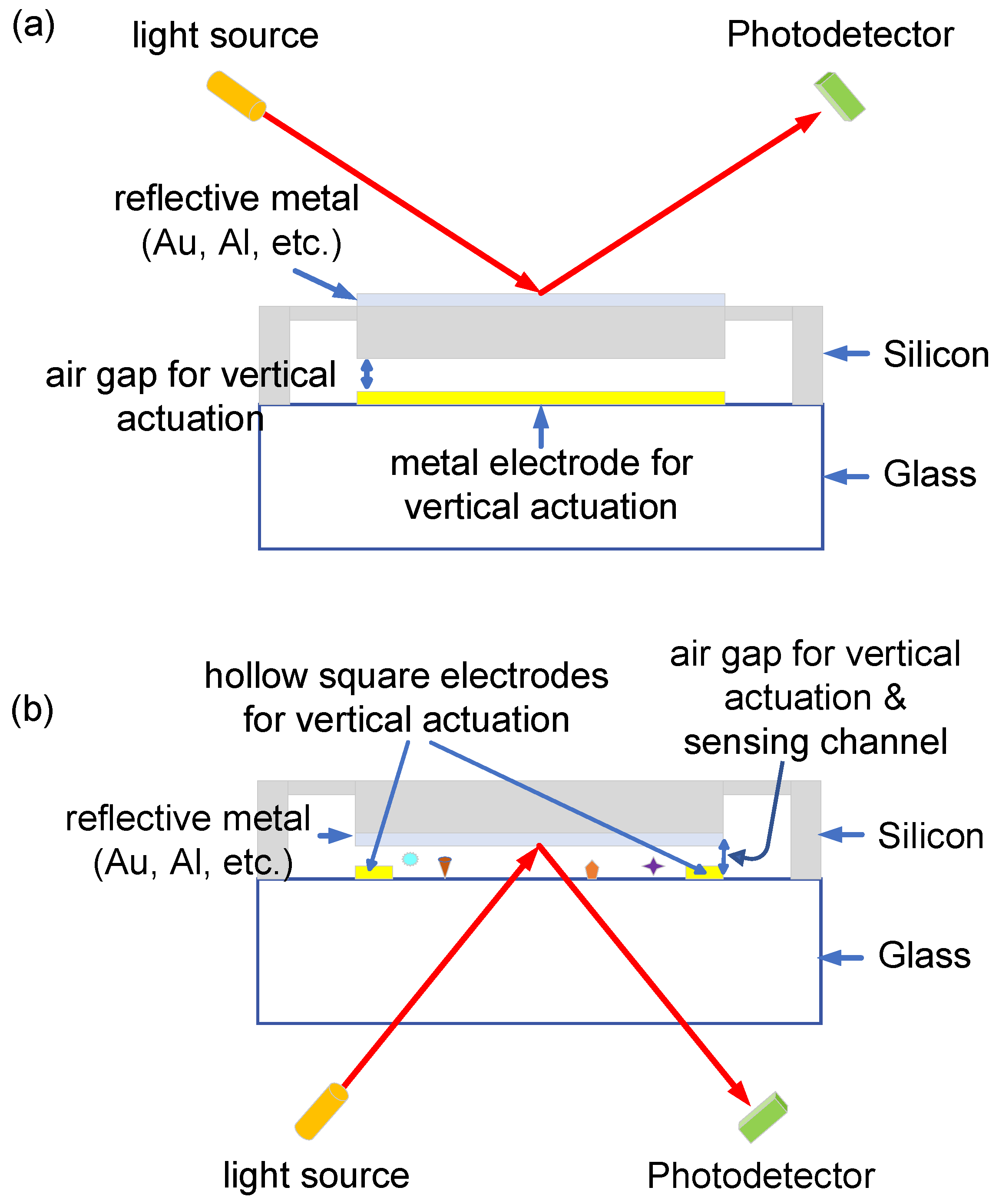
:1. Introduction
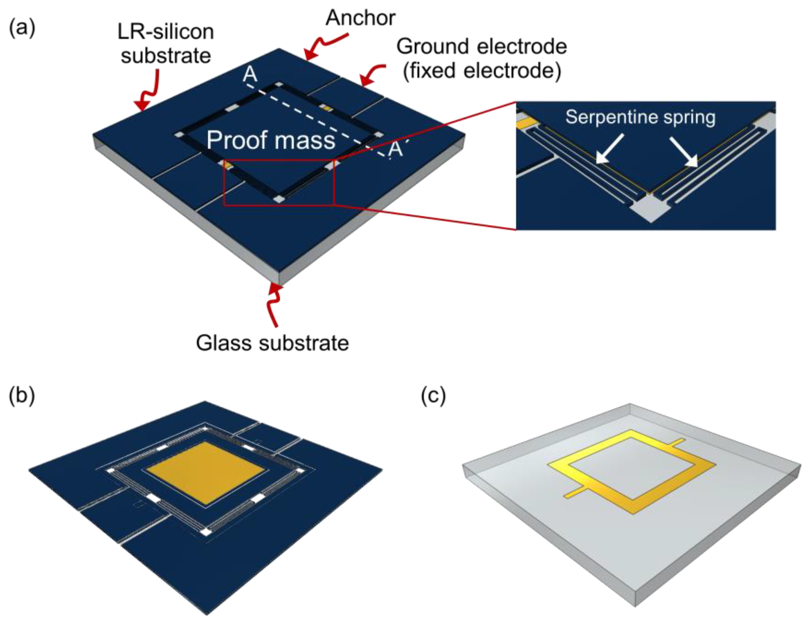
2. Design and Fabrication
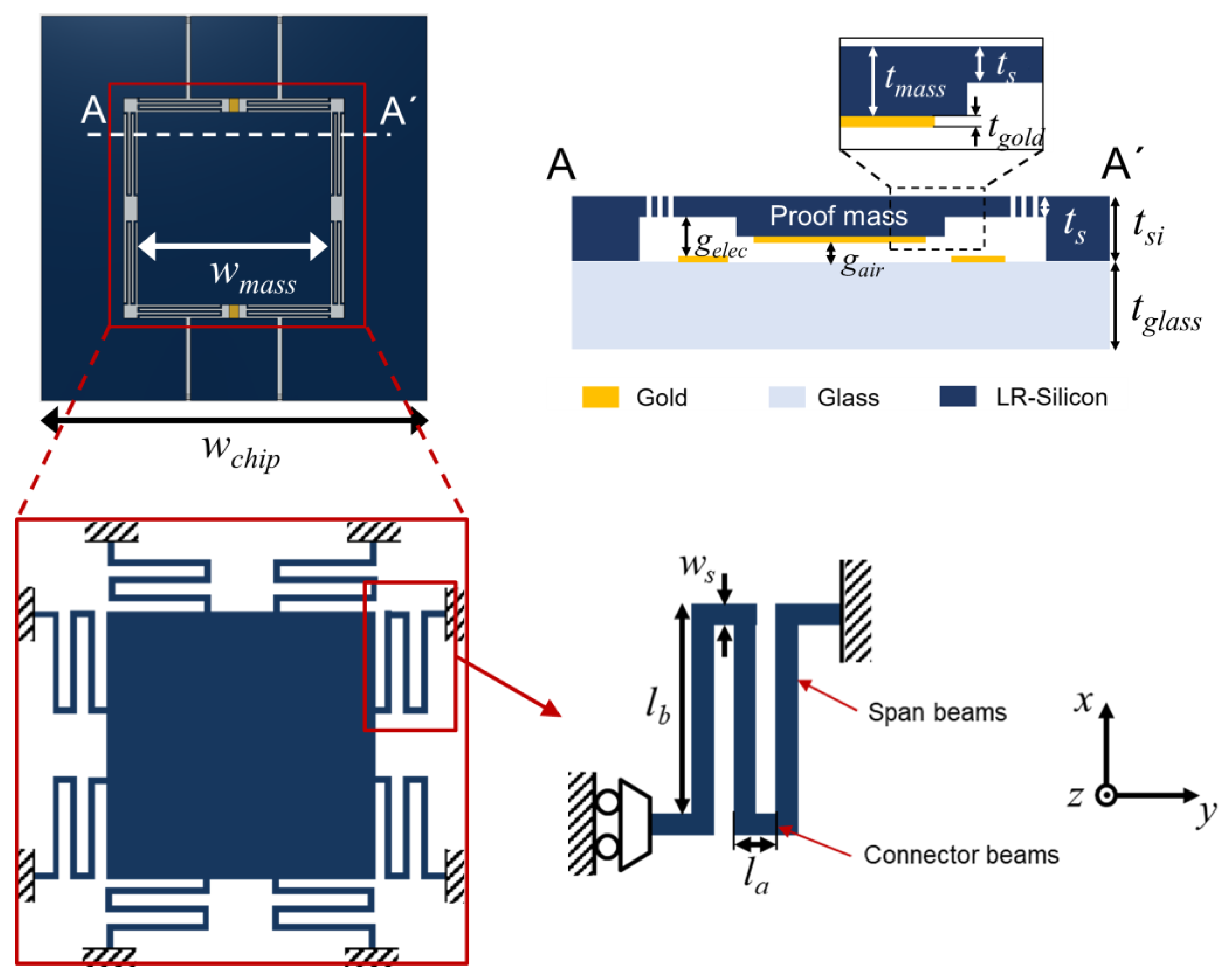
2.1. Design of the Vertical MEMS Actuator
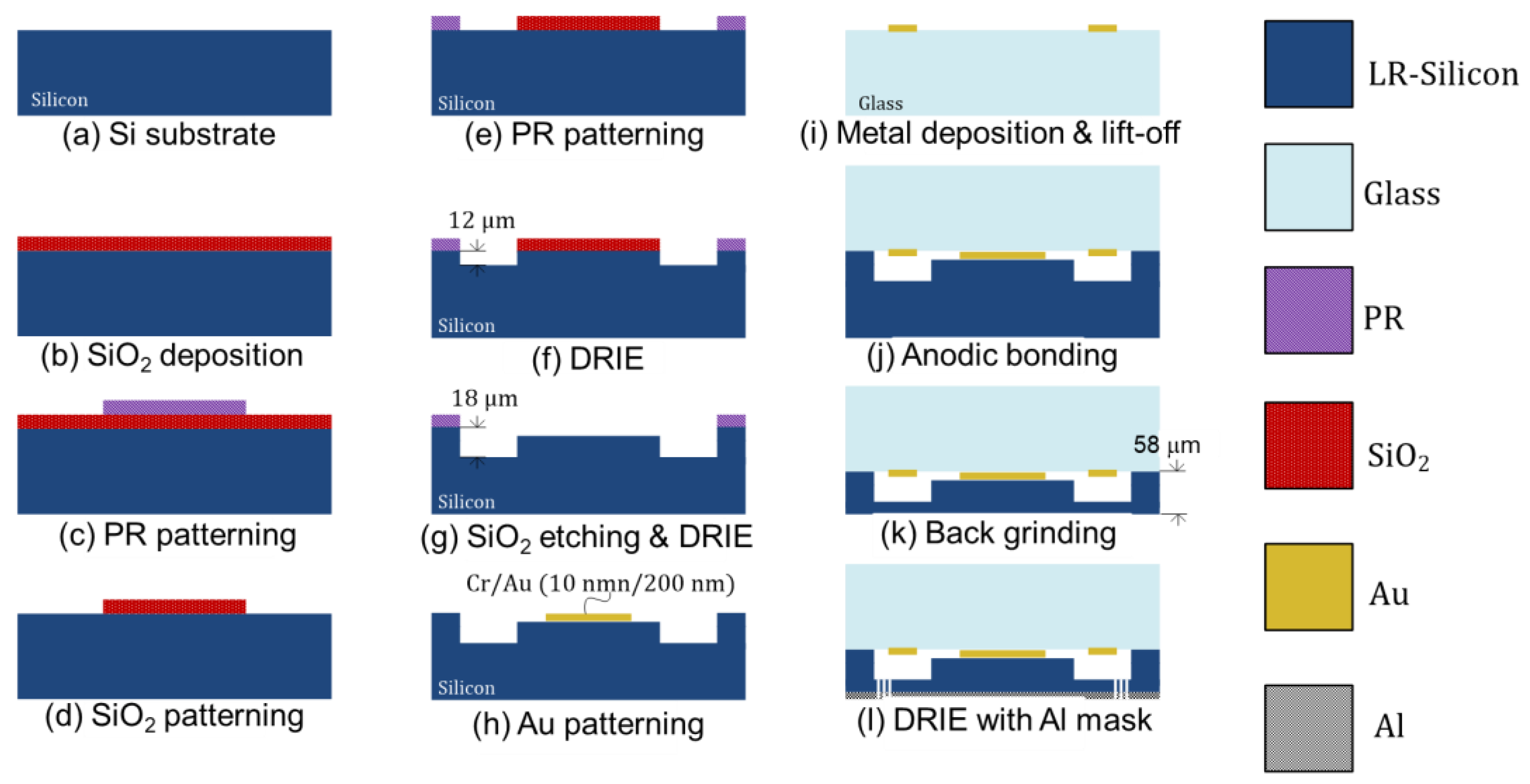
2.2. Fabrication of the Vertical MEMS Actuator
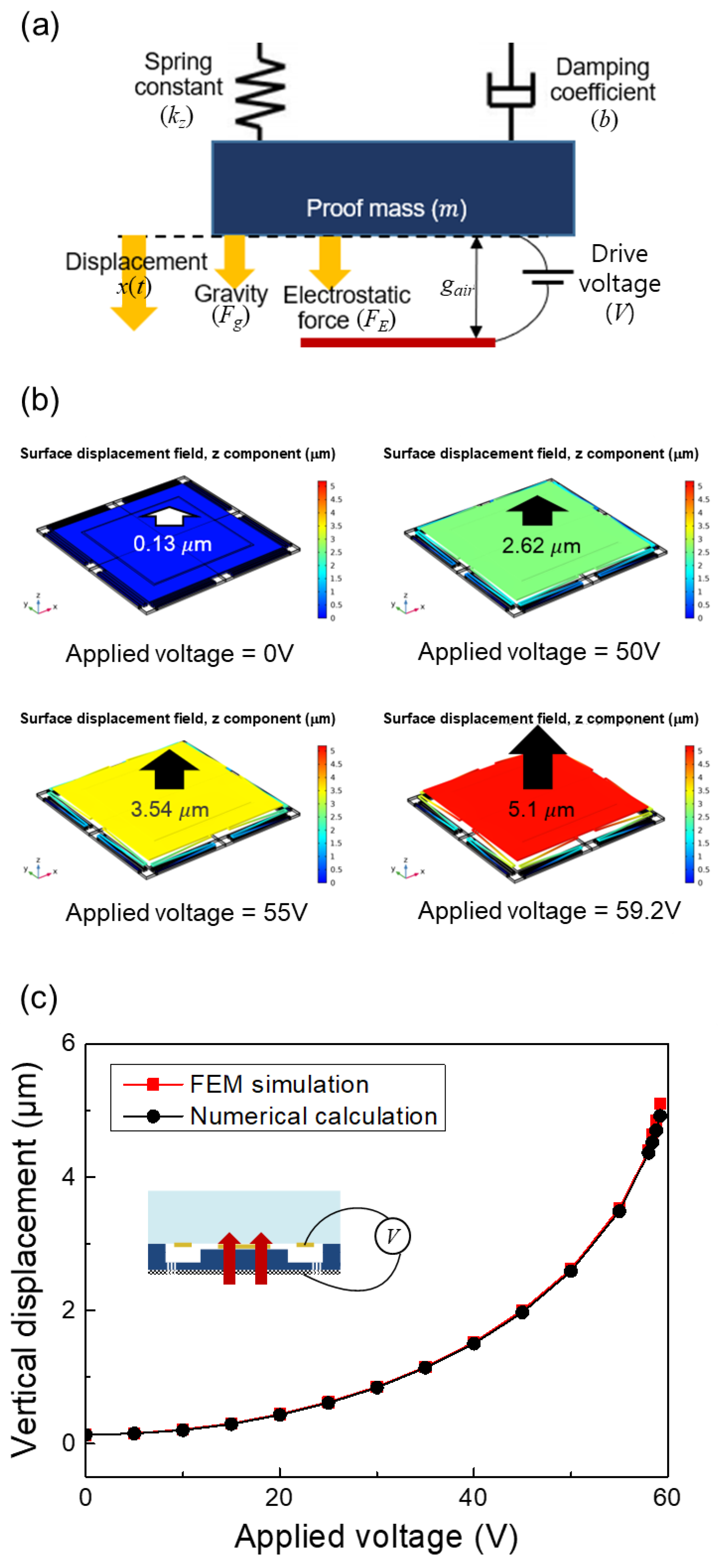
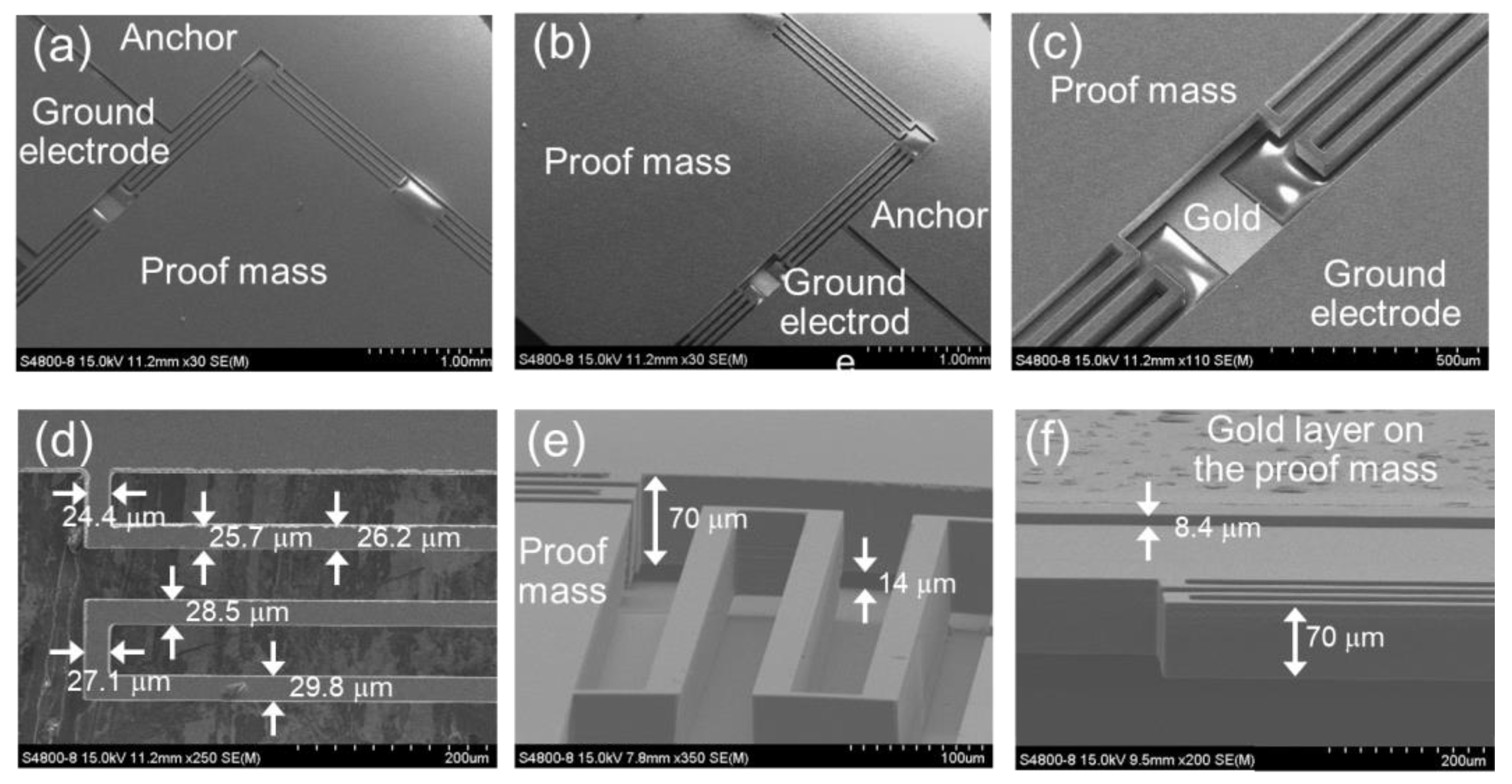
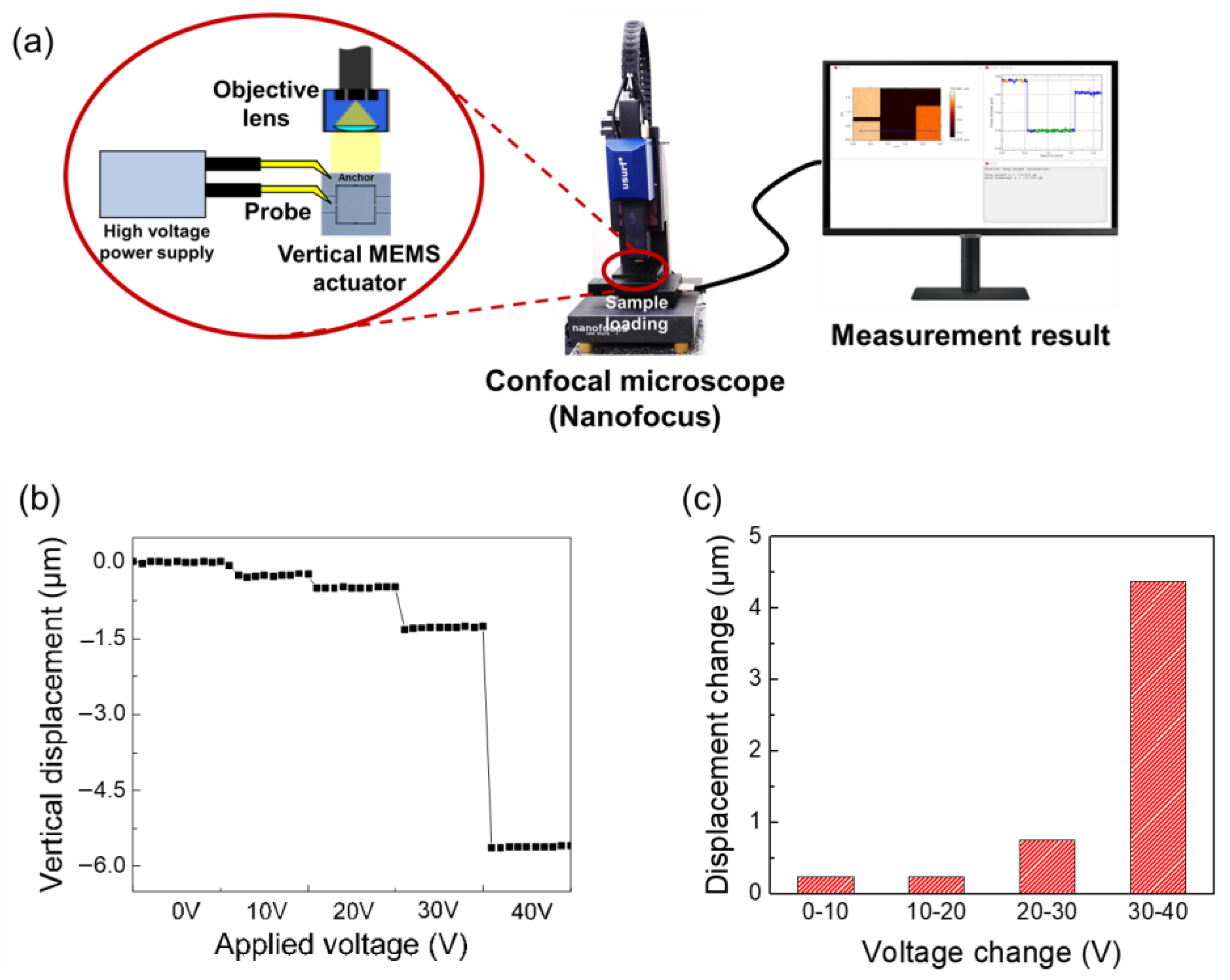
3. Results and Discussion
4. Conclusions
Author Contributions
Funding
Institutional Review Board Statement
Informed Consent Statement
Conflicts of Interest
References
- Ciuti, G.; Ricotti, L.; Menciassi, A.; Dario, P. MEMS sensor technologies for human centred applications in healthcare, physical activities, safety and environmental sensing: A review on research activities in Italy. Sensors 2015, 15, 6441–6468. [Google Scholar] [CrossRef] [PubMed] [Green Version]
- Silvestri, S.; Schena, E. Micromachined flow sensors in biomedical applications. Micromachines 2012, 3, 225–243. [Google Scholar] [CrossRef]
- Berndt, D.; Muggli, J.; Wittwer, F.; Langer, C.; Heinrich, S.; Knittel, T.; Schreiner, R. MEMS-based thermal conductivity sensor for hydrogen gas detection in automotive applications. Sens. Actuators A Phys. 2020, 305, 111670. [Google Scholar] [CrossRef]
- Yoo, H.W.; Riegler, R.; Brunner, D.; Albert, S.; Thurner, T.; Schitter, G. Experimental Evaluation of Vibration Influence on a Resonant MEMS Scanning System for Automotive Lidars. IEEE Trans. Ind. Electron. 2022, 69, 3099–3108. [Google Scholar] [CrossRef]
- Sim, S.-M.; Lee, Y.; Jang, Y.-H.; Lee, Y.-S.; Kim, Y.-K.; Llamas-Garro, I.; Kim, J.-M. A 50–100 GHz ohmic contact SPDT RF MEMS silicon switch with dual axis movement. Microelectron. Eng. 2016, 162, 69–74. [Google Scholar] [CrossRef]
- Zhou, L.; Kato, F.; Nakamura, N.; Oshikane, Y.; Nagakubo, A.; Ogia, H. MEMS hydrogen gas sensor with wireless quartz crystal resonator. Sens. Actuators B Chem. 2021, 334, 129651. [Google Scholar] [CrossRef]
- Hong, V.A.; Yoneoka, S.; Messana, M.W.; Graham, A.B.; Salvia, J.C.; Branchflower, T.T.; Ng, E.J.; Kenny, T.W. Fatigue Experiments on Single Crystal Silicon in an Oxygen-Free Environment. J. Microelectromech. Syst. 2015, 24, 351–359. [Google Scholar] [CrossRef]
- Kim, J.-M.; Park, J.-H.; Baek, C.-W.; Kim, Y.-K. The SiOG-based single-crystalline silicon (SCS) RF MEMS switch with uniform characteristics. J. Microelectromech. Syst. 2004, 13, 1036–1042. [Google Scholar] [CrossRef]
- Varonaa, J.; Tecpoyotl-Torresa, M.; Hamouib, A.A. Design of MEMS vertical–horizontal chevron thermal actuators. Sens. Actuators A Phys. 2009, 153, 127–130. [Google Scholar] [CrossRef]
- Gao, X.; Yang, J.; Wu, J.; Xin, X.; Li, Z.; Yuan, X.; Shen, X.; Dong, S. Piezoelectric Actuators and Motors: Materials, Designs, and Applications. Adv. Mater. Technol. 2020, 5, 1900716. [Google Scholar] [CrossRef]
- Jiang, B.; Peng, M.; Liu, Y.; Zhou, T.; Sua, Y. The fabrication of 2D micromirror with large electromagnetic driving forces. Sens. Actuators A Phys. 2019, 286, 163–168. [Google Scholar] [CrossRef]
- Lee, Y.; Sim, S.-M.; Kim, H.; Kim, Y.-K.; Kim, J.-M. Silicon MEMS acceleration switch with high reliability using hooked latch. Microelectron. Eng. 2016, 152, 10–19. [Google Scholar] [CrossRef]
- Wang, D.; Watkins, C.; Xie, H. MEMS mirrors for LiDAR: A review. Micromachines 2020, 11, 456. [Google Scholar] [CrossRef] [PubMed]
- Paliwal, A.; Sharma, A.; Tomar, M.; Gupta, V. Room temperature detection of NO2 gas using optical sensor based on surface plasmon resonance technique. Sens. Actuators B Chem. 2015, 216, 497. [Google Scholar] [CrossRef]
- Paliwal, A.; Sharma, A.; Tomar, M.; Gupta, V. Surface plasmon resonance study on the optical sensing properties of tin oxide (SnO2) films to NH3 gas. J. Appl. Phys. 2016, 119, 164502. [Google Scholar] [CrossRef]
- Michel, D.; Xiao, F.; Alameh, K. A compact, flexible fiber-optic Surface Plasmon Resonance sensor with changeable sensor chips. Sens. Actuators B Chem. 2017, 246, 258. [Google Scholar] [CrossRef]
- Srivastava, T.; Jha, R. Black Phosphorus: A New Platform for Gaseous Sensing Based on Surface Plasmon Resonance. IEEE Photon. Technol. Lett. 2018, 30, 319. [Google Scholar] [CrossRef]
- Wang, D.; Loo, J.F.C.; Chen, J.; Yam, Y.; Chen, S.-C.; He, H.; Kong, S.K.; Ho, H.P. Recent Advances in Surface Plasmon Resonance Imaging Sensors. Sensors 2019, 19, 1266. [Google Scholar] [CrossRef] [Green Version]
- Maciel-Neto, J.O.; Fernandes, G.F.; Cavalcanti, G.O.; Llamas-Garro, I.; Kim, J.-M.; Fontana, E. Prospects for Developing Pressure and Tactile Sensors Based on Surface Plasmon Resonance. IEEE Sens. J. 2022, 22, 18620–18630. [Google Scholar] [CrossRef]
- Lee, Y.; Kim, J.; Sim, S.; Llamas-Garro, I.; Kim, J.-M. Air-Gap Interrogation of Surface Plasmon Resonance in Otto Configuration. Micromachines 2021, 12, 998. [Google Scholar] [CrossRef]
- Baidya, B.; Gupta, S.K.; Mukherjee, T. An extraction-based verification methodology for MEMS. J. Microelectromech. Syst. 2002, 11, 2–11. [Google Scholar] [CrossRef]
- Weigold, J.W.; Najafi, K.; Pang, S.W. Design and fabrication of submicrometer, single crystal Si accelerometer. J. Microelectromech. Syst. 2001, 10, 518–524. [Google Scholar] [CrossRef]
- Legtenberg, R.; Groeneveld, A.W.; Elwenspoek, M. Comb-drive actuators for large displacements. J. Micromech. Microeng. 1996, 6, 320–329. [Google Scholar] [CrossRef] [Green Version]
- Tsang, S.H.; Sameoto, D.; Foulds, I.; Leung, A.M.; Parameswaran, M. Automated assembly of hingeless 90 degrees out-of-plane microstructures. J. Micromech. Microeng. 2007, 17, 1314–1325. [Google Scholar] [CrossRef]
- Lu, Q.; Bai, J.; Wang, K.; Chen, P.; Fang, W.; Wang, C. Single Chip-Based Nano-Optomechanical Accelerometer Based on Subwavelength Grating Pair and Rotated Serpentine Springs. Sensors 2018, 18, 2036. [Google Scholar]
- Fedder, G.K. Simulation of Microelectromechanical Systems. Ph.D. Thesis, University of California at Berkeley, Berkeley, CA, USA, 1994. [Google Scholar]
- Tirumala, R.; Go, D.B. An analytical formulation for the modified Paschen’s curve. Appl. Phys. Lett. 2010, 97, 151502. [Google Scholar]
- Rollier, A.S.; Legrand, B.; Collard, D.; Buchaillot, L. The stability and pull-in voltage of electrostatic parallel-plate actuators in liquid solutions. J. Micromech. Microeng. 2006, 16, 794–801. [Google Scholar] [CrossRef]
- Lee, Y.S.; Jang, Y.H.; Kim, Y.K.; Kim, J.M. Thermal de-isolation of silicon microstructures in a plasma etching environment. J. Micromech. Microeng. 2013, 23, 025026. [Google Scholar]
- Lee, J.-Y.; Kim, S.-H.; Lim, H.-T.; Kim, C.-H.; Baek, C.-W.; Kim, Y.-K. Electric spring modeling for a comb actuator deformed by the footing effect in deep reactive ion etching. J. Micromech. Microeng. 2003, 13, 72–79. [Google Scholar] [CrossRef]


| Part | Symbol | Description | Value |
|---|---|---|---|
| Proof mass | wmass | width of proof mass | 4 mm |
| tmass | thickness of proof mass | 52 μm | |
| tgold | thickness of gold film | 200 nm | |
| Serpentine spring | ws | width of serpentine spring | 30 μm |
| la | length of connector beam | 80 μm | |
| lb | length of span beam | 1.71 mm | |
| ts | thickness of serpentine spring | 40 μm | |
| Chip | wchip | width of chip | 8.3 mm |
| tsi | thickness of silicon substrate | 58 μm | |
| tglass | thickness of glass substrate | 500 μm | |
| gair | distance of air gap | 6 μm | |
| gelec | distance between electrodes | 18 μm |
Publisher’s Note: MDPI stays neutral with regard to jurisdictional claims in published maps and institutional affiliations. |
© 2022 by the authors. Licensee MDPI, Basel, Switzerland. This article is an open access article distributed under the terms and conditions of the Creative Commons Attribution (CC BY) license (https://creativecommons.org/licenses/by/4.0/).
Share and Cite
Kim, K.; Lee, Y.; Llamas-Garro, I.; Kim, J.-M. Fabrication of Vertical MEMS Actuator with Hollow Square Electrode for SPR Sensing Applications. Sensors 2022, 22, 9490. https://doi.org/10.3390/s22239490
Kim K, Lee Y, Llamas-Garro I, Kim J-M. Fabrication of Vertical MEMS Actuator with Hollow Square Electrode for SPR Sensing Applications. Sensors. 2022; 22(23):9490. https://doi.org/10.3390/s22239490
Chicago/Turabian StyleKim, Kihyun, Yeonsu Lee, Ignacio Llamas-Garro, and Jung-Mu Kim. 2022. "Fabrication of Vertical MEMS Actuator with Hollow Square Electrode for SPR Sensing Applications" Sensors 22, no. 23: 9490. https://doi.org/10.3390/s22239490