

Hole Transport Materials for Tin-Based Perovskite Solar Cells: Properties, Progress, Prospects

Abstract
:
1. Introduction
2. Classical Hole Transport Layer: Spiro-OMeTAD

2.1. Limitations of Pure Spiro-OMeTAD
2.2. Doping of Spiro-OMeTAD
2.2.1. Spiro-OMeTAD + Li-TFSI + tBP
2.2.2. Spiro-OMeTAD + H-TFSI + tBP
2.2.3. Spiro-OMeTAD + H-TFSI + 2,6-lutidine
3. Replacement of Organic Materials for Spiro-OMeTAD
3.1. Organic PTAA
3.1.1. PTAA + LiTFSI + tBP
3.1.2. PTAA:4-Isopropyl-4′-methyldiphenyliodonium Tetrakis (Pentafluorophenyl)borate (TPFB)
3.2. Organic P3HT
3.3. Organic Small Molecule TPE
3.4. Commonly Used Hole Transfer Material Poly(3,4-thylenedioxythiophene): Polystyrene Sulfonate (PEDOT:PSS)
3.4.1. Polyethylene Glycol (PEG)-PEDOT:PSS
3.4.2. PEDOT:PSS/Poly-TPD
3.4.3. LiF/PEDOT:PSS
4. Inorganic Materials
4.1. Inorganic NiOx
4.2. Inorganic CuSCN
5. Conclusions
Author Contributions
Funding
Institutional Review Board Statement
Data Availability Statement
Acknowledgments
Conflicts of Interest
References
- Kojima, A.; Teshima, K.; Shirai, Y.; Miyasaka, T. Organometal halide perovskites as visible-light sensitizers for photovoltaic cells. J. Am. Chem. Soc. 2009, 131, 6050–6051. [Google Scholar] [CrossRef]
- Kim, H.-S.; Lee, C.-R.; Im, J.-H.; Lee, K.-B.; Moehl, T.; Marchioro, A.; Moon, S.-J.; Humphry-Baker, R.; Yum, J.-H.; Moser, J.E. Lead iodide perovskite sensitized all-solid-state submicron thin film mesoscopic solar cell with efficiency exceeding 9%. Sci. Rep. 2012, 2, 591. [Google Scholar] [CrossRef] [PubMed]
- Lee, M.M.; Teuscher, J.; Miyasaka, T.; Murakami, T.N.; Snaith, H.J. Efficient hybrid solar cells based on meso-superstructured organometal halide perovskites. Science 2012, 338, 643–647. [Google Scholar] [CrossRef]
- Park, J.; Kim, J.; Yun, H.-S.; Paik, M.J.; Noh, E.; Mun, H.J.; Kim, M.G.; Shin, T.J.; Seok, S.I. Controlled growth of perovskite layers with volatile alkylammonium chlorides. Nature 2023. [Google Scholar] [CrossRef]
- Im, J.-H.; Lee, C.-R.; Lee, J.-W.; Park, S.-W.; Park, N.-G. 6.5% efficient perovskite quantum-dot-sensitized solar cell. Nanoscale 2011, 3, 4088–4093. [Google Scholar] [CrossRef] [PubMed]
- Etgar, L.; Gao, P.; Xue, Z.; Peng, Q.; Chandiran, A.K.; Liu, B.; Nazeeruddin, M.K.; Grätzel, M. Mesoscopic CH3NH3PbI3/TiO2 Heterojunction Solar Cells. J. Am. Chem. Soc. 2012, 134, 17396–17399. [Google Scholar] [CrossRef]
- Heo, J.H.; Im, S.H.; Noh, J.H.; Mandal, T.N.; Lim, C.-S.; Chang, J.A.; Lee, Y.H.; Kim, H.-J.; Sarkar, A.; Nazeeruddin, M.K.; et al. Efficient inorganic–organic hybrid heterojunction solar cells containing perovskite compound and polymeric hole conductors. Nat. Photonics 2013, 7, 486–491. [Google Scholar] [CrossRef]
- Burschka, J.; Pellet, N.; Moon, S.J.; Humphry-Baker, R.; Gao, P.; Nazeeruddin, M.K.; Grätzel, M. Sequential deposition as a route to high-performance perovskite-sensitized solar cells. Nature 2013, 499, 316–319. [Google Scholar] [CrossRef]
- Liu, M.; Johnston, M.B.; Snaith, H.J. Efficient planar heterojunction perovskite solar cells by vapour deposition. Nature 2013, 501, 395–398. [Google Scholar] [CrossRef]
- Chen, Q.; Zhou, H.; Hong, Z.; Luo, S.; Duan, H.-S.; Wang, H.-H.; Liu, Y.; Li, G.; Yang, Y. Planar Heterojunction Perovskite Solar Cells via Vapor-Assisted Solution Process. J. Am. Chem. Soc. 2014, 136, 622–625. [Google Scholar] [CrossRef]
- Zhou, H.; Chen, Q.; Li, G.; Luo, S.; Song, T.-B.; Duan, H.-S.; Hong, Z.; You, J.; Liu, Y.; Yang, Y. Interface engineering of highly efficient perovskite solar cells. Science 2014, 345, 542–546. [Google Scholar] [CrossRef] [PubMed]
- Yang, W.S.; Noh, J.H.; Jeon, N.J.; Kim, Y.C.; Ryu, S.; Seo, J.; Seok, S.I. High-performance photovoltaic perovskite layers fabricated through intramolecular exchange. Science 2015, 348, 1234–1237. [Google Scholar] [CrossRef] [PubMed]
- Saliba, M.; Matsui, T.; Domanski, K.; Seo, J.Y.; Ummadisingu, A.; Zakeeruddin, S.M.; Correa-Baena, J.-P.; Tress, W.R.; Abate, A.; Hagfeldt, A.; et al. Incorporation of rubidium cations into perovskite solar cells improves photovoltaic performance. Science 2016, 354, 206–209. [Google Scholar] [CrossRef] [PubMed]
- Jeon, N.J.; Na, H.; Jung, E.H.; Yang, T.-Y.; Lee, Y.G.; Kim, G.; Shin, H.-W.; Il Seok, S.; Lee, J.; Seo, J. A fluorene-terminated hole-transporting material for highly efficient and stable perovskite solar cells. Nat. Energy 2018, 3, 682–689. [Google Scholar] [CrossRef]
- Yoo, J.J.; Seo, G.; Chua, M.R.; Park, T.G.; Lu, Y.; Rotermund, F.; Kim, Y.-K.; Moon, C.S.; Jeon, N.J.; Correa-Baena, J.-P.; et al. Efficient perovskite solar cells via improved carrier management. Nature 2021, 590, 587–593. [Google Scholar] [CrossRef] [PubMed]
- Hailegnaw, B.; Kirmayer, S.; Edri, E.; Hodes, G.; Cahen, D. Rain on methylammonium lead iodide based perovskites: Possible environmental effects of perovskite solar cells. J. Phys. Chem. Lett. 2015, 6, 1543–1547. [Google Scholar] [CrossRef]
- Li, J.; Cao, H.-L.; Jiao, W.-B.; Wang, Q.; Wei, M.; Cantone, I.; Lü, J.; Abate, A. Biological impact of lead from halide perovskites reveals the risk of introducing a safe threshold. Nat. Commun. 2020, 11, 310. [Google Scholar] [CrossRef] [PubMed]
- Popov, A.I.; Kotomin, E.A.; Maier, J. Analysis of self-trapped hole mobility in alkali halides and metal halides. Solid State Ion. 2017, 302, 3–6. [Google Scholar] [CrossRef]
- Pazoki, M.; Jacobsson, T.J.; Kullgren, J.; Johansson, E.M.J.; Hagfeldt, A.; Boschloo, G.; Edvinsson, T. Photoinduced Stark Effects and Mechanism of Ion Displacement in Perovskite Solar Cell Materials. ACS Nano 2017, 11, 2823–2834. [Google Scholar] [CrossRef]
- Rusevich, L.L.; Kotomin, E.A.; Zvejnieks, G.; Popov, A.I. Ab initio calculations of structural, electronic and vibrational properties of BaTiO3 and SrTiO3 perovskite crystals with oxygen vacancies. Low Temp. Phys. 2020, 46, 1185–1195. [Google Scholar] [CrossRef]
- Even, J.; Pedesseau, L.; Jancu, J.M.; Katan, C. DFT and k · p modelling of the phase transitions of lead and tin halide perovskites for photovoltaic cells. Phys. Status Solidi (RRL)–Rapid Res. Lett. 2014, 8, 31–35. [Google Scholar] [CrossRef]
- Abate, A. Perovskite Solar Cells Go Lead Free. Joule 2017, 1, 659–664. [Google Scholar] [CrossRef]
- Kaiser, W.; Ricciarelli, D.; Mosconi, E.; Alothman, A.A.; Ambrosio, F.; De Angelis, F. Stability of Tin- versus Lead-Halide Perovskites: Ab Initio Molecular Dynamics Simulations of Perovskite/Water Interfaces. J. Phys. Chem. Lett. 2022, 13, 2321–2329. [Google Scholar] [CrossRef]
- Mastrikov, Y.A.; Chuklina, N.G.; Sokolov, M.N.; Popov, A.I.; Gryaznov, D.V.; Kotomin, E.A.; Maier, J. Small radius electron and hole polarons in PbX2 (X = F, Cl, Br) crystals: A computational study. J. Mater. Chem. C 2021, 9, 16536–16544. [Google Scholar] [CrossRef]
- Noel, N.K.; Stranks, S.D.; Abate, A.; Wehrenfennig, C.; Guarnera, S.; Haghighirad, A.A.; Sadhanala, A.; Eperon, G.E.; Pathak, S.K.; Johnston, M.B.; et al. Lead-free organic-inorganic tin halide perovskites for photovoltaic applications. Energy Environ. Sci. 2014, 7, 3061–3068. [Google Scholar] [CrossRef]
- Hao, F.; Stoumpos, C.C.; Cao, D.H.; Chang, R.P.H.; Kanatzidis, M.G. Lead-free solid-state organic-inorganic halide perovskite solar cells. Nat. Photonics 2014, 8, 489–494. [Google Scholar] [CrossRef]
- Liao, Y.; Liu, H.; Zhou, W.; Yang, D.; Shang, Y.; Shi, Z.; Li, B.; Jiang, X.; Zhang, L.; Quan, L.N. Highly oriented low-dimensional tin halide perovskites with enhanced stability and photovoltaic performance. J. Am. Chem. Soc. 2017, 139, 6693–6699. [Google Scholar] [CrossRef]
- Jiang, X.Y.; Li, H.S.; Zhou, Q.L.; Wei, Q.; Wei, M.Y.; Jiang, L.Z.; Wang, Z.; Peng, Z.J.; Wang, F.; Zang, Z.H.; et al. One-Step Synthesis of SnI2 center dot(DMSO)(x) Adducts for High-Performance Tin Perovskite Solar Cells. J. Am. Chem. Soc. 2021, 143, 10970–10976. [Google Scholar] [CrossRef]
- Ren, G.; Han, W.; Deng, Y.; Wu, W.; Li, Z.; Guo, J.; Bao, H.; Liu, C.; Guo, W. Strategies of modifying spiro-OMeTAD materials for perovskite solar cells: A review. J. Mater. Chem. A 2021, 9, 4589–4625. [Google Scholar] [CrossRef]
- Green, M.A.; Ho-Baillie, A.; Snaith, H.J. The emergence of perovskite solar cells. Nat. Photonics 2014, 8, 506–514. [Google Scholar] [CrossRef]
- Bi, D.Q.; Yi, C.Y.; Luo, J.S.; Decoppet, J.D.; Zhang, F.; Zakeeruddin, S.M.; Li, X.; Hagfeldt, A.; Gratzel, M. Polymer-templated nucleation and crystal growth of perovskite films for solar cells with efficiency greater than 21%. Nat. Energy 2016, 1, 16142. [Google Scholar] [CrossRef]
- Jiang, Q.; Chu, Z.N.; Wang, P.Y.; Yang, X.L.; Liu, H.; Wang, Y.; Yin, Z.G.; Wu, J.L.; Zhang, X.W.; You, J.B. Planar-Structure Perovskite Solar Cells with Efficiency beyond 21%. Adv. Mater. 2017, 29, 1703852. [Google Scholar] [CrossRef]
- Yang, W.S.; Park, B.W.; Jung, E.H.; Jeon, N.J.; Kim, Y.C.; Lee, D.U.; Shin, S.S.; Seo, J.; Kim, E.K.; Noh, J.H.; et al. Iodide management in formamidinium-lead-halide-based perovskite layers for efficient solar cells. Science 2017, 356, 1376–1379. [Google Scholar] [CrossRef]
- Jiang, Q.; Zhao, Y.; Zhang, X.W.; Yang, X.L.; Chen, Y.; Chu, Z.M.; Ye, Q.F.; Li, X.X.; Yin, Z.G.; You, J.B. Surface passivation of perovskite film for efficient solar cells. Nat. Photonics 2019, 13, 460–466. [Google Scholar] [CrossRef]
- Kim, M.; Kim, G.H.; Lee, T.K.; Choi, I.W.; Choi, H.W.; Jo, Y.; Yoon, Y.J.; Kim, J.W.; Lee, J.; Huh, D.; et al. Methylammonium Chloride Induces Intermediate Phase Stabilization for Efficient Perovskite Solar Cells. Joule 2019, 3, 2179–2192. [Google Scholar] [CrossRef]
- Kim, G.; Min, H.; Lee, K.S.; Lee, D.Y.; Yoon, S.M.; Seok, S.I. Impact of strain relaxation on performance of alpha-formamidinium lead iodide perovskite solar cells. Science 2020, 370, 108–112. [Google Scholar] [CrossRef] [PubMed]
- Min, H.; Lee, D.Y.; Kim, J.; Kim, G.; Lee, K.S.; Kim, J.; Paik, M.J.; Kim, Y.K.; Kim, K.S.; Kim, M.G.; et al. Perovskite solar cells with atomically coherent interlayers on SnO2 electrodes. Nature 2021, 598, 444–450. [Google Scholar] [CrossRef] [PubMed]
- Zhu, G.; Yang, L.; Zhang, C.; Du, G.; Fan, N.; Luo, Z.; Zhang, X.; Zhang, J. Unveiling the Critical Role of Oxidants and Additives in Doped Spiro-OMeTAD toward Stable and Efficient Perovskite Solar Cells. ACS Appl. Energy Mater. 2022, 5, 3595–3604. [Google Scholar] [CrossRef]
- Kong, J.; Shin, Y.; Röhr, J.A.; Wang, H.; Meng, J.; Wu, Y.; Katzenberg, A.; Kim, G.; Kim, D.Y.; Li, T.-D.; et al. CO2 doping of organic interlayers for perovskite solar cells. Nature 2021, 594, 51–56. [Google Scholar] [CrossRef]
- Wang, N.; Zhou, Y.Y.; Ju, M.G.; Garces, H.F.; Ding, T.; Pang, S.P.; Zeng, X.C.; Padture, N.P.; Sun, X.W. Heterojunction-Depleted Lead-Free Perovskite Solar Cells with Coarse-Grained B-gamma-CsSnI3 Thin Films. Adv. Energy Mater. 2016, 6, 1601130. [Google Scholar] [CrossRef]
- Ke, W.J.; Priyanka, P.; Vegiraju, S.; Stoumpos, C.C.; Spanopoulos, I.; Soe, C.M.M.; Marks, T.J.; Chen, M.C.; Kanatzidis, M.G. Dopant-Free Tetrakis-Triphenylamine Hole Transporting Material for Efficient Tin-Based Perovskite Solar Cells. J. Am. Chem. Soc. 2018, 140, 388–393. [Google Scholar] [CrossRef] [PubMed]
- Kumar, M.H.; Dharani, S.; Leong, W.L.; Boix, P.P.; Prabhakar, R.R.; Baikie, T.; Shi, C.; Ding, H.; Ramesh, R.; Asta, M.; et al. Lead-Free Halide Perovskite Solar Cells with High Photocurrents Realized Through Vacancy Modulation. Adv. Mater. 2014, 26, 7122–7127. [Google Scholar] [CrossRef]
- Gupta, S.; Bendikov, T.; Hodes, G.; Cahen, D. CsSnBr3, A Lead-Free Halide Perovskite for Long-Term Solar Cell Application: Insights on SnF2 Addition. ACS Energy Lett. 2016, 1, 1028–1033. [Google Scholar] [CrossRef]
- Koh, T.M.; Krishnamoorthy, T.; Yantara, N.; Shi, C.; Leong, W.L.; Boix, P.P.; Grimsdale, A.C.; Mhaisalkar, S.G.; Mathews, N. Formamidinium tin-based perovskite with low E-g for photovoltaic applications. J. Mater. Chem. A 2015, 3, 14996–15000. [Google Scholar] [CrossRef]
- Jung, M.-C.; Raga, S.R.; Qi, Y. Properties and solar cell applications of Pb-free perovskite films formed by vapor deposition. RSC Adv. 2016, 6, 2819–2825. [Google Scholar] [CrossRef]
- Lee, S.J.; Shin, S.S.; Im, J.; Ahn, T.K.; Noh, J.H.; Jeon, N.J.; Seok, S.I.; Seo, J. Reducing Carrier Density in Formamidinium Tin Perovskites and Its Beneficial Effects on Stability and Efficiency of Perovskite Solar Cells. ACS Energy Lett. 2018, 3, 46–53. [Google Scholar] [CrossRef]
- Yokoyama, T.; Cao, D.H.; Stoumpos, C.C.; Song, T.B.; Sato, Y.; Aramaki, S.; Kanatzidis, M.G. Overcoming Short-Circuit in Lead-Free CH3NH3SnI3 Perovskite Solar Cells via Kinetically Controlled Gas-Solid Reaction Film Fabrication Process. J. Phys. Chem. Lett. 2016, 7, 776–782. [Google Scholar] [CrossRef] [PubMed]
- Xia, J.; Zhang, Y.; Xiao, C.; Brooks, K.G.; Chen, M.; Luo, J.; Yang, H.; Klipfel, N.I.D.; Zou, J.; Shi, Y.; et al. Tailoring electric dipole of hole-transporting material p-dopants for perovskite solar cells. Joule 2022, 6, 1689–1709. [Google Scholar] [CrossRef]
- Li, F.; Xie, Y.; Hu, Y.; Long, M.; Zhang, Y.; Xu, J.; Qin, M.; Lu, X.; Liu, M. Effects of Alkyl Chain Length on Crystal Growth and Oxidation Process of Two-Dimensional Tin Halide Perovskites. ACS Energy Lett. 2020, 5, 1422–1429. [Google Scholar] [CrossRef]
- Handa, T.; Yamada, T.; Kubota, H.; Ise, S.; Miyamoto, Y.; Kanemitsu, Y. Photocarrier Recombination and Injection Dynamics in Long-Term Stable Lead-Free CH3NH3SnI3 Perovskite Thin Films and Solar Cells. J. Phys. Chem. C 2017, 121, 16158–16165. [Google Scholar] [CrossRef]
- Do Kim, H.; Miyamoto, Y.; Kubota, H.; Yamanari, T.; Ohkita, H. Open-circuit Voltage Loss in CH3NH3SnI3 Perovskite Solar Cells. Chem. Lett. 2017, 46, 253–256. [Google Scholar] [CrossRef]
- Ke, W.J.; Stoumpos, C.C.; Logsdon, J.L.; Wasielewski, M.R.; Yan, Y.F.; Fang, G.J.; Kanatzidis, M.G. TiO2-ZnS Cascade Electron Transport Layer for Efficient Formamidinium Tin Iodide Perovskite Solar Cells. J. Am. Chem. Soc. 2016, 138, 14998–15003. [Google Scholar] [CrossRef]
- Ke, W.; Stoumpos Constantinos, C.; Zhu, M.; Mao, L.; Spanopoulos, I.; Liu, J.; Kontsevoi Oleg, Y.; Chen, M.; Sarma, D.; Zhang, Y.; et al. Enhanced photovoltaic performance and stability with a new type of hollow 3D perovskite {en}FASnI3. Sci. Adv. 2017, 3, e1701293. [Google Scholar] [CrossRef]
- Cao, D.H.; Stoumpos, C.C.; Yokoyama, T.; Logsdon, J.L.; Song, T.B.; Farha, O.K.; Wasielewski, M.R.; Hupp, J.T.; Kanatzidis, M.G. Thin Films and Solar Cells Based on Semiconducting Two-Dimensional Ruddlesden-Popper (CH3(CH2)3NH3)2(CH3NH3)n−1SnnI3n+1 Perovskites. ACS Energy Lett. 2017, 2, 982–990. [Google Scholar] [CrossRef]
- Ke, W.J.; Stoumpos, C.C.; Spanopoulos, I.; Mao, L.; Chen, M.; Wasielewski, M.R.; Kanatzidis, M.G. Efficient Lead-Free Solar Cells Based on Hollow {en}MASnI3 Perovskites. J. Am. Chem. Soc. 2017, 139, 14800–14806. [Google Scholar] [CrossRef]
- Song, T.B.; Yokoyama, T.; Stoumpos, C.C.; Logsdon, J.; Cao, D.H.; Wasielewski, M.R.; Aramaki, S.; Kanatzidis, M.G. Importance of Reducing Vapor Atmosphere in the Fabrication of Tin-Based Perovskite Solar Cells. J. Am. Chem. Soc. 2017, 139, 836–842. [Google Scholar] [CrossRef] [PubMed]
- Ke, W.; Stoumpos, C.C.; Spanopoulos, I.; Chen, M.; Wasielewski, M.R.; Kanatzidis, M.G. Diammonium Cations in the FASnI3 Perovskite Structure Lead to Lower Dark Currents and More Efficient Solar Cells. ACS Energy Lett. 2018, 3, 1470–1476. [Google Scholar] [CrossRef]
- Yang, Z.; Zhong, M.; Liang, Y.; Yang, L.; Liu, X.; Li, Q.; Zhang, J.; Xu, D. SnO2-C60 Pyrrolidine Tris-Acid (CPTA) as the Electron Transport Layer for Highly Efficient and Stable Planar Sn-Based Perovskite Solar Cells. Adv. Funct. Mater. 2019, 29, 1903621. [Google Scholar] [CrossRef]
- Qiu, X.F.; Jiang, Y.A.; Zhang, H.L.; Qiu, Z.W.; Yuan, S.; Wang, P.; Cao, B.Q. Lead-free mesoscopic Cs2SnI6 perovskite solar cells using different nanostructured ZnO nanorods as electron transport layers. Phys. Status Solidi-Rapid Res. Lett. 2016, 10, 587–591. [Google Scholar] [CrossRef]
- Qiu, X.F.; Cao, B.Q.; Yuan, S.; Chen, X.F.; Qiu, Z.W.; Jiang, Y.A.; Ye, Q.; Wang, H.Q.; Zeng, H.B.; Liu, J.; et al. From unstable CsSnI3 to air-stable Cs2SnI6: A lead-free perovskite solar cell light absorber with bandgap of 1.48 eV and high absorption coefficient. Sol. Energy Mater. Sol. Cells 2017, 159, 227–234. [Google Scholar] [CrossRef]
- Liao, W.Q.; Zhao, D.W.; Yu, Y.; Grice, C.R.; Wang, C.L.; Cimaroli, A.J.; Schulz, P.; Meng, W.W.; Zhu, K.; Xiong, R.G.; et al. Lead-Free Inverted Planar Formamidinium Tin Triiodide Perovskite Solar Cells Achieving Power Conversion Efficiencies up to 6.22%. Adv. Mater. 2016, 28, 9333–9340. [Google Scholar] [CrossRef]
- Fujihara, T.; Terakawa, S.; Matsushima, T.; Qin, C.; Yahiro, M.; Adachi, C. Fabrication of high coverage MASnI3 perovskite films for stable, planar heterojunction solar cells. J. Mater. Chem. C 2017, 5, 1121–1127. [Google Scholar] [CrossRef]
- Xi, J.; Wu, Z.X.; Jiao, B.; Dong, H.; Ran, C.X.; Piao, C.C.; Lei, T.; Song, T.B.; Ke, W.J.; Yokoyama, T.; et al. Multichannel Interdiffusion Driven FASnI3 Film Formation Using Aqueous Hybrid Salt/Polymer Solutions toward Flexible Lead-Free Perovskite Solar Cells. Adv. Mater. 2017, 29, 1606964. [Google Scholar] [CrossRef] [PubMed]
- Zhao, Z.R.; Gu, F.D.; Li, Y.L.; Sun, W.H.; Ye, S.Y.; Rao, H.X.; Liu, Z.W.; Bian, Z.Q.; Huang, C.H. Mixed-Organic-Cation Tin Iodide for Lead-Free Perovskite Solar Cells with an Efficiency of 8.12%. Adv. Sci. 2017, 4, 1700204. [Google Scholar] [CrossRef] [PubMed]
- Chen, K.; Wu, P.; Yang, W.Q.; Su, R.; Luo, D.Y.; Yang, X.Y.; Tu, Y.G.; Zhu, R.; Gong, Q.H. Low-dimensional perovskite interlayer for highly efficient lead-free formamidinium tin iodide perovskite solar cells. Nano Energy 2018, 49, 411–418. [Google Scholar] [CrossRef]
- Deng, L.; Wang, K.; Yang, H.; Yu, H.; Hu, B. Polymer assist crystallization and passivation for enhancements of open-circuit voltage and stability in tin-halide perovskite solar cells. J. Phys. D Appl. Phys. 2018, 51, 475102. [Google Scholar] [CrossRef]
- Kayesh, M.E.; Chowdhury, T.H.; Matsuishi, K.; Kaneko, R.; Kazaoui, S.; Lee, J.-J.; Noda, T.; Islam, A. Enhanced Photovoltaic Performance of FASnI3-Based Perovskite Solar Cells with Hydrazinium Chloride Coadditive. ACS Energy Lett. 2018, 3, 1584–1589. [Google Scholar] [CrossRef]
- Kim, H.; Lee, Y.H.; Lyu, T.; Yoo, J.H.; Park, T.; Oh, J.H. Boosting the performance and stability of quasi-two-dimensional tin-based perovskite solar cells using the formamidinium thiocyanate additive. J. Mater. Chem. A 2018, 6, 18173–18182. [Google Scholar] [CrossRef]
- Shao, S.Y.; Liu, J.; Portale, G.; Fang, H.H.; Blake, G.R.; ten Brink, G.H.; Koster, L.J.A.; Loi, M.A. Highly Reproducible Sn-Based Hybrid Perovskite Solar Cells with 9% Efficiency. Adv. Energy Mater. 2018, 8, 170201. [Google Scholar] [CrossRef]
- Zhu, Z.L.; Chueh, C.C.; Li, N.; Mao, C.Y.; Jen, A.K.Y. Realizing Efficient Lead-Free Formamidinium Tin Triiodide Perovskite Solar Cells via a Sequential Deposition Route. Adv. Mater. 2018, 30, 1703800. [Google Scholar] [CrossRef]
- Jokar, E.; Chien, C.-H.; Tsai, C.-M.; Fathi, A.; Diau, E.W.-G. Robust Tin-Based Perovskite Solar Cells with Hybrid Organic Cations to Attain Efficiency Approaching 10%. Adv. Mater. 2019, 31, 1804835. [Google Scholar] [CrossRef]
- Kamarudin, M.A.; Hirotani, D.; Wang, Z.; Hamada, K.; Nishimura, K.; Shen, Q.; Toyoda, T.; Iikubo, S.; Minemoto, T.; Yoshino, K.; et al. Suppression of Charge Carrier Recombination in Lead-Free Tin Halide Perovskite via Lewis Base Post-treatment. J. Phys. Chem. Lett. 2019, 10, 5277–5283. [Google Scholar] [CrossRef]
- Kayesh, M.E.; Matsuishi, K.; Kaneko, R.; Kazaoui, S.; Lee, J.J.; Noda, T.; Islam, A. Coadditive Engineering with 5-Ammonium Valeric Acid Iodide for Efficient and Stable Sn Perovskite Solar Cells. ACS Energy Lett. 2019, 4, 278–284. [Google Scholar] [CrossRef]
- Liao, M.; Yu, B.B.; Jin, Z.X.; Chen, W.; Zhu, Y.D.; Zhang, X.S.; Yao, W.T.; Duan, T.; Djerdj, I.; He, Z.B. Efficient and Stable FASnI3 Perovskite Solar Cells with Effective Interface Modulation by Low-Dimensional Perovskite Layer. Chemsuschem 2019, 12, 5007–5014. [Google Scholar] [CrossRef]
- Nishimura, K.; Hirotani, D.; Kamarudin, M.A.; Shen, Q.; Toyoda, T.; Iikubo, S.; Minemoto, T.; Yoshino, K.; Hayase, S. Relationship between Lattice Strain and Efficiency for Sn-Perovskite Solar Cells. ACS Appl. Mater. Interfaces 2019, 11, 31105–31110. [Google Scholar] [CrossRef]
- Qiu, J.; Xia, Y.D.; Zheng, Y.T.; Hui, W.; Gu, H.; Yuan, W.B.; Yu, H.; Chao, L.F.; Niu, T.T.; Yang, Y.G.; et al. 2D Intermediate Suppression for Efficient Ruddlesden-Popper (RP) Phase Lead-Free Perovskite Solar Cells. ACS Energy Lett. 2019, 4, 1513–1520. [Google Scholar] [CrossRef]
- Ran, C.X.; Gao, W.Y.; Li, J.R.; Xi, J.; Li, L.; Dai, J.F.; Yang, Y.G.; Gao, X.Y.; Dong, H.; Jiao, B.; et al. Conjugated Organic Cations Enable Efficient Self-Healing FASnI3 Solar Cells. Joule 2019, 3, 3072–3087. [Google Scholar] [CrossRef]
- Shao, S.Y.; Dong, J.J.; Duim, H.; ten Brink, G.H.; Blake, G.R.; Portale, G.; Loi, M.A. Enhancing the crystallinity and perfecting the orientation of formamidinium tin iodide for highly efficient Sn-based perovskite solar cells. Nano Energy 2019, 60, 810–816. [Google Scholar] [CrossRef]
- Xu, H.Y.; Jiang, Y.Z.; He, T.W.; Li, S.S.; Wang, H.H.; Chen, Y.; Yuan, M.J.; Chen, J. Orientation Regulation of Tin-Based Reduced-Dimensional Perovskites for Highly Efficient and Stable Photovoltaics. Adv. Funct. Mater. 2019, 29, 1807696. [Google Scholar] [CrossRef]
- Jiang, X.; Wang, F.; Wei, Q.; Li, H.; Shang, Y.; Zhou, W.; Wang, C.; Cheng, P.; Chen, Q.; Chen, L.; et al. Ultra-high open-circuit voltage of tin perovskite solar cells via an electron transporting layer design. Nat. Commun. 2020, 11, 1245. [Google Scholar] [CrossRef] [PubMed]
- Lee, M.; Kim, D.; Lee, Y.K.; Koo, H.; Lee, K.T.; Chung, I. Indene-C60 Bisadduct Electron-Transporting Material with the High LUMO Level Enhances Open-Circuit Voltage and Efficiency of Tin-Based Perovskite Solar Cells. ACS Appl. Energy Mater. 2020, 3, 5581–5588. [Google Scholar] [CrossRef]
- Meng, X.Y.; Wu, T.H.; Liu, X.; He, X.; Noda, T.; Wang, Y.B.; Segawa, H.; Han, L.Y. Highly Reproducible and Efficient FASnl3 Perovskite Solar Cells Fabricated with Volatilizable Reducing Solvent. J. Phys. Chem. Lett. 2020, 11, 2965–2971. [Google Scholar] [CrossRef] [PubMed]
- Nishimura, K.; Kamarudin, M.A.; Hirotani, D.; Hamada, K.; Shen, Q.; Iikubo, S.; Minemoto, T.; Yoshino, K.; Hayase, S. Lead-free tin-halide perovskite solar cells with 13% efficiency. Nano Energy 2020, 74, 104858. [Google Scholar] [CrossRef]
- Wang, C.B.; Gu, F.D.; Zhao, Z.R.; Rao, H.X.; Qiu, Y.M.; Cai, Z.L.; Zhan, G.; Li, X.Y.; Sun, B.X.; Yu, X.; et al. Self-Repairing Tin-Based Perovskite Solar Cells with a Breakthrough Efficiency Over 11%. Adv. Mater. 2020, 32, 1907623. [Google Scholar] [CrossRef] [PubMed]
- Jokar, E.; Cheng, P.Y.; Lin, C.Y.; Narra, S.; Shahbazi, S.; Diau, E.W.G. Enhanced Performance and Stability of 3D/2D Tin Perovskite Solar Cells Fabricated with a Sequential Solution Deposition. ACS Energy Lett. 2021, 6, 485–492. [Google Scholar] [CrossRef]
- Li, B.; Di, H.; Chang, B.; Yin, R.; Fu, L.; Zhang, Y.-N.; Yin, L. Efficient Passivation Strategy on Sn Related Defects for High Performance All-Inorganic CsSnI3 Perovskite Solar Cells. Adv. Funct. Mater. 2021, 31, 2007447. [Google Scholar] [CrossRef]
- Wang, C.B.; Zhang, Y.T.; Gu, F.D.; Zhao, Z.R.; Li, H.S.; Jiang, H.; Bian, Z.Q.; Liu, Z.W. Illumination Durability and High-Efficiency Sn-Based Perovskite Solar Cell under Coordinated Control of Phenylhydrazine and Halogen Ions. Matter 2021, 4, 709–721. [Google Scholar] [CrossRef]
- Yu, B.-B.; Chen, Z.; Zhu, Y.; Wang, Y.; Han, B.; Chen, G.; Zhang, X.; Du, Z.; He, Z. Heterogeneous 2D/3D Tin-Halides Perovskite Solar Cells with Certified Conversion Efficiency Breaking 14%. Adv. Mater. 2021, 33, 2102055. [Google Scholar] [CrossRef] [PubMed]
- Li, H.S.; Zang, Z.H.; Wei, Q.; Jiang, X.Y.; Ma, M.Y.; Xing, Z.S.; Wang, J.T.; Yu, D.N.; Wang, F.; Zhou, W.J.; et al. High-member low-dimensional Sn-based perovskite solar cells. Sci. China-Chem. 2023, 66, 459–465. [Google Scholar] [CrossRef]
- Liu, X.; Wang, Y.B.; Xie, F.X.; Yang, X.D.; Han, L.Y. Improving the Performance of Inverted Formamidinium Tin Iodide Perovskite Solar Cells by Reducing the Energy-Level Mismatch. ACS Energy Lett. 2018, 3, 1116–1121. [Google Scholar] [CrossRef]
- Liu, X.; Wu, T.H.; Chen, J.Y.; Meng, X.Y.; He, X.; Noda, T.; Chen, H.; Yang, X.D.; Segawa, H.; Wang, Y.B.; et al. Templated growth of FASnI3 crystals for efficient tin perovskite solar cells. Energy Environ. Sci. 2020, 13, 2896–2902. [Google Scholar] [CrossRef]
- Zhao, D.; Sexton, M.; Park, H.-Y.; Baure, G.; Nino, J.C.; So, F. High-Efficiency Solution-Processed Planar Perovskite Solar Cells with a Polymer Hole Transport Layer. Adv. Energy Mater. 2015, 5, 1401855. [Google Scholar] [CrossRef]
- Boehm, A.M.; Liu, T.; Park, S.M.; Abtahi, A.; Graham, K.R. Influence of Surface Ligands on Energetics at FASnI3/C60 Interfaces and Their Impact on Photovoltaic Performance. ACS Appl. Mater. Interfaces 2020, 12, 5209–5218. [Google Scholar] [CrossRef] [PubMed]
- Dong, J.J.; Shao, S.Y.; Kahmann, S.; Rommens, A.J.; Hermida-Merino, D.; ten Brink, G.H.; Loi, M.A.; Portale, G. Mechanism of Crystal Formation in Ruddlesden-Popper Sn-Based Perovskites. Adv. Funct. Mater. 2020, 30, 2001294. [Google Scholar] [CrossRef]
- Yu, Y.; Zhao, D.W.; Grice, C.R.; Meng, W.W.; Wang, C.L.; Liao, W.Q.; Cimaroli, A.J.; Zhang, H.M.; Zhu, K.; Yan, Y.F. Thermally evaporated methylammonium tin triiodide thin films for lead-free perovskite solar cell fabrication. RSC Adv. 2016, 6, 90248–90254. [Google Scholar] [CrossRef]
- Ran, C.X.; Xi, J.; Gao, W.Y.; Yuan, F.; Lei, T.; Jiao, B.; Hou, X.; Wu, Z.X. Bilateral Interface Engineering toward Efficient 2D-3D Bulk Heterojunction Tin Halide Lead-Free Perovskite Solar Cells. ACS Energy Lett. 2018, 3, 713–721. [Google Scholar] [CrossRef]
- Schulz, P.; Edri, E.; Kirmayer, S.; Hodes, G.; Cahen, D.; Kahn, A. Interface energetics in organo-metal halide perovskite-based photovoltaic cells. Energy Environ. Sci. 2014, 7, 1377–1381. [Google Scholar] [CrossRef]
- Hou, Y.; Chen, W.; Baran, D.; Stubhan, T.; Luechinger, N.A.; Hartmeier, B.; Richter, M.; Min, J.; Chen, S.; Quiroz, C.O.R.; et al. Overcoming the Interface Losses in Planar Heterojunction Perovskite-Based Solar Cells. Adv. Mater. 2016, 28, 5112–5120. [Google Scholar] [CrossRef]
- Zuo, C.; Ding, L. Modified PEDOT Layer Makes a 1.52 V Voc for Perovskite/PCBM Solar Cells. Adv. Energy Mater. 2017, 7, 1601193. [Google Scholar] [CrossRef]
- Wolff, C.M.; Zu, F.; Paulke, A.; Toro, L.P.; Koch, N.; Neher, D. Reduced Interface-Mediated Recombination for High Open-Circuit Voltages in CH3NH3PbI3 Solar Cells. Adv. Mater. 2017, 29, 1700159. [Google Scholar] [CrossRef] [PubMed]
- Wu, C.-G.; Chiang, C.-H.; Chang, S.H. A perovskite cell with a record-high-Voc of 1.61 V based on solvent annealed CH3NH3PbBr3/ICBA active layer. Nanoscale 2016, 8, 4077–4085. [Google Scholar] [CrossRef] [PubMed]
- Wang, F.; Jiang, X.Y.; Chen, H.; Shang, Y.Q.; Liu, H.F.; Wei, J.L.; Zhou, W.J.; He, H.L.; Liu, W.M.; Ning, Z.J. 2D-Quasi-2D-3D Hierarchy Structure for Tin Perovskite Solar Cells with Enhanced Efficiency and Stability. Joule 2018, 2, 2732–2743. [Google Scholar] [CrossRef]
- Wang, T.; Zheng, F.; Tang, G.; Cao, J.; You, P.; Zhao, J.; Yan, F. 2D WSe2 Flakes for Synergistic Modulation of Grain Growth and Charge Transfer in Tin-Based Perovskite Solar Cells. Adv. Sci. 2021, 8, 2004315. [Google Scholar] [CrossRef] [PubMed]
- Cao, J.; Tai, Q.; You, P.; Tang, G.; Wang, T.; Wang, N.; Yan, F. Enhanced performance of tin-based perovskite solar cells induced by an ammonium hypophosphite additive. J. Mater. Chem. A 2019, 7, 26580–26585. [Google Scholar] [CrossRef]


| Perovskite | Device Structure | Voc (mV) | Jsc (mA/cm2) | FF (%) | PCE (%) | Ref. |
|---|---|---|---|---|---|---|
| B-γ-CsSnI3 | ITO/TiO2/PVSK/Spiro-OMeTAD/Au | 480 | 8.11 | 19.80 | 0.77 | [40] |
| en-FASnI3 | FTO/c-TiO2/mp-TiO2/PVSK/Spiro-OMeTAD/Au | 429 | 13.38 | 30.79 | 1.77 | [41] |
| CsSnI3 + 20 mol%SnF2 | FTO/c-TiO2/mp-TiO2/PVSK/Spiro-OMeTAD/Au | 240 | 25.80 | 30.00 | 1.87 | [42] |
| CsSnBr3 | FTO/c-TiO2/mp-TiO2/PVSK/Spiro-OMeTAD + Li-TFSI + tBP/Au | 410 | 9.00 | 58.00 | 2.10 | [43] |
| FASnI3 | FTO/TiO2+PVSK/Spiro-OMeTAD + Li-TFSI + tBP/Au | 238 | 24.45 | 36.00 | 2.10 | [44] |
| MASnBr3 | FTO/c-TiO2/PVSK/Spiro-OMeTAD + Li-TFSI + tBP/Au | 236 | 0.03 | 25.60 | 0.002 | [45] |
| MASnI3 | FTO/c-TiO2/mp-TiO2/PVSK/Spiro-OMeTAD + H-TFSI + tBP/Au | 880 | 16.8 | 42.00 | 6.40 | [25] |
| MASnI3 | FTO/c-TiO2/mp-TiO2/PVSK/Spiro-OMeTAD + H-TFSI + 2,6-lutidine/Au | 680 | 16.30 | 48.00 | 5.23 | [26] |
| MASnI2Br | FTO/c-TiO2/mp-TiO2/PVSK/Spiro-OMeTAD + H-TFSI + 2,6-lutidine/Au | 770 | 14.38 | 50.00 | 5.48 | [26] |
| MASnIBr2 | FTO/c-TiO2/mp-TiO2/PVSK/Spiro-OMeTAD + H-TFSI + 2,6-lutidine/Au | 820 | 12.30 | 57.00 | 5.73 | [26] |
| MASnBr3 | FTO/c-TiO2/mp-TiO2/PVSK/Spiro-OMeTAD + H-TFSI + 2,6-lutidine/Au | 880 | 8.26 | 59.00 | 4.27 | [26] |
| FASnI3(25mol% Br) | FTO/c-TiO2/mp-TiO2/PVSK/Spiro-OMeTAD + H-TFSI + 2,6-lutidine/Au | 414 | 19.80 | 66.90 | 5.50 | [46] |
| Perovskite | Device Structure | Voc (mV) | Jsc (mA/cm2) | FF (%) | PCE (%) | Ref. |
|---|---|---|---|---|---|---|
| BA2(FA)n-1SnnI3n+1 | FTO/c-TiO2/mp-TiO2/BA-PVSK/PTAA + Li-TFSI + tBP/Au | 420 | 23.98 | 40.21 | 4.04 | [49] |
| OA2(FA)n-1SnnI3n+1 | FTO/c-TiO2/mp-TiO2/OA-PVSK/PTAA + Li-TFSI + tBP/Au | 391 | 20.21 | 37.84 | 2.99 | [49] |
| DA2(FA)n-1SnnI3n+1 | FTO/c-TiO2/mp-TiO2/DA-PVSK/PTAA + Li-TFSI + tBP/Au | 325 | 16.48 | 44.95 | 2.41 | [49] |
| MASnI3 | FTO/c-TiO2/mp-TiO2/PVSK/PTAA + Li-TFSI + tBP/Au | 300 | 26.10 | 30.00 | 1.90 | [50] |
| MASnI3 | FTO/c-TiO2/mp-TiO2/PVSK/PTAA + Li-TFSI + tBP/Au | 230 | 26.00 | 39.00 | 2.30 | [51] |
| FASnI3 | FTO/c-TiO2/mp-TiO2/PVSK/PTAA + TPFB/Au | 380 | 23.09 | 60.00 | 5.27 | [52] |
| en-FASnI3 | FTO/c-TiO2/mp-TiO2/PVSK/PTAA + TPFB/Au | 480 | 22.54 | 65.96 | 7.14 | [53] |
| MASnI3 | FTO/c-TiO2/mp-TiO2/PVSK/PTAA + TPFB/Au | 273 | 17.80 | 39.00 | 1.86 | [47] |
| (BA)2MA3Sn4I13 | FTO/c-TiO2/mp-TiO2/infiltrated PVSK/PVSK capping layer/PTAA + TPFB/Au | 229 | 24.10 | 45.70 | 2.53 | [54] |
| en-MASnI3 | FTO/c-TiO2/mp-TiO2/PVSK/PTAA + TPFB/Au | 428 | 24.28 | 63.72 | 6.63 | [55] |
| MASnI3 | FTO/c-TiO2/mp-TiO2/PVSK/PVSK/PTAA + TPFB/Au | 378 | 19.92 | 51.73 | 3.89 | [56] |
| FASnI3(10%PN) | FTO/c-TiO2/mp-TiO2/PVSK/PTAA + TPFB/Au | 435 | 22.15 | 60.67 | 5.85 | [57] |
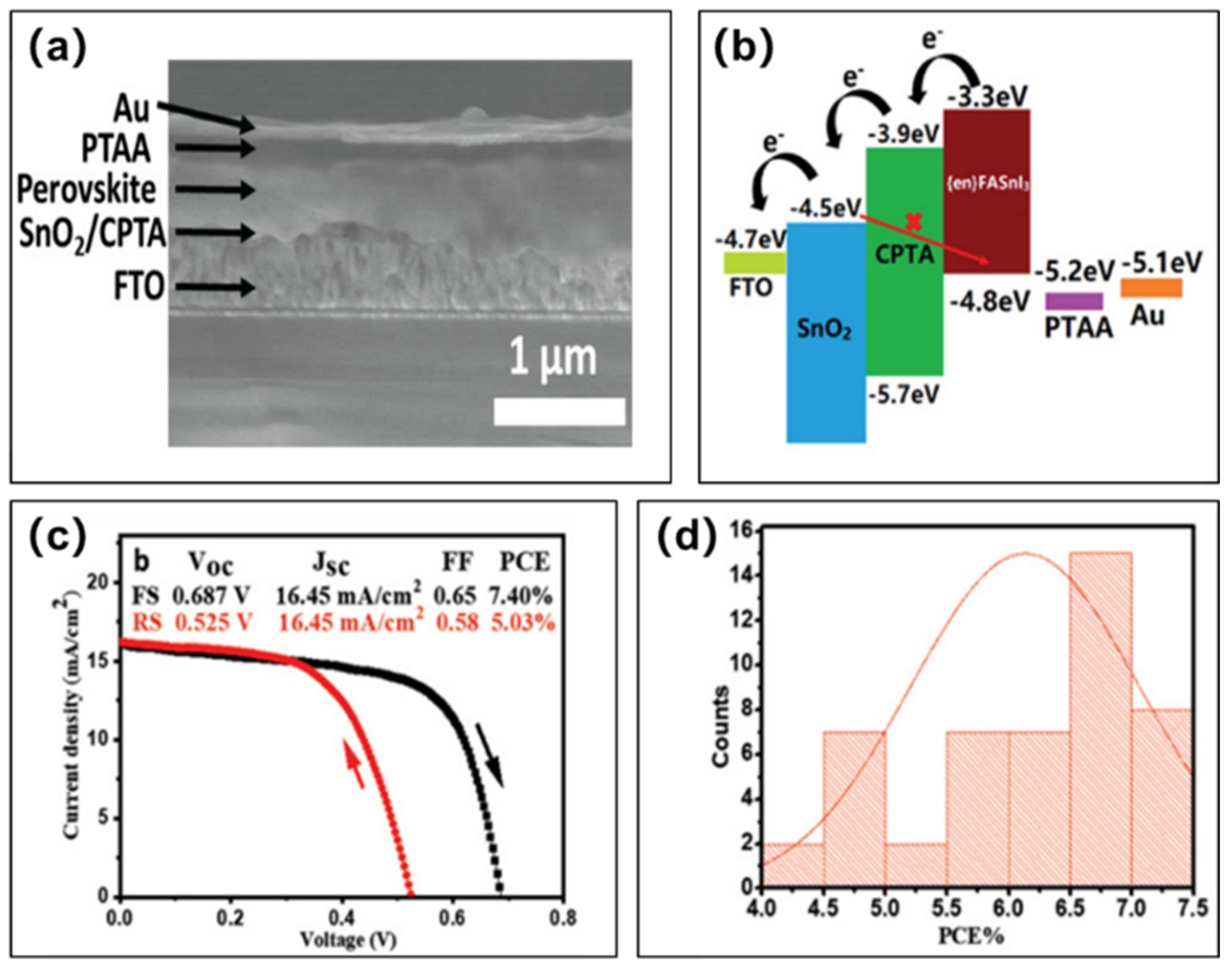
| en-FASnI3 | FTO/SnO2-CPTA/PVSK/PTAA + TPFB/Au | 720 | 16.45 | 65.00 | 7.40 | [58] |
| MASnBr3 | FTO/c-TiO2/PVSK/P3HT/Au | 498 | 4.27 | 49.10 | 1.12 | [45] |
| Cs2SnI6 | FTO/c-ZnO/n-ZnO/PVSK/P3HT/Ag | 520 | 3.20 | 51.50 | 1.00 | [59] |
| Cs2SnI6 | FTO/TiO2/PVSK/P3HT/Ag | 510 | 5.41 | 35.00 | 1.00 | [60] |
| en-FASnI3 | FTO/c-TiO2/mp-TiO2/en-FASnI3/TPE/Au | 453 | 22.60 | 67.00 | 6.85 | [41] |
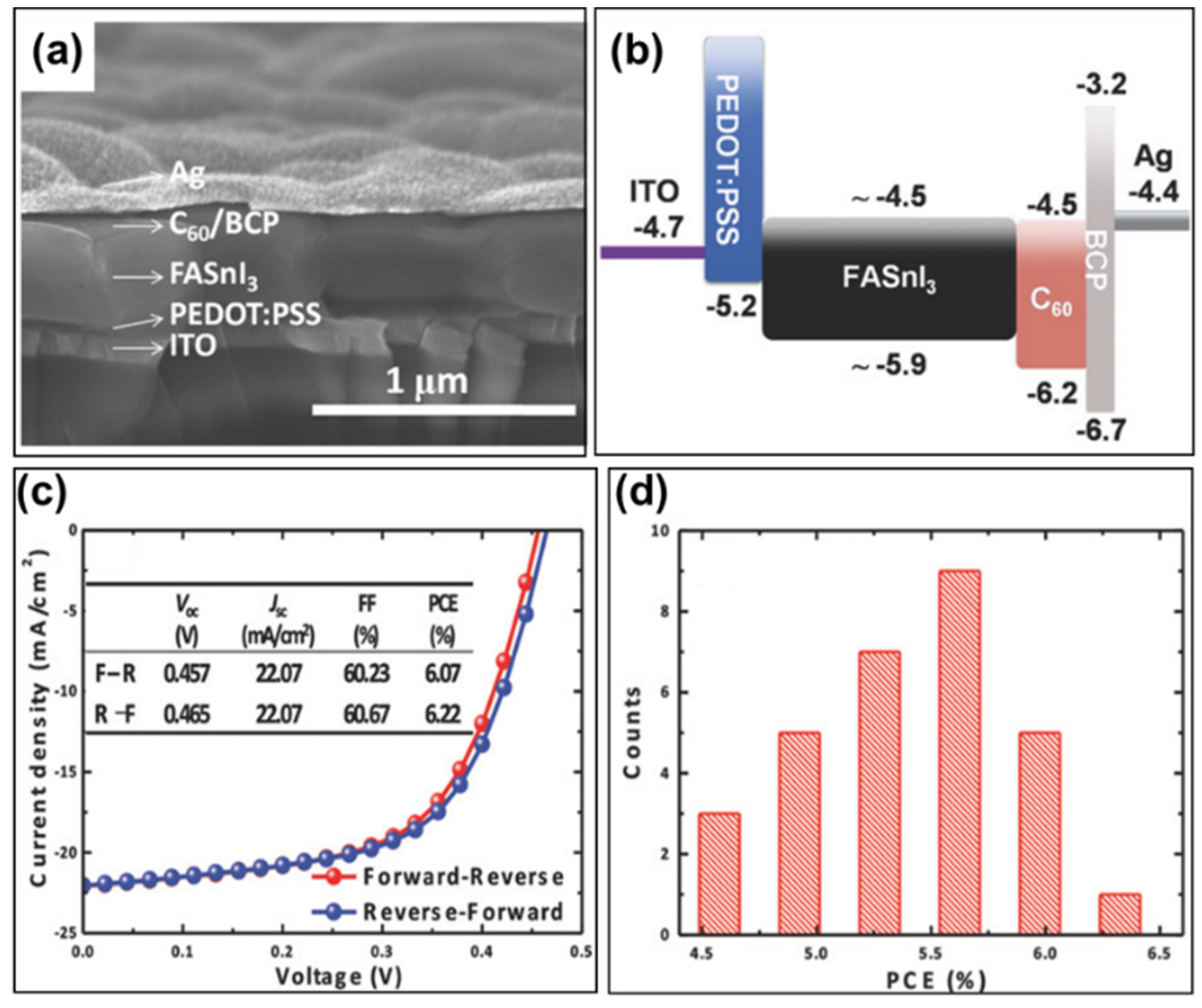
| FASnI3(10mol%SnF2) | ITO/PEDOT:PSS/PVSK/C60/BCP/Ag | 465 | 22.07 | 60.00 | 6.22 | [61] |
| MASnI3(LT-Mix) | ITO/PEDOT:PSS/MASnI3/C60/BCP/Ag | 450 | 11.82 | 40.00 | 2.14 | [62] |
| PP-FASnI3 | ITO/PEDOT:PSS/PP-FASnI3/C60/BCP/Ag | 330 | 17.78 | 67.9 | 3.98 | [63] |
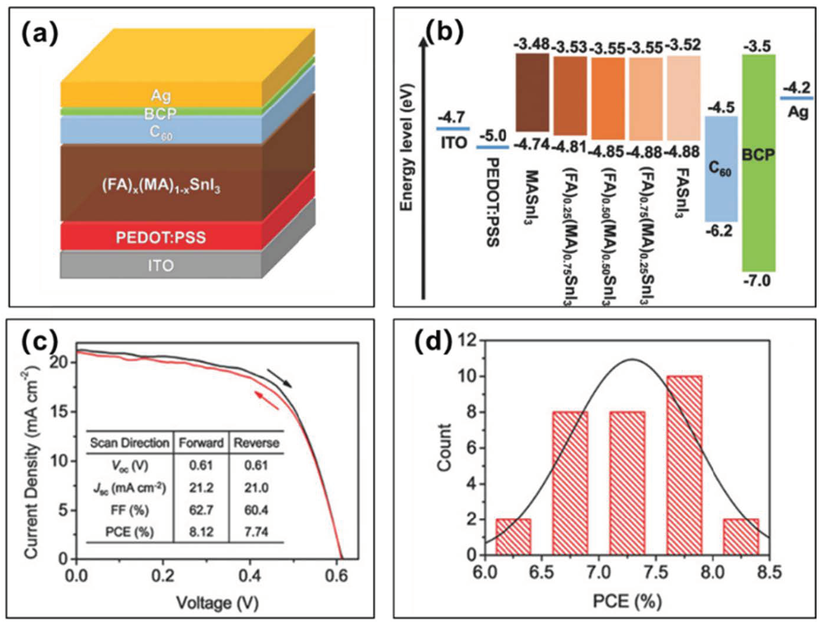
| (FA)0.75(MA)0.25SnI3 | ITO/PEDOT:PSS/PVSK/C60/BCP/Ag | 610 | 21.20 | 62.70 | 8.12 | [64] |
| FASnI3 | ITO/PEDOT:PSS/FASnI3/C60/BCP/Cu | 450 | 24.87 | 63.00 | 7.05 | [65] |
| FASnI3:PMMA | ITO/PEDOT:PSS/FASnI3:PMMA/PCBM/Ag | 482 | 13.17 | 57.00 | 3.62 | [66] |
| FASnI3(2.5%N2H5Cl) | ITO/PEDOT:PSS/FASnI3/PCBM/BCP/Ag | 455 | 17.63 | 67.30 | 5.40 | [67] |
| (PEAI)0.1FA0.9SnI3(5%FASCN) | ITO/PEDOT:PSS/PVSK/PCBM/Al | 530 | 21.80 | 66.50 | 7.66 | [68] |
| (PEAI)0.08FA0.92SnI3 | ITO/PEDOT:PSS/PVSK/C60/BCP/Al | 525 | 24.10 | 71.00 | 9.00 | [69] |
| FASnI3 + SnF2 + TMA | ITO/PEDOT:PSS/FASnI3/C60:1 wt% TBAI/Ag | 470 | 22.45 | 67.80 | 7.09 | [70] |
| GAxFA(0.98−x)SnI3–1% EDAI2 | ITO/PEDOT:PSS/PVSK/C60/BCP/Ag | 619 | 21.20 | 72.90 | 9.60 | [71] |
| FA0.98EDA0.01SnI3(0.05 mM DAE) | FTO/PEDOT:PSS/PVSK/C60/BCP/Ag/Au | 600 | 23.09 | 73.00 | 10.18 | [72] |
| FASnI3(3%5-AVAI) | ITO/PEDOT:PSS/FASnI3/PCBM/BCP/Ag | 592 | 18.89 | 62.30 | 7.00 | [73] |
| FASnI3(PEABr) | ITO/PEDOT:PSS/PVSK/PCBM/BCP/Al/Ag | 540 | 22.64 | 64.00 | 7.86 | [74] |
| EA0.1(FA0.75MA0.25)0.9SnI3 | ITO/PEDOT:PSS/PVSK/PCBM/C60/BCP/Ag/Au | 470 | 17.45 | 66.00 | 5.41 | [75] |
| (BA0.5PEA0.5)2FA3Sn4I13 | ITO/PEDOT:PSS/PVSK/C60/LiF/Al | 600 | 21.82 | 66.73 | 8.82 | [76] |
| FASnI3(15%PPAI) | ITO/PEDOT:PSS/PVSK/C60/BCP/Ag | 560 | 23.22 | 72.60 | 9.44 | [77] |
| EA0.08-FASnI3/PEA2FASn2I7 | ITO/PEDOT:PSS/PVSK/C60/BCP/Al | 510 | 23.75 | 70.00 | 8.40 | [78] |
| AVA2FAn−1SnnI3n+1(10%NH4Cl) | ITO/PEDOT:PSS/PVSK/PCBM/BCP/Ag | 610 | 21.00 | 68.00 | 8.71 | [79] |
| PEAxFA1−xSnI3(NH4SCN) | ITO/PEDOT:PSS/PVSK/ICBA/BCP/Ag | 940 | 17.40 | 75.00 | 12.40 | [80] |
| FA0.9PEA0.1SnI3 | ITO/PEDOT:PSS/PVSK/ICBA BCP/Al | 651 | 16.88 | 64.00 | 7.05 | [81] |
| FASnI3-50%LFA | ITO/PEDOT:PSS/PVSK/C60/BCP/Ag | 616 | 22.08 | 72.80 | 9.90 | [82] |
| (FA0.9EA0.1)0.98EDA0.01SnI3(GeI2) | FTO/PEDOT:PSS/PVSK/C60/BCP/Ag/Au | 840 | 20.38 | 74.00 | 13.24 | [83] |
| FASnI3(5% PHCl) | ITO/PEDOT:PSS/FASnI3/C60/BCP/Ag | 760 | 23.50 | 64.00 | 11.40 | [84] |
| FA0.8GA0.2SnI3/AN2FAn−1SnnI3n+1 | ITO/PEDOT:PSS/PVSK/C60/BCP/Ag | 645 | 21.10 | 76.30 | 10.40 | [85] |
| CsSnI3 | ITO/PEDOT:PSS/CsSnI3/C60/BCP/Cu | 630 | 19.70 | 66.10 | 8.20 | [86] |
| FASnIXBr3-X(5% PhNHNH3Cl) | ITO/PEDOT:PSS/PVSK/C60/BCP/Ag | 760 | 22.95 | 70.98 | 12.38 | [87] |
| FA0.9SnI3(10% FPEABr) | ITO/PEDOT:PSS/PVSK/ICBA/BCP/Al | 828 | 24.50 | 69.40 | 14.03 | [88] |
| FASnI3 | FTO/(PEG-)PEDOT:PSS/PVSK/PCBM/BCP/Ag | 370 | 22.06 | 62.70 | 5.12 | [89] |
| TG-FASnI3 | ITO/PEG-PEDOT:PSS/PVSK/C60+BCP/Ag | 695 | 22.01 | 73.30 | 11.22 | [90] |
| MASnI3 | ITO/PEDOT:PSS/Poly-TPD/PVSK/C60/BCP/Ag | 377 | 12.10 | 36.60 | 1.70 | [91] |
| (PEA)2(FA)n-1SnnI3n+1 | ITO/LiF/PEDOT:PSS/PVSK/C60/BCP/Ag | 470 | 20.07 | 74.00 | 6.98 | [92] |
| Perovskite | Device Structure | Voc (mV) | Jsc (mA/cm2) | FF (%) | PCE (%) | Ref. |
|---|---|---|---|---|---|---|
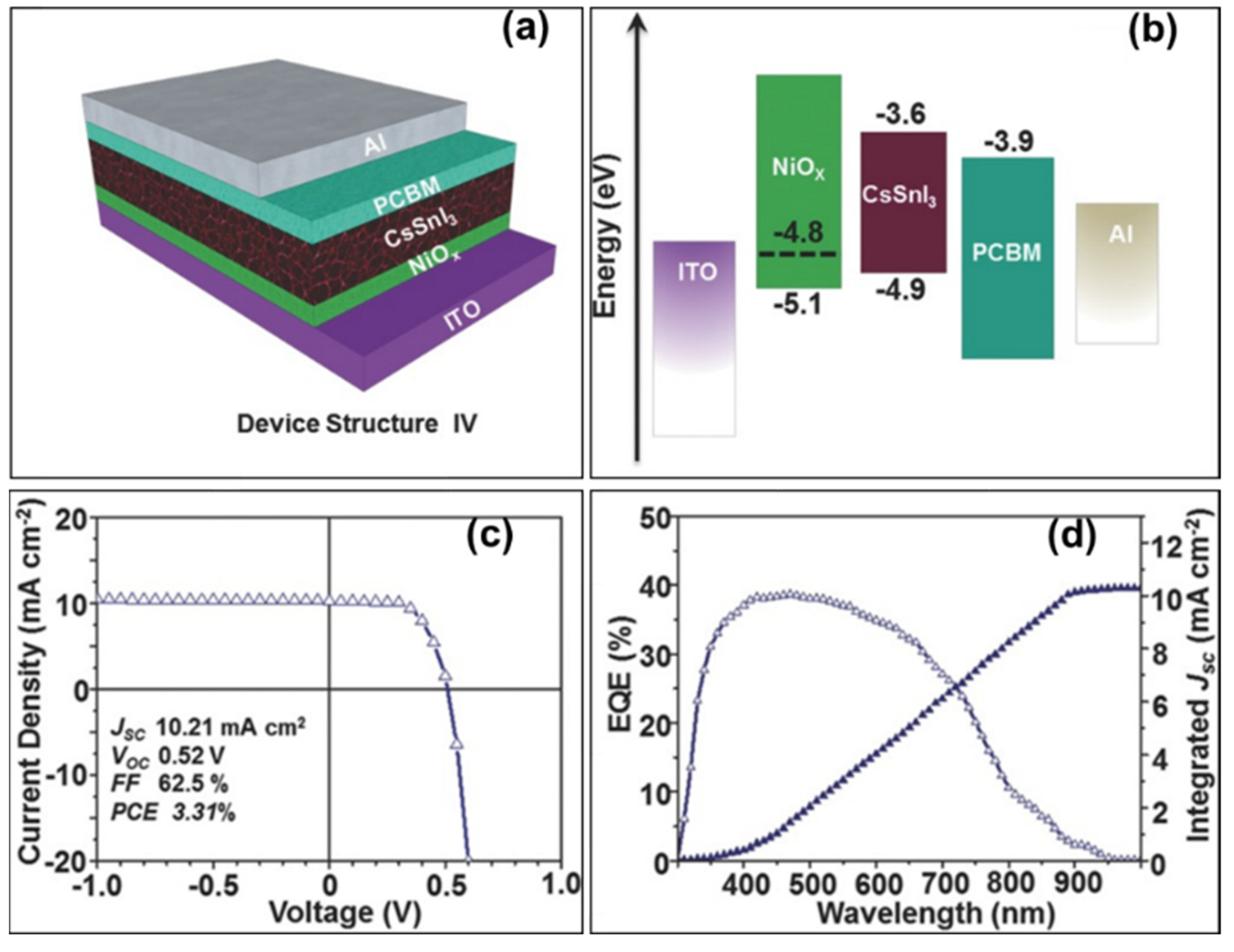
| B-γ-CsSnI3 | ITO/NiOx/PVSK/PCBM/Al | 520 | 10.21 | 62.50 | 3.31 | [40] |
| 2D(PEA2FASn2I7)/3D(FASnI3) | ITO/NiOx/PVSK/PCBM/BCP/Ag | 610 | 22.00 | 70.10 | 9.41 | [102] |
| FASnI3 | ITO/NiOx/WSe2/PVSK/PCBM/BCP/Ag | 630 | 22.71 | 73.20 | 10.47 | [103] |
| FASnI3(5 mol% AHP) | ITO/CuSCN/FASnI3/PCBM/Ag | 550 | 19.39 | 68.80 | 7.34 | [104] |
Disclaimer/Publisher’s Note: The statements, opinions and data contained in all publications are solely those of the individual author(s) and contributor(s) and not of MDPI and/or the editor(s). MDPI and/or the editor(s) disclaim responsibility for any injury to people or property resulting from any ideas, methods, instructions or products referred to in the content. |
© 2023 by the authors. Licensee MDPI, Basel, Switzerland. This article is an open access article distributed under the terms and conditions of the Creative Commons Attribution (CC BY) license (https://creativecommons.org/licenses/by/4.0/).
Share and Cite
Chen, X.; Cheng, J.; He, L.; Zhao, L.; Zhang, C.; Pang, A.; Li, J. Hole Transport Materials for Tin-Based Perovskite Solar Cells: Properties, Progress, Prospects. Molecules 2023, 28, 3787. https://doi.org/10.3390/molecules28093787
Chen X, Cheng J, He L, Zhao L, Zhang C, Pang A, Li J. Hole Transport Materials for Tin-Based Perovskite Solar Cells: Properties, Progress, Prospects. Molecules. 2023; 28(9):3787. https://doi.org/10.3390/molecules28093787
Chicago/Turabian StyleChen, Xinyao, Jin Cheng, Linfeng He, Longjiang Zhao, Chunqian Zhang, Aiying Pang, and Junming Li. 2023. "Hole Transport Materials for Tin-Based Perovskite Solar Cells: Properties, Progress, Prospects" Molecules 28, no. 9: 3787. https://doi.org/10.3390/molecules28093787