Article

Effects of Charge Compensation on Colossal Permittivity and Electrical Properties of Grain Boundary of CaCu3Ti4O12 Ceramics Substituted by Al3+ and Ta5+/Nb5+

by
Jakkree Boonlakhorn
1,2,
Jedsada Manyam
3,
Pornjuk Srepusharawoot
1,2,
Sriprajak Krongsuk
1,2 and
Prasit Thongbai
1,2,*
1
Giant Dielectric and Computational Design Research Group (GD–CDR), Department of Physics, Faculty of Science, Khon Kaen University, Khon Kaen 40002, Thailand
2
Institute of Nanomaterials Research and Innovation for Energy (IN–RIE), NANOTEC–KKU RNN on Nanomaterials Research and Innovation for Energy, Khon Kaen University, Khon Kaen 40002, Thailand
3
National Nanotechnology Center (NANOTEC), National Science and Technology Development Agency (NSTDA), Pathum Thani 12120, Thailand
*
Author to whom correspondence should be addressed.
Molecules 2021, 26(11), 3294; https://doi.org/10.3390/molecules26113294
Submission received: 1 May 2021 / Revised: 24 May 2021 / Accepted: 28 May 2021 / Published: 30 May 2021
(This article belongs to the Special Issue Review Papers in Materials Chemistry)

Abstract

:
The effects of charge compensation on dielectric and electrical properties of CaCu3Ti4-x(Al1/2Ta1/4Nb1/4)xO12 ceramics (x = 0−0.05) prepared by a solid-state reaction method were studied based on the configuration of defect dipoles. A single phase of CaCu3Ti4O12 was observed in all ceramics with a slight change in lattice parameters. The mean grain size of CaCu3Ti4-x(Al1/2Ta1/4Nb1/4)xO12 ceramics was slightly smaller than that of the undoped ceramic. The dielectric loss tangent can be reduced by a factor of 13 (tanδ ~0.017), while the dielectric permittivity was higher than 104 over a wide frequency range. Impedance spectroscopy showed that the significant decrease in tanδ was attributed to the highly increased resistance of the grain boundary by two orders of magnitude. The DFT calculation showed that the preferential sites of Al and Nb/Ta were closed together in the Ti sites, forming self-charge compensation, and resulting in the enhanced potential barrier height at the grain boundary. Therefore, the improved dielectric properties of CaCu3Ti4-x(Al1/2Ta1/4Nb1/4)xO12 ceramics associated with the enhanced electrical properties of grain boundaries. In addition, the non-Ohmic properties were also improved. Characterization of the grain boundaries under a DC bias showed the reduction of potential barrier height at the grain boundary. The overall results indicated that the origin of the colossal dielectric properties was caused by the internal barrier layer capacitor structure, in which the Schottky barriers at the grain boundaries were formed.

1. Introduction

Colossal dielectric permittivity of ceramic oxides with very large dielectric constant (ε′ > 104) has been extensively studied for use in electronics applications, especially for capacitive-based devices such as ceramic capacitors [1,2,3,4,5,6,7,8,9,10,11]. Since the colossal dielectric permittivity of CaCu3Ti4O12 (CCTO) ceramics was reported by Subramanian, et al. [12], many simple and complex oxides such as NiO, ZnO, TiO2, SnO2, BiFeO3, and CCTO-based ceramics, have been investigated [1,2,3,13,14,15,16,17,18,19,20,21,22,23,24]. However, these ceramic oxides have limitations for application in electronic devices. One of the most serious problem is a large value of the dissipation factor (tanδ) [1,2,15,25,26].
In addition, the primary causes of the colossal permittivity and nonlinear electrical response of CCTO ceramics have also been investigated due to the arguments of various models [16,27,28,29]. An internal barrier layer capacitor (IBLC) model is primarily accepted to be the origin of colossal permittivity in CCTO due to its exceptionally heterogeneous microstructure, consisting of a highly resistive layer of the grain boundaries and more conductive core inside of the grains [16,27]. However, in the case of substitution metal ions, intrinsic properties corresponding to the electronic structure and defect structures have a strong influence on the dielectric properties [28]. Therefore, an investigation on both extrinsic related-microstructure and intrinsic properties is essential.
Recently, improved colossal dielectric permittivity of these oxides can be observed in single and codoped CCTO ceramics [1,2,15,17,30,31,32,33,34,35,36]. Considering the heteroatomic substitution method, colossal permittivity with low tanδ was reported in (A5+, B3+) codoped TiO2 ceramics such as (Nb5+, In3+) [1], (Nb5+, Al3+) [35], (Nb5+, Ga3+) [34], and (Nb2+, Sc3+) [36] codoped TiO2 ceramics. Song, et al. [15] reported a high ε′ > 103 and low tanδ ~0.015 in AlxNb0.05Sn0.95-xO2.
By using the codoped concept, improved dielectric properties with low tanδ ~0.045 to 0.058 and high ε′ ~2.9 to 4.1 × 10⁴ were achieved in CaCu3Ti4-x(Nb1/2Al1/2)xO12 ceramics [2]. The investigation in codoped CCTO ceramics is of greater interest than those of other oxides because CCTO polycrystalline ceramics can also exhibit non-Ohmic properties, which can be used in varistors devices. Self-charge compensation in CaCu3Ti4-x(Nb1/2Al1/2)xO12 ceramics was proposed to be the primary cause of the enhanced colossal permittivity. However, there is still no definite evidence from the experimental and theoretical results. In addition, the question arises whether replacing some of the Nb5+ with other pentavalent ions such as Ta5+ can affect the dielectric and electrical properties of CaCu3Ti4-x(Nb1/2Al1/2)xO12 ceramics. How do the charge-compensation mechanisms occurring in the CaCu3Ti4-x(Nb1/2Al1/2)xO12, in which Nb5+ was partially replaced by Ta5+, differ from CaCu3Ti4-x(Nb1/2Al1/2)xO12 These questions should be clearly carried out. Furthermore, to achieve the colossal permittivity in codoped TiO2−, NiO−, and SnO2−based oxides, these oxides must be sintered at high temperatures (1200–1450 °C) [1,15,37]. Thus, this work aims to theoretically and experimentally describe the effects of charge-compensation mechanisms and associated formation of defects on the microstructure evolution, colossal dielectric permittivity, and electrical properties of Ta5+-doped CaCu3Ti4-x(Nb1/2Al1/2)xO12 ceramics, which were fabricated at a relatively low temperature.
In this work, CaCu3Ti4-x(Ta0.25Nb0.25Al0.5)xO12 ceramics with x = 0, 0.025, and 0.05 were prepared by a solid-state reaction method and sintered at 1090 °C for 18 h. Significantly enhanced dielectric properties of CCTO were obtained by doping with acceptor-Al3+ and donor-Nb5+/Ta5+. The first principle calculations were performed to predict the preferential sites of dopants in the CCTO structure and, hence, defect structures. Largely improved colossal dielectric properties of CaCu3Ti4-x(Ta0.25Nb0.25Al0.5)xO12 ceramics were described based on the theoretical and experimental results. The possible mechanisms of charge compensation were discussed based on the theoretical calculation.

2. Experimental Details

Nb2O5 (Sigma-Aldrich, 99.99%), Ta2O5 (Aldrich, 99.99% purity), Al2O3 (Sigma-Aldrich, 99.99% purity), CaCO3 (Sigma-Aldrich, 99.0% purity), CuO (Merck, 99.9% purity), and TiO2 (Sigma-Aldrich, 99.99% purity) are the starting raw materials for the preparation of CaCu3Ti4-x(Ta0.25Nb0.25Al0.5)xO12 ceramics. Details of the preparation method were provided in our previous publication [2]. The CaCu3Ti4-x(Ta0.25Nb0.25Al0.5)xO12 ceramic samples were obtained by sintering at 1090 °C for 18 h. The CaCu3Ti4-x(Ta0.25Nb0.25Al0.5)xO12 samples with x = 0, 0.025, and 0.05 are referred to as the CCTO, NbTaAl025, and NbTaAl05 ceramics, respectively.
The crystalline structure of samples was characterized by X-ray Diffractometer (PANalytical model EMPYREAN). The X-ray diffraction (XRD) data were collected in the 2θ range of 20–80° by using step increases of 0.02°/point. Rietveld quantitative phase analysis was carried out using the X’Pert High Score Plus v3.0e software package by PANalytical. The parameters and coefficients optimized were the zero shift, scale factor, background (with function type: polynomial), profile half-width parameters (v, u, w), lattice parameters (a, b, c), atomic site occupancies (Wyckoff), and preferred orientation parameter. Surface morphologies of samples were studied using Desktop Scanning Electron Microscopes (SEC, SNE-4500M).
The polished samples were coated by the conductive silver paint and heated in a furnace at 600 °C for 30 min using a heating rate of 5 °C/min. The dielectric properties of CaCu3Ti4-x(Ta0.25Nb0.25Al0.5)xO12 ceramics were measured by a KEYSIGHT E4990A Impedance Analyzer with an oscillation voltage of 500 mV in the frequency range of 40–107 Hz. The temperature dependence of the dielectric properties was performed in the temperature range from −60 to 210 °C. Nonlinear current density-electric field (JE) characteristics were measured using a high voltage measurement unit (Keithley model 247). The electric field breakdown (Eb) was achieved at J =1 mA.cm−2. The nonlinear coefficient (α) was calculated in the range of J = 1−10 mA.cm−2.
The preferential configuration for the Nb, Ta, and Al occupying in the Ti sites of the CCTO structure was predicted by DFT calculations. The unit cell of the CCTO structure with 40 atoms was used. Details of the calculation method are reported in our previous publication [38]. For Ta or Nb, the 5p, 6s, and 5d states were used. The 3s and 3p valence states were chosen for the Al pseudopotential.

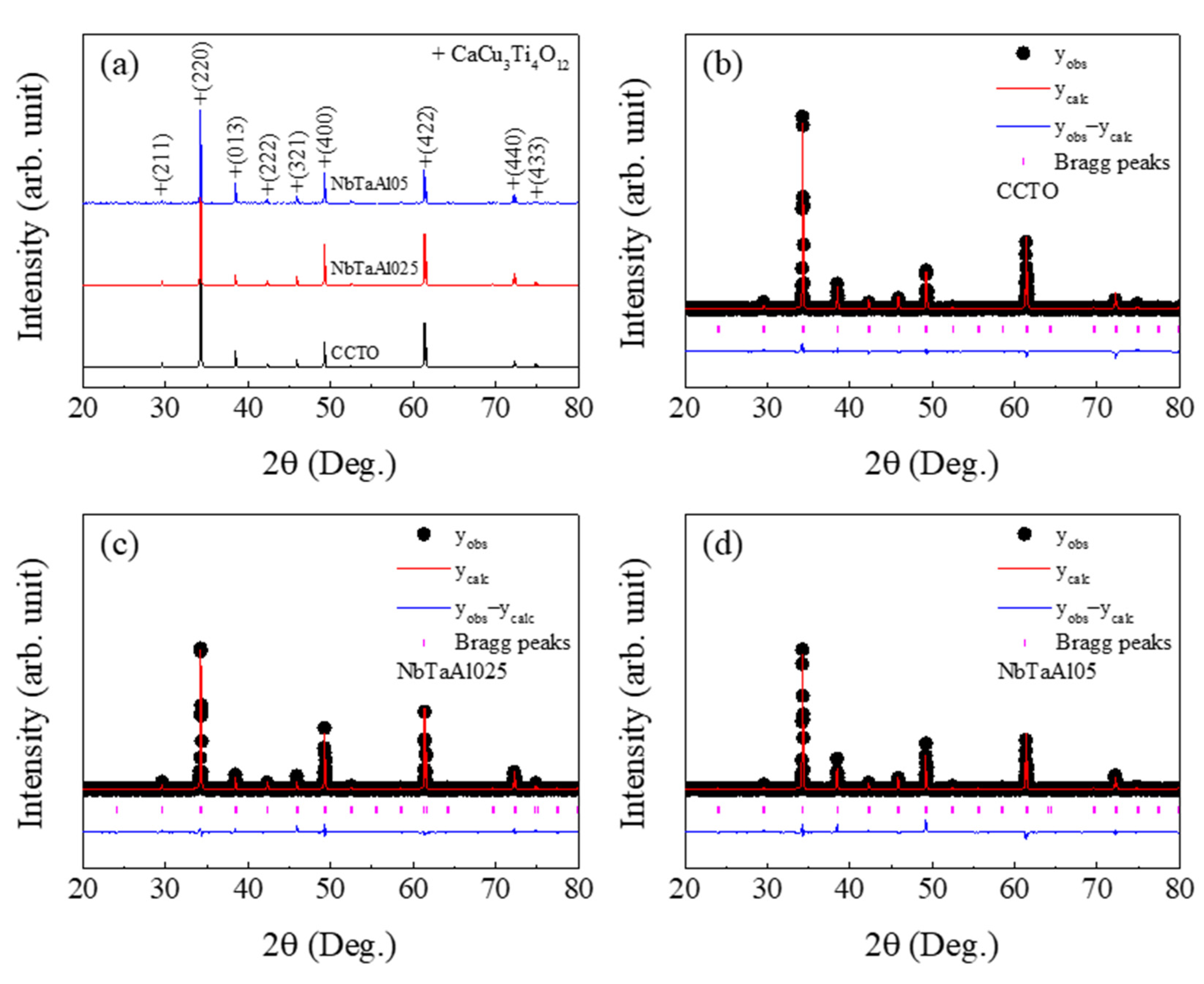
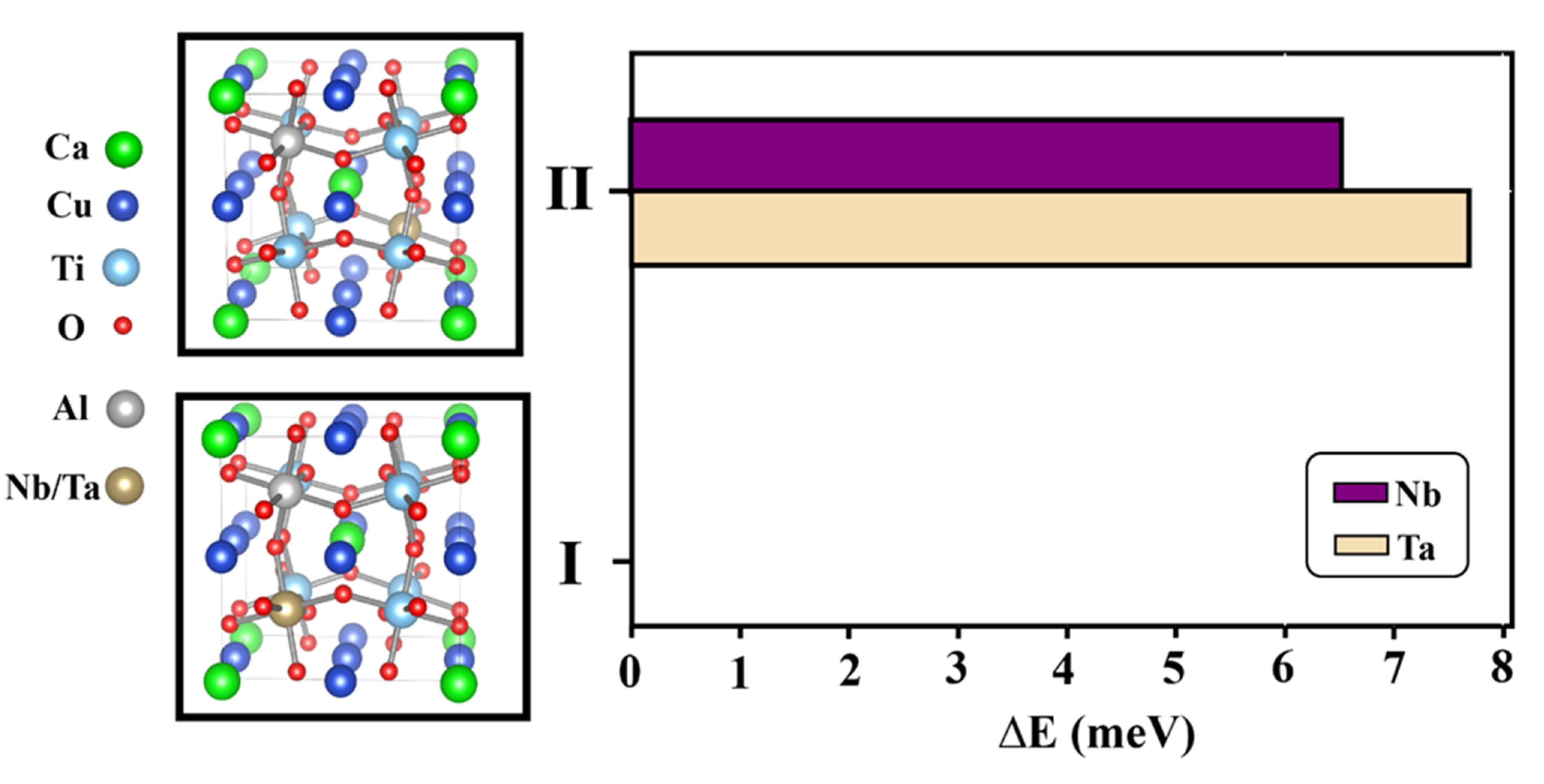
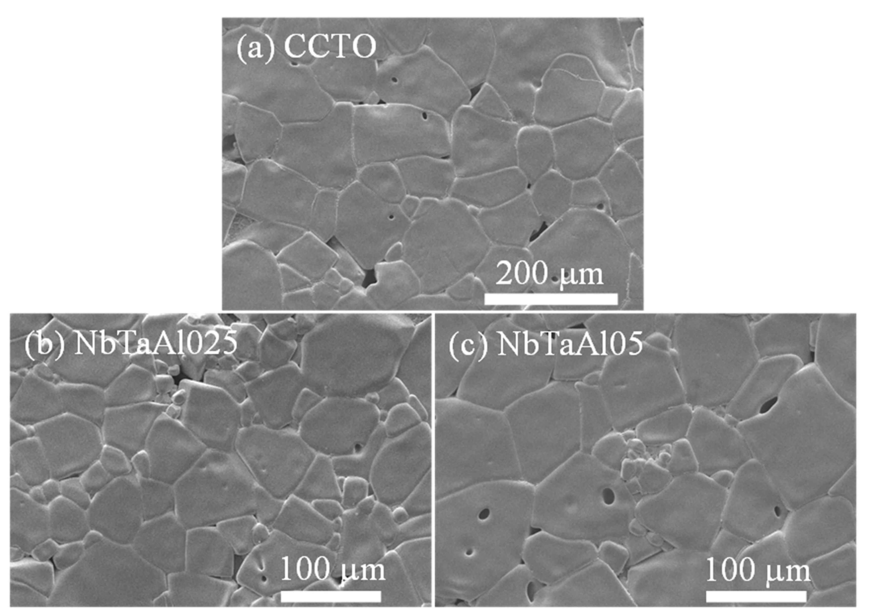
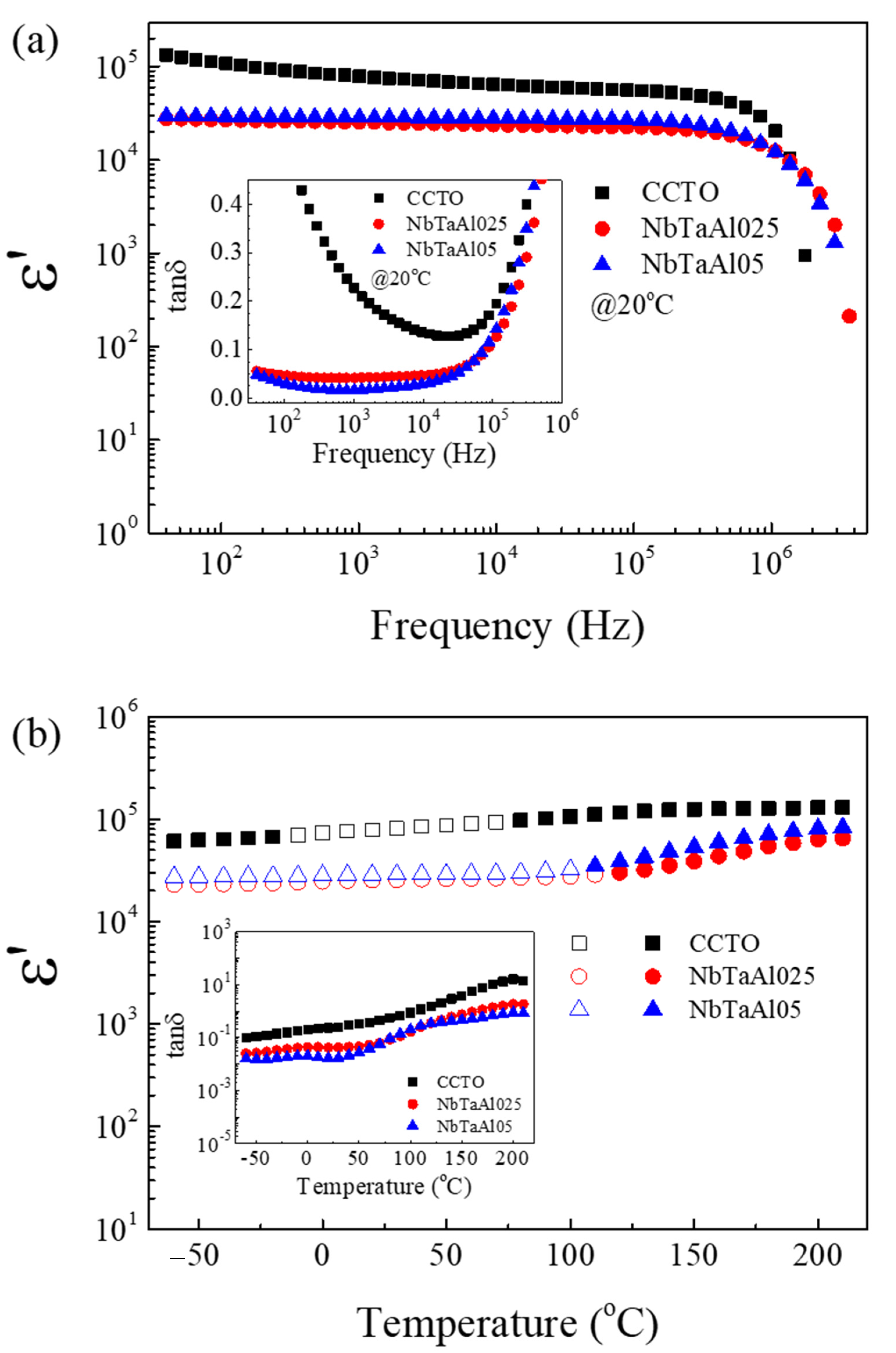
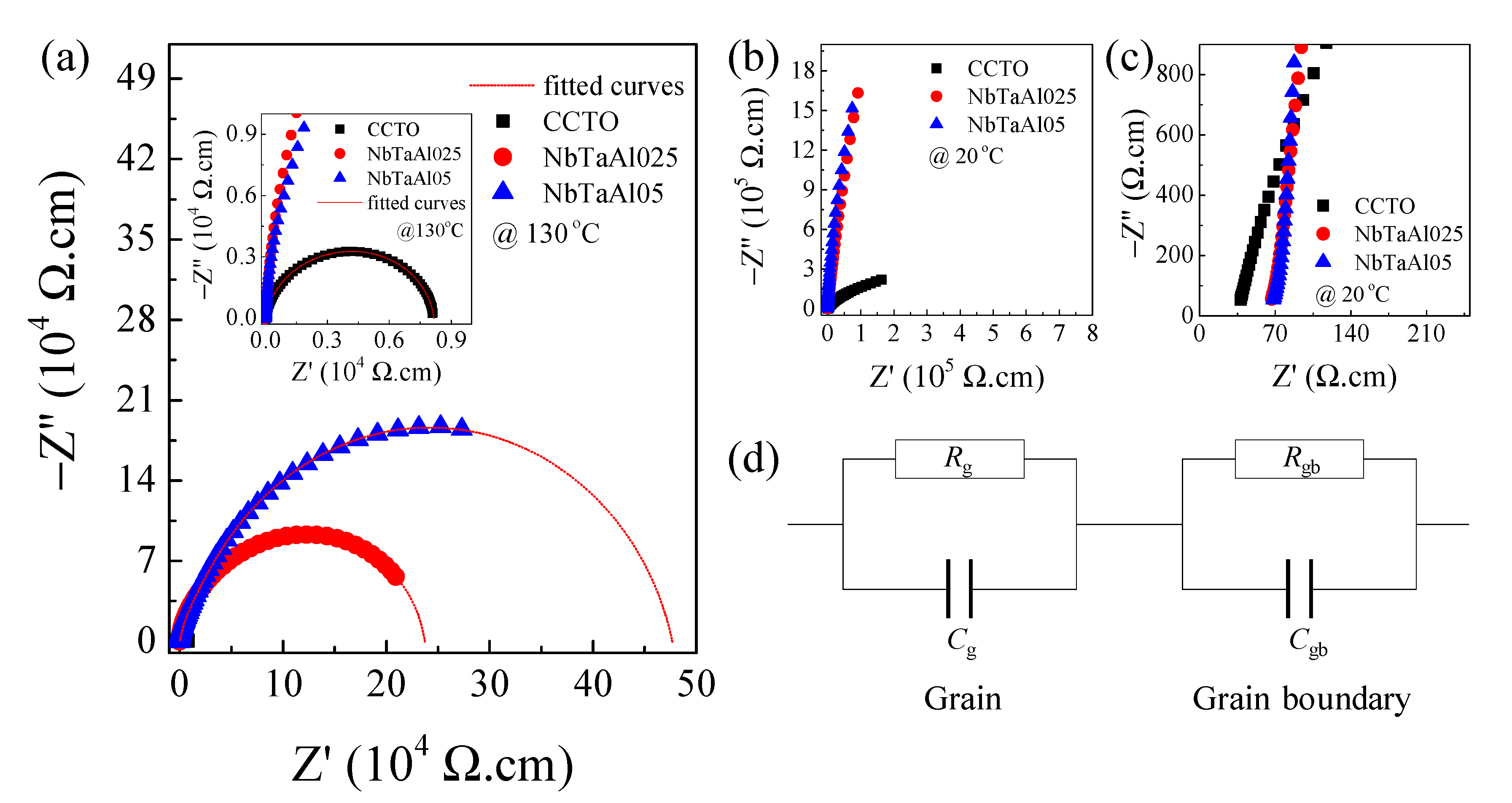
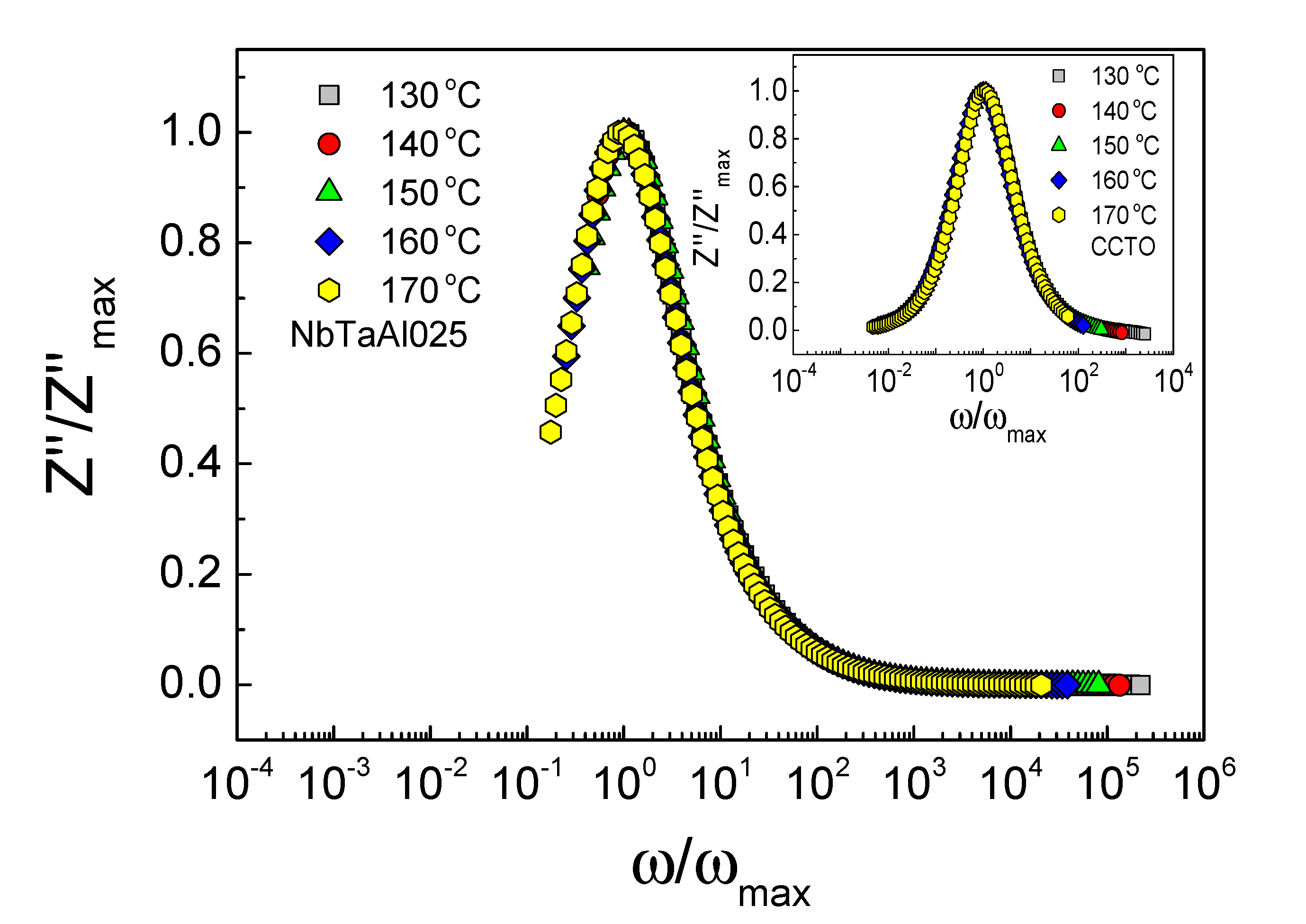
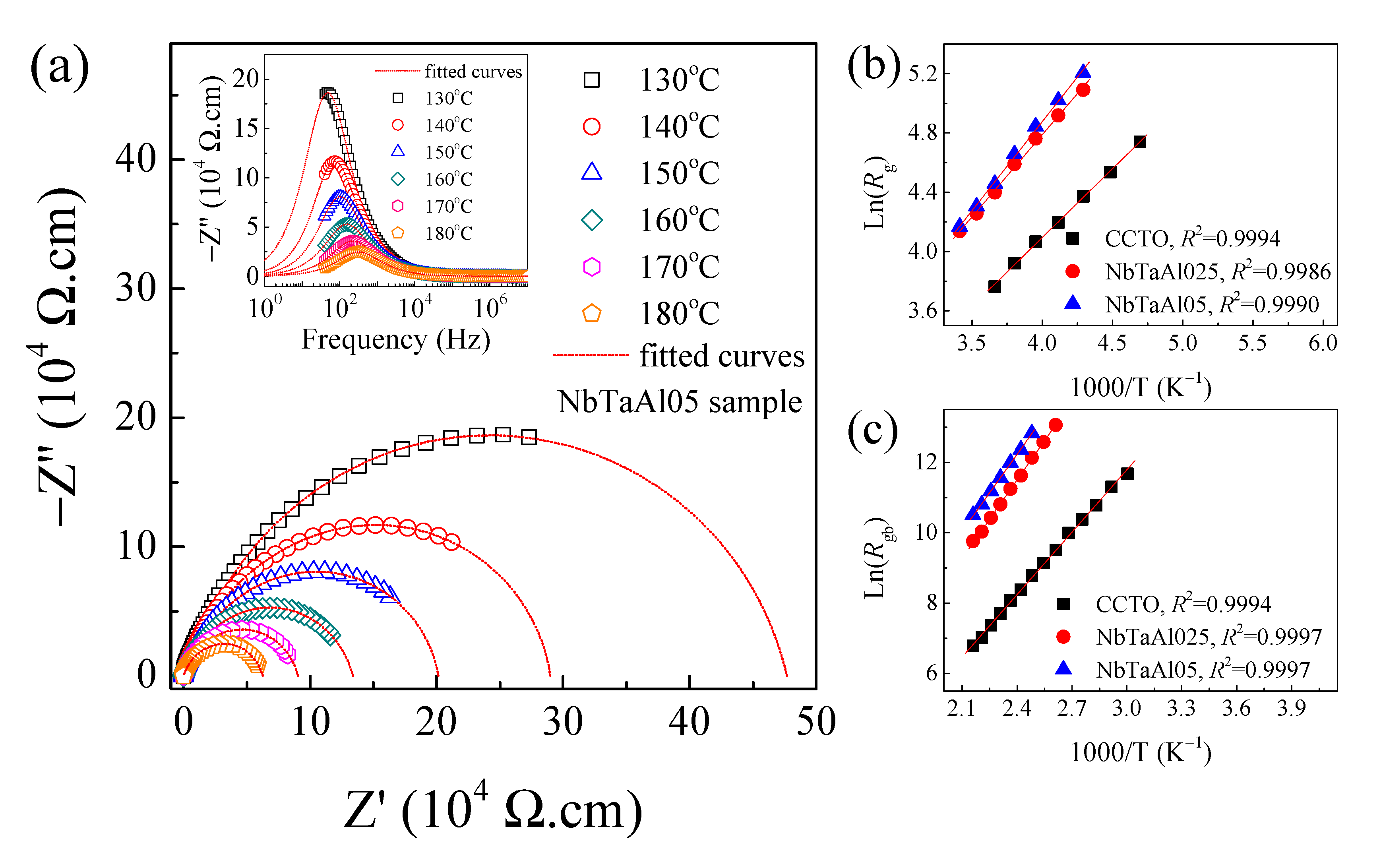
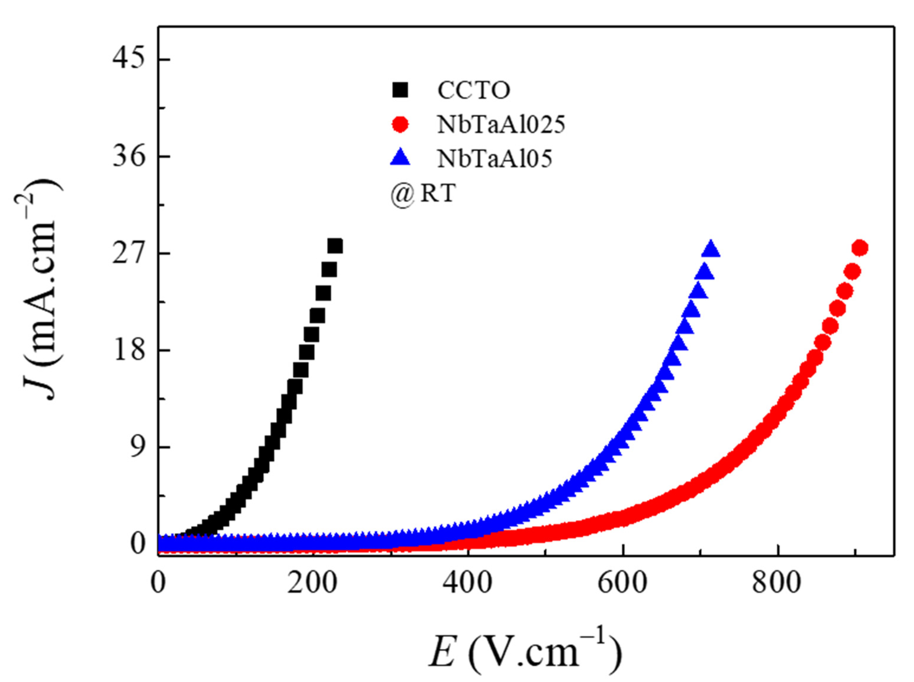
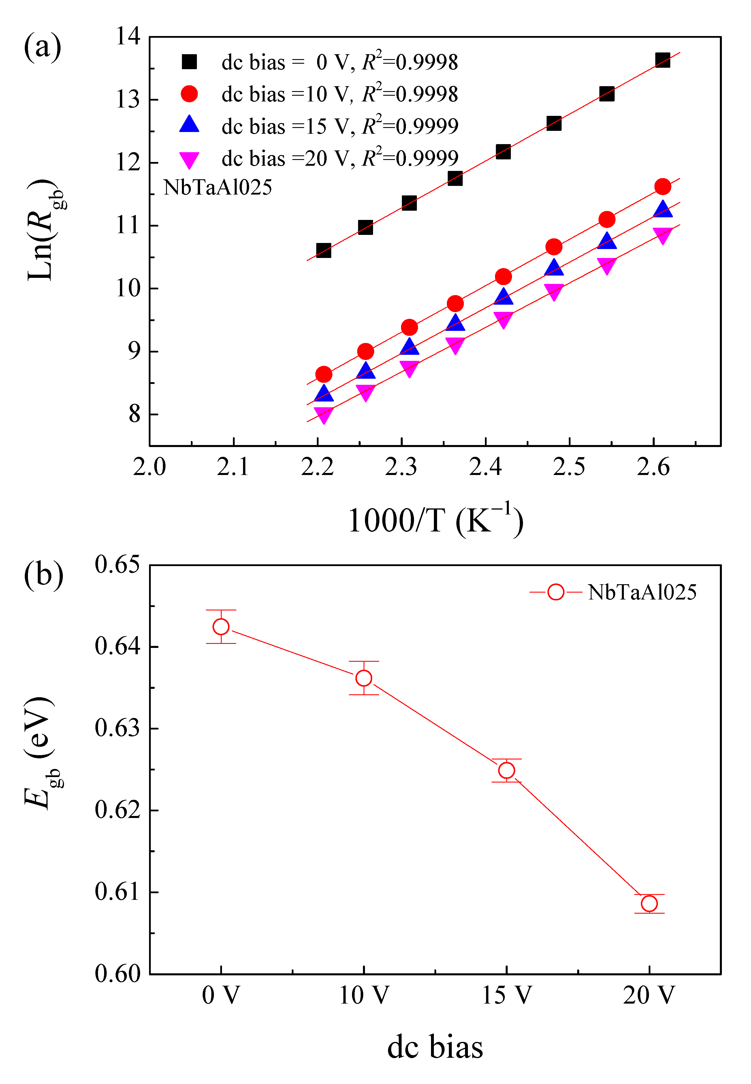
3. Results and Discussion

Identification of the crystalline structure of samples was studied using an XRD technique, as shown in Figure 1a.
A single phase of CCTO can be detected in all samples. No impurity phase related to dopant elements, e.g., Ta, Nb, and Al, is observed. As illustrated in Figure 1b–d, all the XRD patterns can be well fitted by the Rietveld method. Structural data obtained from the Rietveld refinement were given in Table 1. Rexp (expected), Rp (profile), and Rwt (weighted profile) of the CCTO, NbTaAl025, and NbTaAl05 were lower than 10, while the factor of the goodness of fit (GOF) of all samples was very low (1 < GOF < 2). Lattice parameter (a) of all the samples were nearly in a value of 7.391 Å for the standard CCTO structure [12]. The a values of the CCTO, NbTaAl025, and NbTaAl05 were 7.394, 7.393, and 7.393 Å, respectively. The a values of both the NbTaAl025 and NbTaAl05 ceramics were slightly less than that value of the CCTO ceramic. The a values of the NbTaAl025 and NbTaAl05 ceramics are equal to the a values of the CaCu3Ti4-x(Nb0.5Al0.5)xO12 ceramics with x = 0.025 and 0.05, respectively [2].
A slight change in the ɑ values of the NbTaAl025, and NbTaAl05 compared to that of the CCTO are associated with a slight difference between the average ionic radii of all the dopants of r a v e r a g e = 0.588   A ˙ (i.e., r A l 3 + = 0.535   A ˙ , r N b 5 + = 0.640   A ˙ , and r T a 5 + = 0.640   A ˙ ) and the host Ti4+ ( r T i 4 + = 0.605   A ˙ ) ion [39]. According to this result, it is likely that the dopants could completely substitute into the CCTO structure.
To further confirm the assumption for the substitution of the dopants, preferential site occupancy of the dopants and arrangement of the dopants in the structure were calculated using the DFT technique. As demonstrated in Figure 2, two different initial-defect configurations are designed in the Ti4+ sites. For both structure-I and structure-II, Nb/Ta and Al are in the octahedral sites of Ti. The positions of Nb/Ta and Al in the octahedral sites of structure-II are apart. On the other hand, the positions of Nb/Ta and Al in the octahedral sites of structure-I are closed together. According to the calculated total energies for these two structures, it can be confirmed that the Al atom is close to Nb/Ta atom in the CCTO structure (structure-I). This is because the total energy of structure-II is higher than that of structure-I. For Al and Nb in octahedral sites, the total energy difference between these two structures is 6.52 meV. Moreover, the total energy difference is 7.68 meV for the case of Al and Ta in octahedral sites. The adjacent Al-Nb and Al-Ta prefer to form in the CCTO structure.
Charge compensation is usually required for doping CCTO with Nb5+/Ta5+ into Ti4+ sites, giving rise to the reduction of Ti4+ to Ti3+ ( Ti 4 + + e Ti 3 + ) as an equation,
Nb 2 O 5 / Ta 2 O 5 + 2 TiO 2 4 TiO 2 2 Ti Ti + 2 Nb Ti / 2 Ta Ti + 8 O O + 1 / 2 O 2
Charge compensation is also required for doping CCTO with Al3+ into Ti4+ sites by the creation of an oxygen vacancy ( V O ), as illustrated by equation,
Al 2 O 3 2 TiO 2 2 Al Ti + V O + 3 V O
Equations (1) and (2) can be applied in the case of structure-II or in the cases of single-doped CCTO ceramics with Nb5+/Ta5+ or Al3+ into Ti4+ sites.
According to the DFT calculations, Al and Nb/Ta in each octahedral site prefer to close together, as demonstrated in structure-I. Charge compensation is not required due to self-charge compensation, following relation:
Nb 2 O 5 / Ta 2 O 5 + Al 2 O 3 4 TiO 2 2 Al Ti + 2 Nb Ti / 2 Ta Ti + 8 V O
The self-charge compensation mechanism may have a remarkable effect on the electrical properties of the grains and grain boundaries, resulting in the dielectric and non-Ohmic properties of the NbTaAl025 and NbTaAl05.
The SEM images of the surface microstructures of the CCTO, NbTaAl025, and NbTaAl05 are shown in Figure 3a–c. The mean grain sizes of all samples were summarized in Table 1. The mean grain sizes of the CCTO, NbTaAl025, and NbTaAl05 were 96.5 ± 25.8, 61.2 ± 13.6, and 80.7 ± 22.4 μm, respectively. The mean grain sizes of the NbTaAl025 and NbTaAl05 are smaller than that of the CCTO. According to our previous works [2,19], the grain sizes of Nb5+ and Ta5+ single-doped CCTO ceramics were reduced compared to that of the undoped CCTO. On the other hand, the grain size of CCTO ceramics was considerably enlarged by the addition of Al3+ due to the dominant effect of the oxygen vacancy diffusion (or relatively related diffusion of oxygen ions) [2]. The grain growth of polycrystalline ceramics is driven by the grain boundary mobility, which can be enhanced by increasing the diffusion rate of ions or charged species across the grain boundary. The mean grain size of the NbTaAl025 and NbTaAl05 cannot be increased compared to that of the CCTO due to the self-charge compensation mechanism (Equation (3)). Furthermore, it is possible that the substitution of Nb5+/Ta5+ ions may also be ionically compensated by cation vacancies ( V T i ). Trapped V T i in the negative space-charge region is likely related to a depletion of the intrinsic defect of oxygen vacancies in the space-charge region [40]. The diffusion rate of oxygen ions across the grain boundary is therefore reduced owing to the sizeable ionic size of oxygen ions.
The frequency dependence of ε′ and tanδ for the CCTO, NbTaAl025, and NbTaAl05 are shown in Figure 4a.
A low-frequency ε′, which was contributed from grain boundary response of these ceramics, was slightly dependent with frequency in the range of ~40 to 4 × 10⁶ Hz. The rapid decrease in ε′ at 20 °C appeared in a frequency range of >106 Hz, corresponding to the dramatically increased tanδ in a high-frequency range, as shown in its inset of Figure 4a. This dielectric behavior is referred to as the dielectric relaxation behavior, which is usually observed in CCTO ceramics [28,41,42,43]. The values of ε′ and tanδ at 1 kHz and 20 °C of all the samples were summarized in Table 2.
Clearly, the colossal dielectric properties were observed in all the samples. According to the SEM images in Figure 2, it can be suggested that the close relationship between the mean grain sizes and the low-frequency ε′ that giant dielectric response of CCTO is associated with the IBLC model [41]. Accordingly, the colossal permittivity can be expressed as
ε′ = εgbG/tgb
where G is the mean grain size, εgb and tgb are the dielectric permittivity and thickness of the GB, respectively. Thus, variation in the ε′ values should be correlated to the changes in G.
Interestingly, the low-frequency tanδ of CCTO was significantly decreased by doping with Al3+ and Nb5+/Ta5+, as demonstrated in an inset of Figure 4a (for CaCu3Ti4-x(Ta0.25Nb0.25Al0.5)xO12). The tanδ values at 1 kHz of the CCTO, NbTaAl025, and NbTaAl05 ceramics were 0.227, 0.042, and 0.017, respectively. Notably, tanδ at 1 kHz of the NbTaAl05 (x = 0.05) was reduced by a factor of 13 compared to that of the CCTO, while, at 40 Hz, tanδ was reduced by a factor of 15. Moreover, the tanδ values of the NbTaAl025 and NbTaAl05 were lower than 0.1 over the frequency range of 40−105 Hz. Strongly decreased tanδ of the doped samples may be attributed to the enhanced grain boundary properties as a result of Nb5+/Ta5+ and Al3+. According to our previous publication [2], high ε′ with low tanδ can be obtained in the CaCu3Ti4-x(Nb1/2Al1/2)xO12. It can be confirmed that by partially replacing Nb5+ with Ta5+, the improved colossal dielectric properties can be achieved. Furthermore, the tanδ can be further reduced by doping Ta5+ into CaCu3Ti4-x(Nb1/2Al1/2)xO12.
The temperature dependence of the colossal dielectric properties (ε′ and tanδ) at 1 kHz is revealed in Figure 4b and its inset. Open symbols signify the variation of ε′ in each sample of ≤±15% compared to its value at ~25 °C. The temperature stability of ε′ was improved by doping with Nb5+, Ta5+, and Al3+. The increase in ε′ in a high-temperature range is usually observed in CCTO-based ceramics [19,20,28,29,30,31,32]. As shown in the inset, the tanδ of the NbTaAl025 and NbTaAl05 were lower than that of the CCTO ceramic in over the temperature range of −60 to 210 °C. Enhancement of colossal dielectric properties as well as the temperature stability of ε′ in the NbTaAl025 and NbTaAl05 may be correlated with the enhancement of the electrical response at the grain boundaries.
To clarify the enhanced colossal dielectric properties of the NbTaAl025 and NbTaAl05, an impedance spectroscopy technique was used to study the effects of dopants on the electrical properties of the grains and grain boundaries. To analyze the impedance data, Z* plots were modelled by an ideal equivalent circuit of two parallel RC elements. The first RC element for the grain and the second element for the grain boundary response are connected in series. The complex impedance (Z*) can be calculated using the equation,
Z * = Z i Z = 1 i ω C 0 ( ε i ε )
where ε* = ε′ − ″ is the complex dielectric permittivity, ω = 2πf is the angular frequency, and C0 = ε0S/t is the capacitance of free space. S and t are the electrode area and sample thickness, respectively. The grain resistance (Rg) can be estimated from the nonzero intercept at high frequencies of the Z* plane plot, while the grain boundary resistance (Rgb) can be estimated from the diameter of a large semicircle arc [27,44]. The semicircular arcs of the NbTaAl025 and NbTaAl05 cannot be observed at a low temperature. As a result, the variation in Rgb values cannot be observed. Thus, the Z* plots at 130 °C of the CCTO, NbTaAl025, and NbTaAl05 are represented, shown in Figure 5a and its inset. It can be shown that Rgb of CCTO significantly increased with increasing dopant content. As expected, the great decrease in tanδ was due to the significantly increased Rgb values. The lowest Rgb was observed in the CCTO ceramic, as demonstrated in the inset. The Rgb values at 130 °C of the CCTO, NbTaAl025, and NbTaAl05 ceramics at 130 °C were 6.52 × 10³, 1.86 × 10⁵, and 3.74 × 10⁵ Ω·cm, respectively. The enhanced Rgb of CCTO can be created by doping with Nb5+, Ta5+, and Al3+.
As illustrated in Figure 5b, although the Rgb value cannot be calculated in the Z* plots at 20 °C, it can be reasonably indicated that Rgb at around room temperature of the NbTaAl025 and NbTaAl05 was much larger than that of the CCTO. Therefore, at 20 °C, a significantly reduced tanδ in the NbTaAl025 and NbTaAl05 was resulted from their vastly enhanced Rgb values. The close relationship between the significant increase in Rgb and a reduced tanδ is similar to those report in literature [2,17,30,31,32]. Doping CCTO with only Nb5+ or Ta5+ resulted in a significant reduction in the Rgb compared to that of the undoped CCTO [2,18,19]. However, in this current study, the addition of small Al3+ content can recover a sizeable Rgb value, which was larger than that of the undoped CCTO by two orders of magnitude. Figure 5c shows the Z* plots at high frequencies and 20 °C, showing the nonzero intercept on the Z′ axis. Accordingly, the Rg values at 20 °C of all the samples can be obtained and found to be 35, 63, and 65 Ω.cm for the CCTO, NbTaAl025, and NbTaAl05, respectively. According to Equation (1), Rg of the NbTaAl025 and NbTaAl05 should be decreased due to the introduction of free electrons. Conversely, Rg of the NbTaAl025 and NbTaAl05 increased slightly. Therefore, the effect of self-charge compensation, as predicted by the theoretical calculation, was dominant. Furthermore, few portions of V T i may be induced because the substitution of Nb5+/Ta5+ into CCTO could be ionically compensated by the creation of V T i .
The scaling behavior of Z″ in the temperature range of 130–2212170 °C was investigated, as shown in Figure 6 and the inset. The perfect overlap of all curves at different temperatures into a single curve is observed for the NbTaAl05 and CCTO ceramics. This result confirmed that the relaxation process was originated from the same mechanism.
To understand the electrical properties of the grain boundary, Z* plots at different temperatures were studied. Figure 7a and its inset show semicircle arcs of Z* plots and the frequency dependence of Z″ in the temperature range of 130–180 °C.
The diameter of the arc increased with decreasing temperature, indicating the increased Rgb value. Furthermore, the Zmax value also increased as the temperature decreased. Rg was also increased with increasing temperature (not show). The Rg and Rgb values at different temperatures can be obtained. The variations of Rg and Rgb with temperature follow the Arrhenius law [2,19,27],
R g , gb = R 0 exp ( E g ,   gb k B T )
where R0 is a pre-exponential constant term. kB and T are the Boltzmann constant and absolute temperature, respectively. Eg and Egb are the conduction activation energies of the grains and grain boundaries, respectively. As demonstrated in Figure 7b,c, the temperature dependences of Rg and Rgb are well fitted by the Arrhenius law, Equation (6). The Eg and Egb can be calculated from the slopes of the fitting lines. The Eg and Egb of all samples are summarized in Table 2. The Eg values of the CCTO, NbTaAl025, and NbTaAl05 were 0.080, 0.096, and 0.104 eV, respectively. Eg slightly changed as the doping content was different, corresponding to a slight increase in Rg. The Egb values were 0.510, 0.641, and 0.627 eV, respectively. Interestingly, Doping CCTO with Nb5+/Ta5+ and Al3+ can cause an increase in the Egb. According to the SEM images, the mean grain sizes of the NbTaAl025 and NbTaAl05 were smaller than that of the undoped CCTO. Thus, the density of the insulating grain boundaries in the NbTaAl025 and NbTaAl05 is higher than that of the CCTO. This is the first reason for the enhanced Rgb values of the NbTaAl025 and NbTaAl05. Another reason is the increase in Egb, which indicated the enhanced Schottky barrier at the grain boundaries (Фb). These are possible mechanisms on the enhanced dielectric properties in the NbTaAl025 and NbTaAl05 [2,30,31,32]. According to the IBLC model of the Schottky barrier at the grain boundaries [44], Фb is inversely proportional to the charge carrier concentration inside the semiconducting grains (Nd) or proportional to Rg. As shown in Figure 5c, a slight increase in Rg of the NbTaAl025 and NbTaAl05 was the primary cause of the increased Фb.
The nonlinear JE properties are shown in Figure 8. All the samples can exhibit the non-Ohmic characteristics of the JE curves. The breakdown electric field (Eb) and nonlinear coefficient (α) of samples were summarized in Table 2. The α values of the CCTO, NbTaAl025, and NbTaAl05 were 2.13, 5.21, and 5.02, respectively, while their Eb values were 52, 499, and 381 V·cm−1, respectively. The nonlinear JE properties of CCTO were improved by doping with Nb5+/Ta5+ and Al3+. Although Rgb of the NbTaAl05 ceramic was larger than Rgb of the NbTaAl025 ceramic, Eb of the NbTaAl05 ceramic was smaller than that of NbTaAl025 ceramic. This may be due to the effect of grain size on the NbTaAl05 was more significant than the size of NbTaAl025. The nonlinear JE properties of CCTO-based oxides were originated from the formation of the Schottky barrier at the grain boundaries. According to previous works [19,45], the non-Ohmic properties of CCTO were reduced by doping with Ta5+ and Nb5+. It was suggested that the negative charge of unknown acceptors was compensated by the positive charge of Nb5+/Ta5+, resulting in a decrease in the number of active acceptors, which lead to the existence of Фb. In this current study, the positive charges of Nb5+/Ta5+ were compensated by the effectively negative charge of 2 A l T i (Equation (3)) inside the grains without any effect on the number of active acceptors. Thus, the Фb of the NbTaAl025 and NbTaAl05 cannot be reduced by the introduction of Nb5+/Ta5+.
Characterization of the electrical response of the grain boundaries was investigated under DC bias. As illustrated in Figure 9a, Rgb of the NbTaAl025 decreased with increasing DC bias, indicating a decrease in Фb in the forward direction. At different DC bias levels, the temperature dependence of Rgb for the NbTaAl025 ceramic was well fitted by the Arrhenius law. As demonstrated in Figure 9b, Egb of the NbTaAl025 ceramic decreased with increasing DC bias. The Egb values at 0, 10, 15, and 20 DC bias voltage were 0.642 ± 0.002, 0.636 ± 0.002, 0.625 ± 0.001, and 0.609 ± 0.001 eV, respectively. As can be seen in Figure 9b, the error bars are too small, indicating the significant decrease in the Egb values as a result of DC bias. Clearly, the DC bias reduced the Egb, indicating a decrease of the potential barrier height at the grain boundaries. This result is very consistent with the results in the research work of Adams, et al. [44]. The DC bias experiment shows the close correlation between the grain boundary response and Schottky barrier response. Thus, the colossal permittivity in the CCTO-based oxides can be described by the IBLC model of the Schottky barrier at the internal insulating layer. In this model, all the grains (or grain boundaries) must show similar properties. So that all grains (or all grain boundaries) can be averaged by a single equivalent circuit component. The deviation from in the linear relationship of the Egb and DC bias voltage may be due to the different microstructures between the ideal microstructure and the fabricated microstructure of the sintered ceramics.

4. Conclusions

CaCu3Ti4-x(Al1/2Ta1/4Nb1/4)xO12 (x = 0−0.05) ceramics with a single-phase of CCTO were synthesized by a solid-state reaction method. The Nb5+/Ta5+ and Al3+ dopants had no effect on the crystal structure, while the microstructure evolution of CCTO ceramics was remarkably resulted by the dopants. Interesting, tanδ was decreased by a factor of 13 (tanδ ~0.017), while the colossal permittivity of ε′ ~ 104 was achieved. The great increase in Rgb by two orders of magnitude was the primary cause for the observed decrease in tanδ. The first principle calculations confirmed that Al and Nb/Ta were closed together in the octahedral Ti sites, leading to self-charge compensation. Фb of CCTO ceramics can be increased by doping with Nb5+/Ta5+ and Al3+ due to the self-charge compensation and the decrease in Rg. Therefore, the improved colossal dielectric properties of the NbTaAl025 and NbTaAl05 were attributed to the enhanced electrical properties of the grain boundaries. The substitution of Nb5+/Ta5+ and Al3+ into CCTO ceramics can cause improved non-Ohmic properties, which were originated by the increased Фb and increased grain boundary density. Фb was reduced by applying DC bias, indicating the formation of the Schottky barrier type. The colossal dielectric properties and non-Ohmic characteristics can be well explained based on the formation of the Schottky barrier in the IBLC structure.

Author Contributions

Conceptualization, J.B. and P.T.; Formal analysis, J.B. and P.T.; Investigation, J.B., J.M., P.S. and S.K.; Methodology, J.B.; Validation, J.B.; Visualization, P.S.; Writing—original draft, J.B. and P.T.; Writing—review & editing, P.T. All authors have read and agreed to the published version of the manuscript.

Funding

This research was supported by the Basic Research Fund of Khon Kaen University. It was partially supported by the Research Network NANOTEC (RNN) program of the National Nanotechnology Center (NANOTEC), NSTDA, Ministry of Higher Education, Science, Research, and Innovation (MHESI) (Grant No. P1851882), and Khon Kaen University, Thailand.

Institutional Review Board Statement

Not applicable.

Informed Consent Statement

Not applicable.

Data Availability Statement

The data presented in this study are available in article.

Acknowledgments

J. Boonlakhorn would like to thank the Graduate School, Khon Kaen University (Grant No. 581T211) for his Ph.D. scholarship.

Conflicts of Interest

The authors declare no conflict of interest.

Sample Availability

Not applicable.

References

  1. Hu, W.; Liu, Y.; Withers, R.L.; Frankcombe, T.J.; Norén, L.; Snashall, A.; Kitchin, M.; Smith, P.; Gong, B.; Chen, H.; et al. Electron-pinned defect-dipoles for high-performance colossal permittivity materials. Nat. Mater. 2013, 12, 821–826. [Google Scholar] [CrossRef]
  2. Boonlakhorn, J.; Kidkhunthod, P.; Chanlek, N.; Thongbai, P. (Al3+, Nb5+) co–doped CaCu3Ti4O12: An extended approach for acceptor–donor heteroatomic substitutions to achieve high–performance giant–dielectric permittivity. J. Eur. Ceram. Soc. 2018, 38, 137–143. [Google Scholar] [CrossRef]
  3. Ren, P.; He, J.; Wang, X.; Sun, M.; Zhang, H.; Zhao, G. Colossal permittivity in niobium doped BaTiO3 ceramics annealed in N2. Scr. Mater. 2018, 146, 110–114. [Google Scholar] [CrossRef]
  4. Peng, Z.; Wang, J.; Zhou, X.; Zhu, J.; Lei, X.; Liang, P.; Chao, X.; Yang, Z. Grain engineering inducing high energy storage in CdCu3Ti4O12 ceramics. Ceram. Int. 2020, 46, 14425–14430. [Google Scholar] [CrossRef]
  5. Peng, Z.; Zhou, X.; Wang, J.; Zhu, J.; Liang, P.; Chao, X.; Yang, Z. Origin of colossal permittivity and low dielectric loss in Na1/3Cd1/3Y1/3Cu3Ti4O12 ceramics. Ceram. Int. 2020, 46, 11154–11159. [Google Scholar] [CrossRef]
  6. Zhou, X.; Liang, P.; Zhu, J.; Peng, Z.; Chao, X.; Yang, Z. Enhanced dielectric performance of (Ag1/4Nb3/4)0.01Ti0.99O2 ceramic prepared by a wet-chemistry method. Ceram. Int. 2020, 46, 11921–11925. [Google Scholar] [CrossRef]
  7. Jumpatam, J.; Putasaeng, B.; Chanlek, N.; Thongbai, P. Influences of Sr2+ Doping on Microstructure, Giant Dielectric Behavior, and Non-Ohmic Properties of CaCu3Ti4O12/CaTiO3 Ceramic Composites. Molecules 2021, 26, 1994. [Google Scholar] [CrossRef] [PubMed]
  8. Boonlakhorn, J.; Putasaeng, B.; Kidkhunthod, P.; Manyam, J.; Krongsuk, S.; Srepusharawoot, P.; Thongbai, P. First-principles calculations and experimental study of enhanced nonlinear and dielectric properties of Sn4+-doped CaCu2.95Mg0.05Ti4O12 ceramics. J. Eur. Ceram. Soc. 2021, 41, 5176–5183. [Google Scholar] [CrossRef]
  9. Boonlakhorn, J.; Chanlek, N.; Manyam, J.; Krongsuk, S.; Srepusharawoot, P.; Thongbai, P. Ge4+ doped CaCu2.95Zn0.05Ti4O12 ceramics: Two-step reduction of loss tangent. Ceram. Int. 2021, 47, 17099–17108. [Google Scholar] [CrossRef]
  10. Cotrim, G.; Cortés, J.A.; Moreno, H.; Freitas, S.M.; Rezende, M.V.S.; Hein, L.R.O.; Ramírez, M.A. Tunable capacitor-varistor response of CaCu3Ti4O12/CaTiO3 ceramic composites with SnO2 addition. Mater. Charact. 2020, 170, 110699. [Google Scholar] [CrossRef]
  11. Mao, P.; Wang, J.; Xiao, P.; Zhang, L.; Kang, F.; Gong, H. Colossal dielectric response and relaxation behavior in novel system of Zr4+ and Nb5+ co-substituted CaCu3Ti4O12 ceramics. Ceram. Int. 2021, 47, 111–120. [Google Scholar] [CrossRef]
  12. Subramanian, M.A.; Li, D.; Duan, N.; Reisner, B.A.; Sleight, A.W. High Dielectric Constant in ACu3Ti4O12 and ACu3Ti3FeO12 Phases. J. Solid State Chem. 2000, 151, 323–325. [Google Scholar] [CrossRef]
  13. Siddique, M.N.; Ahmed, A.; Tripathi, P. Electric transport and enhanced dielectric permittivity in pure and Al doped NiO nanostructures. J. Alloys Compd. 2018, 735, 516–529. [Google Scholar] [CrossRef]
  14. Huang, D.; Liu, Z.; Li, Y.; Liu, Y. Colossal permittivity and dielectric relaxation of (Li, In) Co-doped ZnO ceramics. J. Alloys Compd. 2017, 698, 200–206. [Google Scholar] [CrossRef]
  15. Song, Y.; Wang, X.; Zhang, X.; Qi, X.; Liu, Z.; Zhang, L.; Zhang, Y.; Wang, Y.; Sui, Y.; Song, B. Colossal dielectric permittivity in (Al + Nb) co-doped rutile SnO2 ceramics with low loss at room temperature. Appl. Phys. Lett. 2016, 109, 142903. [Google Scholar] [CrossRef]
  16. Chung, S.-Y.; Kim, I.-D.; Kang, S.-J.L. Strong nonlinear current–voltage behaviour in perovskite-derivative calcium copper titanate. Nat. Mater. 2004, 3, 774–778. [Google Scholar] [CrossRef]
  17. Choi, S.W.; Hong, S.H.; Kim, Y.M. Effect of Al Doping on the Electric and Dielectric Properties of CaCu3Ti4O12. J. Am. Ceram. Soc. 2007, 90, 4009–4011. [Google Scholar] [CrossRef]
  18. Hong, S.-H.; Kim, D.-Y.; Park, H.-M.; Kim, Y.-M. Electric and Dielectric Properties of Nb-Doped CaCu3Ti4O12 Ceramics. J. Am. Ceram. Soc. 2007, 90, 2118–2121. [Google Scholar] [CrossRef]
  19. Thongbai, P.; Jumpatam, J.; Yamwong, T.; Maensiri, S. Effects of Ta5+ doping on microstructure evolution, dielectric properties and electrical response in CaCu3Ti4O12 ceramics. J. Eur. Ceram. Soc. 2012, 32, 2423–2430. [Google Scholar] [CrossRef]
  20. Espinoza-González, R.; Mosquera, E. Influence of micro- and nanoparticles of zirconium oxides on the dielectric properties of CaCu3Ti4O12. Ceram. Int. 2017, 43, 14659–14665. [Google Scholar] [CrossRef]
  21. Kumar, V.; Kumar, A.; Verma, M.K.; Singh, S.; Pandey, S.; Rai, V.S.; Prajapati, D.; Das, T.; Singh, N.B.; Mandal, K.D. Investigation of dielectric and electrochemical behavior of CaCu3−xMnxTi4O12 (x = 0, 1) ceramic synthesized through semi-wet route. Mater. Chem. Phys. 2020, 245, 122804. [Google Scholar] [CrossRef]
  22. Lin, H.; Xu, W.; Zhang, H.; Chen, C.; Zhou, Y.; Yi, Z. Origin of high dielectric performance in fine grain-sized CaCu3Ti4O12 materials. J. Eur. Ceram. Soc. 2020, 40, 1957–1966. [Google Scholar] [CrossRef]
  23. Moreno, H.; Cortés, J.A.; Praxedes, F.M.; Freitas, S.M.; Rezende, M.V.S.; Simões, A.Z.; Teixeira, V.C.; Ramirez, M.A. Tunable photoluminescence of CaCu3Ti4O12 based ceramics modified with tungsten. J. Alloys Compd. 2021, 850, 156652. [Google Scholar] [CrossRef]
  24. Li, T.; Sun, Y.; Dai, H.Y.; Liu, D.W.; Chen, J.; Xue, R.Z.; Chen, Z.Q. Influence of spark plasma sintering temperature on the microstructures, dielectric and I–V properties of CaCu3Ti4O12 ceramics. J. Alloys Compd. 2020, 829, 154595. [Google Scholar] [CrossRef]
  25. Peng, Z.; Liang, P.; Wang, X.; Peng, H.; Chen, X.; Yang, Z.; Chao, X. Fabrication and characterization of CdCu3Ti4O12 ceramics with colossal permittivity and low dielectric loss. Mater. Lett. 2018, 210, 301–304. [Google Scholar] [CrossRef]
  26. Jumpatam, J.; Somphan, W.; Boonlakhorn, J.; Putasaeng, B.; Kidkhunthod, P.; Thongbai, P.; Maensiri, S. Non-Ohmic Properties and Electrical Responses of Grains and Grain Boundaries of Na1/2Y1/2Cu3Ti4O12 Ceramics. J. Am. Ceram. Soc. 2017, 100, 157–166. [Google Scholar] [CrossRef]
  27. Sinclair, D.C.; Adams, T.B.; Morrison, F.D.; West, A.R. CaCu3Ti4O12: One-step internal barrier layer capacitor. Appl. Phys. Lett. 2002, 80, 2153. [Google Scholar] [CrossRef]
  28. Ni, L.; Chen, X.M. Enhanced giant dielectric response in Mg-substituted CaCu3Ti4O12 ceramics. Solid State Commun. 2009, 149, 379–383. [Google Scholar] [CrossRef]
  29. Sarkar, S.; Chaudhuri, B.K.; Yang, H.D. Nanostripe domains in CaCu[sub 3]Ti[sub 4]O[sub 12]: Its origin and influences on high permittivity response. J. Appl. Phys. 2010, 108, 014114. [Google Scholar] [CrossRef]
  30. Huang, X.; Zhang, H.; Lai, Y.; Li, J. The lowered dielectric loss tangent and grain boundary effects in fluorine-doped calcium copper titanate ceramics. Appl. Phys. A 2017, 123, 317. [Google Scholar] [CrossRef]
  31. Sun, L.; Zhang, R.; Wang, Z.; Cao, E.; Zhang, Y.; Ju, L. Microstructure and enhanced dielectric response in Mg doped CaCu3Ti4O12 ceramics. J. Alloys Compd. 2016, 663, 345–350. [Google Scholar] [CrossRef]
  32. Sun, L.; Zhang, R.; Wang, Z.; Cao, E.; Zhang, Y.; Ju, L. Microstructure, dielectric properties and impedance spectroscopy of Ni doped CaCu3Ti4O12 ceramics. RSC Adv. 2016, 6, 55984–55989. [Google Scholar] [CrossRef]
  33. Xu, Z.; Qiang, H.; Chen, Y.; Chen, Z. Microstructure and enhanced dielectric properties of yttrium and zirconium co-doped CaCu3Ti4O12 ceramics. Mater. Chem. Phys. 2017, 191, 1–5. [Google Scholar] [CrossRef]
  34. Dong, W.; Hu, W.; Berlie, A.; Lau, K.; Chen, H.; Withers, R.L.; Liu, Y. Colossal Dielectric Behavior of Ga+Nb Co-Doped Rutile TiO2. ACS Appl. Mater. Interfaces 2015, 7, 25321–25325. [Google Scholar] [CrossRef] [PubMed]
  35. Hu, W.; Lau, K.; Liu, Y.; Withers, R.L.; Chen, H.; Fu, L.; Gong, B.; Hutchison, W. Colossal Dielectric Permittivity in (Nb+Al) Codoped Rutile TiO2 Ceramics: Compositional Gradient and Local Structure. Chem. Mater. 2015, 27, 4934–4942. [Google Scholar] [CrossRef]
  36. Tuichai, W.; Danwittayakul, S.; Chanlek, N.; Thongbai, P.; Maensiri, S. High-performance giant-dielectric properties of rutile TiO2 co-doped with acceptor-Sc3+ and donor-Nb5+ ions. J. Alloys Compd. 2017, 703, 139–147. [Google Scholar] [CrossRef]
  37. Tuichai, W.; Thongyong, N.; Danwittayakul, S.; Chanlek, N.; Srepusharawoot, P.; Thongbai, P.; Maensiri, S. Very low dielectric loss and giant dielectric response with excellent temperature stability of Ga3+ and Ta5+ co-doped rutile-TiO2 ceramics. Mater. Des. 2017, 123 (Suppl. C), 15–23. [Google Scholar] [CrossRef]
  38. Boonlakhorn, J.; Chanlek, N.; Thongbai, P.; Srepusharawoot, P. Strongly Enhanced Dielectric Response and Structural Investigation of (Sr2+, Ge4+) Co-Doped CCTO Ceramics. J. Phys. Chem. C 2020, 124, 20682–20692. [Google Scholar] [CrossRef]
  39. Shannon, R.D. Revised effective ionic radii and systematic studies of interatomic distances in halides and chalcogenides. Acta Crystallogr. Sect. A 1976, 32, 751–767. [Google Scholar] [CrossRef]
  40. Chiang, Y.-M.; Takagi, T. Grain-Boundary Chemistry of Barium Titanate and Strontium Titanate: I, High-Temperature Equilibrium Space Charge. J. Am. Ceram. Soc. 1990, 73, 3278–3285. [Google Scholar] [CrossRef]
  41. Schmidt, R.; Stennett, M.C.; Hyatt, N.C.; Pokorny, J.; Prado-Gonjal, J.; Li, M.; Sinclair, D.C. Effects of sintering temperature on the internal barrier layer capacitor (IBLC) structure in CaCu3Ti4O12 (CCTO) ceramics. J. Eur. Ceram. Soc. 2012, 32, 3313–3323. [Google Scholar] [CrossRef]
  42. Ni, L.; Chen, X.M. Enhancement of Giant Dielectric Response in CaCu3Ti4O12 Ceramics by Zn Substitution. J. Am. Ceram. Soc. 2010, 93, 184–189. [Google Scholar] [CrossRef]
  43. Singh, L.; Rai, U.S.; Mandal, K.D. Dielectric properties of zinc doped nanocrystalline calcium copper titanate synthesized by different approach. Mater. Res. Bull. 2013, 48, 2117–2122. [Google Scholar] [CrossRef]
  44. Adams, T.; Sinclair, D.; West, A. Characterization of grain boundary impedances in fine- and coarse-grained CaCu3Ti4O12 ceramics. Phys. Rev. B 2006, 73, 094124. [Google Scholar] [CrossRef]
  45. Chung, S.-Y.; Choi, J.-H.; Choi, J.-K. Tunable current-voltage characteristics in polycrystalline calcium copper titanate. Appl. Phys. Lett. 2007, 91, 091912. [Google Scholar] [CrossRef]
Figure 1. (a) XRD patterns of the CCTO, NbTaAl025, and NbTaAl05 ceramics. (bd) The Rietveld profile fits of the CCTO, NbTaAl025, and NbTaAl05 ceramics, respectively.
Molecules 26 03294 g001
Figure 2. Total energy of Nb/Ta and Al codoped CCTO structure; structure-I shows Nb/Ta and Al atoms are close to each other and structure-II shows Al atom is far from Nb/Ta atom.
Molecules 26 03294 g002
Figure 3. Secondary electron images with magnification of 200× of surface morphologies of (a) CCTO, (b) NbTaAl025, and (c) NbTaAl05 ceramics using scanning electron microscope with a W filament as an electron source.
Molecules 26 03294 g003
Figure 4. (a). Frequency dependence of ε′ at 20 °C for CCTO, NbTaAl025, and NbTaAl05 ceramics; its inset shows frequency dependence of tanδ. (b) Temperature dependence of ε′ at 1 kHz for CCTO, NbTaAl025, and NbTaAl05 ceramics; its inset shows temperature dependence of tanδ at the same frequency.
Molecules 26 03294 g004
Figure 5. (a). Impedance complex Z* plots at 130 °C of the CCTO, NbTaAl025, and NbTaAl05 ceramics; its inset shows the enlarged scale of Z* plots at 130 °C. (b,c) the low- and high-frequency of Z* plot at 20 °C of these samples, respectively. (d) Equivalent circuit represented the electrical heterogeneous microstructure of semiconducting grain and insulating grain boundary.
Molecules 26 03294 g005
Figure 6. Scaling behavior of Z″ of the NbTaAl05 ceramic in the temperature range from 130 to 170 °C; its inset shows scaling behavior of Z″ of the CCTO sample.
Molecules 26 03294 g006
Figure 7. (a). Impedance complex Z* plots in a temperature range of 130–180 °C of the NbTaAl05 ceramic; its inset shows the frequency dependence of Z″ in the same temperature range. (b) Arrhenius plot of Rg and (c) Arrhenius plot of Rgb.
Molecules 26 03294 g007
Figure 8. Nonlinear JE characteristics of the CCTO, NbTaAl025, and NbTaAl05 ceramics at room temperature.
Molecules 26 03294 g008
Figure 9. (a). Arrhenius plot of Rgb for the selected NbTaAl025 sample under the dc bias range of 0–20 V. (b) Correlation between dc bias and Egb of this sample.
Molecules 26 03294 g009
Table 1. Structural data obtained from the Rietveld refinement and mean grain size (G) for CCTO, NbTaAl025, and NbTaAl05 ceramics.
SampleCCTONbTaAl025NbTaAl05
a (Å)7.3947.3937.393
Rexp (%)5.3235.3095.406
Rp (%)4.2003.7584.473
Rwt (%)6.7035.6017.355
GOF1.5861.1131.851
G (μm)96.5 ± 25.861.2 ± 13.680.7 ± 22.4
Table 2. ε′ at 103 Hz and 20 °C, Rg at 20 °C, Rgb at 130 °C, Activation energies of grains (Eg) and GBs (Egb), Breakdown electric field (Eb), and Nonlinear coefficient (α) of the CCTO, NbTaAl025, and NbTaAl05 ceramics.
SampleεtanδRg (Ω.cm)Rgb (Ω.cm)Eg (eV)Egb (eV)Eb (V/cm)α
CCTO7.87 × 1040.227356.52 × 1030.0800.510522.13
NbTaAl0252.52 × 1040.042631.86 × 1050.0960.6554995.21
NbTaAl052.86 × 1040.017653.74 × 1050.1040.6343815.02
Publisher’s Note: MDPI stays neutral with regard to jurisdictional claims in published maps and institutional affiliations.

